EP2154726A2 - Verfahren zur Herstellung einer JBS Diode - Google Patents
Verfahren zur Herstellung einer JBS Diode Download PDFInfo
- Publication number
- EP2154726A2 EP2154726A2 EP09161457A EP09161457A EP2154726A2 EP 2154726 A2 EP2154726 A2 EP 2154726A2 EP 09161457 A EP09161457 A EP 09161457A EP 09161457 A EP09161457 A EP 09161457A EP 2154726 A2 EP2154726 A2 EP 2154726A2
- Authority
- EP
- European Patent Office
- Prior art keywords
- layer
- emitter layer
- drift
- drift layer
- conductivity type
- Prior art date
- Legal status (The legal status is an assumption and is not a legal conclusion. Google has not performed a legal analysis and makes no representation as to the accuracy of the status listed.)
- Withdrawn
Links
Images


Classifications
-
- H—ELECTRICITY
- H10—SEMICONDUCTOR DEVICES; ELECTRIC SOLID-STATE DEVICES NOT OTHERWISE PROVIDED FOR
- H10D—INORGANIC ELECTRIC SEMICONDUCTOR DEVICES
- H10D8/00—Diodes
- H10D8/01—Manufacture or treatment
- H10D8/051—Manufacture or treatment of Schottky diodes
-
- H—ELECTRICITY
- H10—SEMICONDUCTOR DEVICES; ELECTRIC SOLID-STATE DEVICES NOT OTHERWISE PROVIDED FOR
- H10D—INORGANIC ELECTRIC SEMICONDUCTOR DEVICES
- H10D62/00—Semiconductor bodies, or regions thereof, of devices having potential barriers
- H10D62/10—Shapes, relative sizes or dispositions of the regions of the semiconductor bodies; Shapes of the semiconductor bodies
- H10D62/102—Constructional design considerations for preventing surface leakage or controlling electric field concentration
- H10D62/103—Constructional design considerations for preventing surface leakage or controlling electric field concentration for increasing or controlling the breakdown voltage of reverse-biased devices
- H10D62/105—Constructional design considerations for preventing surface leakage or controlling electric field concentration for increasing or controlling the breakdown voltage of reverse-biased devices by having particular doping profiles, shapes or arrangements of PN junctions; by having supplementary regions, e.g. junction termination extension [JTE]
- H10D62/106—Constructional design considerations for preventing surface leakage or controlling electric field concentration for increasing or controlling the breakdown voltage of reverse-biased devices by having particular doping profiles, shapes or arrangements of PN junctions; by having supplementary regions, e.g. junction termination extension [JTE] having supplementary regions doped oppositely to or in rectifying contact with regions of the semiconductor bodies, e.g. guard rings with PN or Schottky junctions
- H10D62/107—Buried supplementary regions, e.g. buried guard rings
-
- H—ELECTRICITY
- H10—SEMICONDUCTOR DEVICES; ELECTRIC SOLID-STATE DEVICES NOT OTHERWISE PROVIDED FOR
- H10D—INORGANIC ELECTRIC SEMICONDUCTOR DEVICES
- H10D62/00—Semiconductor bodies, or regions thereof, of devices having potential barriers
- H10D62/80—Semiconductor bodies, or regions thereof, of devices having potential barriers characterised by the materials
- H10D62/83—Semiconductor bodies, or regions thereof, of devices having potential barriers characterised by the materials being Group IV materials, e.g. B-doped Si or undoped Ge
- H10D62/832—Semiconductor bodies, or regions thereof, of devices having potential barriers characterised by the materials being Group IV materials, e.g. B-doped Si or undoped Ge being Group IV materials comprising two or more elements, e.g. SiGe
- H10D62/8325—Silicon carbide
-
- H—ELECTRICITY
- H10—SEMICONDUCTOR DEVICES; ELECTRIC SOLID-STATE DEVICES NOT OTHERWISE PROVIDED FOR
- H10D—INORGANIC ELECTRIC SEMICONDUCTOR DEVICES
- H10D8/00—Diodes
- H10D8/60—Schottky-barrier diodes
Definitions
- the present invention relates to a method for producing a junction barrier Schottky diode (JBS) of a semiconductor material having a band gap between the conduction band and the valence band thereof exceeding 2 eV.
- JBS junction barrier Schottky diode
- a junction barrier Schottky diode and a method for production thereof are known through for instance US patent 6 104 043 .
- Such a junction barrier Schottky diode is manufactured in an attempt to combine properties of a Schottky diode and of a bipolar diode.
- the advantage of a Schottky diode is the fast switching from conducting to blocking states and the low potential barrier thereof resulting in low conduction losses.
- a disadvantage of a Schottky diode is a comparatively low voltage blocking capability and high leakage currents.
- the low barrier of a Schottky diode makes the temperature properties thereof unfavourable, since this low barrier results in high leakage currents.
- bipolar diode with respect to a Schottky diode is a possibility to withstand substantially higher blocking voltages and the low leakage currents thereof as a consequence of the higher potential barrier of the pn-junction thereof. This results in leakage currents being several orders of magnitude lower than for a Schottky diode.
- the bipolar diode is associated with rather high losses when switching from conducting to blocking state.
- Another advantage of bipolar diode with respect to a Schottky diode is its ability to withstand short pulses of high current so-called surge current capability.
- Another advantage of a combination of a Schottky diode and a bipolar diode is that at forward voltages in excess of the built-in potential of the pn-junction the diode current will flow also through the bipolar junction regions thus reducing the forward voltage compared to that of a Schottky diode at high current densities. This is especially advantageous when the diode is subjected to high current pulses so-called surge currents.
- junction barrier Schottky diodes already known are well functioning and in some applications favourable with respect to Schottky diodes and bipolar diodes there is of course an ongoing desire to improve the properties of junction barrier Schottky diodes, especially since they are key components in power electronic systems.
- the object of the present invention is to provide a method for producing a junction barrier Schottky diode making it possible to manufacture such diodes being improved in at least some aspect with respect to such diodes already known.
- a junction barrier Schottky diode produced through such a method and called EBS Epiaxial Bipolar Schottky
- EBS Epipolar Bipolar Schottky
- This results in better injection efficiency of such an emitter layer and in leakage currents being at least one order of magnitude lower than in known junction barrier Schottky diodes of wide band gap materials (the gap between the conduction band and the valence band exceeding 2 eV), in which the emitter layer regions have been produced by implantation.
- the surge current capability and the high temperature properties of the EBS diode produced through the method according to the present invention are superior to those of known such JBS diodes.
- Second is a freedom of using a thicker second drift region and still being able to etch down contact holes to the said emitter region with good control as explained above.
- the thicker second drift region makes shielding of the Schottky barrier region from the electric field very efficient making possible a reduction of leakage current by 3 to 4 orders of magnitude and an expansion of the operational temperature range of the device above at least 250°C, most probably 450°C and ideally 600°C.
- the effective shielding of the Schottky barrier region from the electric field also makes it possible to choose a metal with lowest possible Schottky barrier, desirably ⁇ 1eV (like for instance Ta), and thus reducing the on-state voltage without increasing the leakage current and without sacrificing the operational temperature range of the device.
- the etching in step b) is carried out so as to form laterally extending bars of emitter layer regions crossing each other and forming a bar pattern, and in step d) said metal layer is applied on top of the bar pattern to form an ohmic contact thereto at selected locations.
- the formation of such a bar pattern will make it possible to conveniently establish the ohmic contact at locations having a comparatively large mutual distance making the requirements of the processing steps lower.
- the etching in step b) is carried out so as to form windows in the emitter layer in the form of rectangles ordered in parallel, squares, circles or hexagons.
- the etching in step b) is carried out so as to form islands of emitter layer in the form of rectangles, squares, circles or hexagons.
- hexagonal and linear-parallel (rectangles) structures are favourable, since the hexagons may be arranged with the same distance to an adjacent hexagon all around the hexagon and the rectangles may be arranged with the same distance to an adjacent rectangle along the long side of the rectangle.
- All the patterns described above are cellular which means they can be built by repetition of a unit cell characteristic for each pattern. Several cells can be combined into a segment and the entire pattern will then be built of repetitions of segments. The segment contains minimum one cell.
- the ohmic contact formed in the step d) can be provided to each unit cell or only to the segment by arranging it at the periphery of each segment.
- said first drift layer is in step a) grown with a doping concentration being reduced in a substantially vertical direction of growth and/or said second drift layer is in step c) grown with a doping concentration being reduced or increased in a substantially vertical direction of said growth.
- said second drift layer is in step c) grown with a lower doping concentration than said first drift layer, which constitutes a very simple way to realise the previous embodiment of the invention.
- SiC is epitaxially grown as said semiconductor material in steps a) and c).
- the excellent physical properties of SiC are well known: high thermal stability, high thermal conductivity and high breakdown field making SiC well suited as a material for high power devices operating under conditions where high voltages may occur in the blocking state of the device.
- GaN is epitaxially grown as said semiconductor material in steps a) and c).
- GaN is also a wide band gap semiconductor material well suited to be used in a junction barrier Schottky diode.
- said first conductivity type is n. This is especially advantageous when SiC is the semiconductor material as a consequence of the higher mobility of electrons than holes in SiC.
- it is a junction barrier Schottky diode designed with a reverse voltage blocking capacity of 300 V - 10 kV, preferably 600 V - 3.3 kV that is produced.
- a diode well suited for high power electronic equipment can be produced in this way.
- said spacing between adjacent said emitter layer regions is 1 ⁇ m-8 ⁇ m, preferably 2 ⁇ m - 6 ⁇ m.
- SiC is epitaxially grown as said semiconductor material in steps a) and c), and said first and second drift layers are grown with a doping concentration of 2 ⁇ 10 14 -5 ⁇ 10 16 cm -3 , preferably 1 ⁇ 10 15 -2 ⁇ 10 16 cm -3 . These are suitable doping concentrations when using SiC for said drift layers.
- SiC is epitaxially grown as said semiconductor material in steps a) and c), and said second conductivity type layer is grown with a doping concentration of 10 16 -10 20 cm -3 , preferably 10 18 -5 ⁇ 10 19 cm -3 .
- doping concentrations for the emitter layer regions for obtaining an efficient shielding of the Schottky contacts in the reverse biased state of the diode with a said spacing being large enough for obtaining attractively low conduction losses of the diode.
- JBS Junction Barrier Schottky diode
- the method is started by epitaxially growing on top of the highly doped n-type substrate S, preferably by Chemical Vapor Deposition, the following layers of SiC: a highly doped n-type, buffer layer 1, a low doped n-type first drift layer 2 and a highly doped p-type emitter layer 3.
- Any suitable donor such as nitrogen and phosphor, are used for the substrate layer and the first drift layer
- a suitable p-typed dopant such as boron or preferably aluminium, are used as acceptor for the layer 3.
- Typical doping concentrations may be 10 15 -2 ⁇ 10 16 cm -3 for the first drift layer 2 and 5 ⁇ 10 18 -10 19 cm -3 for the substrate and 5 ⁇ 10 17 -2 ⁇ 10 18 cm -3 for the buffer layer 1.
- the doping concentration for the layer 3 is typically 10 18 -5 ⁇ 10 19 cm -3 .
- windows 5 are etched through the layer 3 to the first drift layer 2 as illustrated in Fig. 2 while leaving emitter layer regions 4 laterally spaced and separated by the said windows on top of the first drift layer 2.
- a number of different patterns built up by the repetition of unit cell pattern consisting of the etched window and the surrounding p-type emitter layer, are possible depending on the geometrical shape of the etched windows 5 and called here linear-parallel, square, circular and hexagonal patterns, with most preferred being linear-parallel and hexagonal ones.
- Several unit cells can be combined into a segment. The smallest number of cells per segment is one cell.
- the etching depth is one of the parameters of the method.
- a second n-type low doped drift layer 6 is then epitaxially grown on top of the emitter layer regions 4 and in the windows 5 and on top of the first drift layer between these regions 4 for forming emitter layer regions buried in drift layers as shown in Fig. 3 .
- the doping concentration of the second drift layer may be the same as that of the first drift layer, but it may also be another and is preferably lower and may even be reduced in the direction of said growth for obtaining the advantages mentioned above.
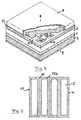
- Contact holes 7 to the buried emitter layers are then etched in order to provide an ohmic contact to each segment in such a way as to limit the resistance to each unit cell and preferably along the perimeter of each segment or directly to each of the individual emitter cells, as shown in Fig. 4 .
- a metal layer 8 is applied on top of the drift layer 6 to make a Schottky contact thereto and in contact with the emitter layer regions.
- the metal used for the Schottky contact may for instance be Ti resulting in a Schottky barrier of about 1.25 eV.
- a metal contact 9 to the opposite side of the diode is also shown in Fig. 4 .
- the contact 9 In the case of an insulating substrate the contact 9 must be arranged to the buffer layer 1 from the top side of the diode.
- Fig. 5 how the etching of square windows through the layer 3 has been carried out for forming laterally extending bars 10 of emitter layer regions crossing each other and forming a bar pattern 11 and a square cell pattern. It is also shown how the metal layer 8 forms an ohmic contact to the emitter layer regions 4 at the perimeter 12 of the segment containing 16 square cells. It is shown as well how the square unit cells are combined into a segment surrounded by a contact to the emitter layer regions 4.
- a diode shown in Figs. 4 and 5 is obvious to a person with ordinary skill in the art, but it will in any way be briefly explained.
- the diode In the forward conducting state of the diode it will due to the lower Schottky barrier (about 1.25 V) than the pn-barrier (about 2.5 V) function as a Schottky diode at lower current densities, so that the on-state losses will be lower than for a pn-diode.
- JBS Junction Barrier Schottky diode
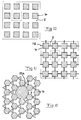
- Fig 6 is a top view of an alternative design of said windows 5, which here have a rectangular shape and are surrounded by emitter layer regions 4 in the form of bars for forming rectangular cells 15a consisting each of a window 5 and part of the surrounding emitter layer region 4 as indicated through the dashed line 16.
- the unit cells are combined into a segment 17, to which contact may be made at any location for making contact to all emitter layer regions included in the segment.
- Fig 7 is a view similar to Fig 6 , in which the windows 5 are squares, as shown in Fig 5 .
- a unit cell is indicated by 15b.
- Fig 8 shows windows 5 in the form of hexagons and how a unit cell 15c is defined.
- Fig 9 shows how islands 4' of emitter layer regions may be formed, in this embodiment with a hexagonal shape while being surrounded by said windows 5', which are here only partially surrounded by emitter layer regions 4'. It is shown how a unit cell 15d is formed by a hexagonal emitter layer region 4' and parts of a window surrounding it. It is also shown how emitter layer regions 4' are in rows electrically connected to each other (18), and an ohmic contact may be obtained to all the cells of such a row by making contact to any cell of the row.
- the embodiment according to Fig 9 is inverted with respect to the embodiment in Fig 8 .
- An advantage of the hexagonal shape is that the distance of a hexagon to adjacent hexagons will be the same around the entire periphery of the hexagon.
- Fig 10 and Fig 11 show in a similar way a structure being inverted with respect to the structure shown in Fig 7 , so that the emitter layer regions are here formed by square islands, in which the contact making thereto is illustrated in Fig 11 .
- Fig 12 shows an alternative structure with an hexagonal pattern having a somewhat larger contact cell 15e, through which contact is made to all the other smaller cells with a hexagonal shape included in the segment shown in Fig 12 .
- step b) It is for instance possible to carry out the etching in step b) further than just to the first drift layer for forming cavities or pockets therein, which may then in the regrowth step c) be filled with material having a lower doping concentration than surrounding first drift layer portions for making the drift layer portions separating the emitter layer regions more easily depleted.
- Low doped as used for the drift layer (first and second drift layers) means a doping concentration being at least one order of magnitude, preferably at least 1.5 order of magnitude, lower than the doping concentration of the second conductivity type layer.
- Windows is to be interpreted as an opening through the emitter layer reaching the drift layer thereunder and at least partially surrounded by emitter layer regions.
Landscapes
- Electrodes Of Semiconductors (AREA)
- Recrystallisation Techniques (AREA)
Applications Claiming Priority (1)
| Application Number | Priority Date | Filing Date | Title |
|---|---|---|---|
| SE0801792 | 2008-08-14 |
Publications (2)
| Publication Number | Publication Date |
|---|---|
| EP2154726A2 true EP2154726A2 (de) | 2010-02-17 |
| EP2154726A3 EP2154726A3 (de) | 2010-05-26 |
Family
ID=41327657
Family Applications (1)
| Application Number | Title | Priority Date | Filing Date |
|---|---|---|---|
| EP09161457A Withdrawn EP2154726A3 (de) | 2008-08-14 | 2009-05-29 | Verfahren zur Herstellung einer JBS Diode |
Country Status (1)
| Country | Link |
|---|---|
| EP (1) | EP2154726A3 (de) |
Cited By (6)
| Publication number | Priority date | Publication date | Assignee | Title |
|---|---|---|---|---|
| CN102376777A (zh) * | 2010-08-24 | 2012-03-14 | 上海芯石微电子有限公司 | 具有低正向压降的结势垒型肖特基 |
| WO2014172164A3 (en) * | 2013-04-19 | 2015-05-14 | Avogy, Inc. | Method of fabricating a merged p-n junction and schottky diode with regrown gallium nitride layer |
| CN108538925A (zh) * | 2018-06-15 | 2018-09-14 | 深圳基本半导体有限公司 | 一种碳化硅结势垒肖特基二极管 |
| CN110676308A (zh) * | 2019-10-12 | 2020-01-10 | 中国电子科技集团公司第十三研究所 | 肖特基二极管的制备方法 |
| CN110931571A (zh) * | 2019-12-18 | 2020-03-27 | 中山大学 | 一种垂直型GaN基凹槽结势垒肖特基二极管及其制作方法 |
| CN111725329A (zh) * | 2019-03-22 | 2020-09-29 | 意法半导体股份有限公司 | 具有减少的电流拥挤效应的半导体mps二极管及其制造方法 |
Citations (2)
| Publication number | Priority date | Publication date | Assignee | Title |
|---|---|---|---|---|
| US6104043A (en) | 1997-01-20 | 2000-08-15 | Abb Research Ltd. | Schottky diode of SiC and a method for production thereof |
| WO2002099869A1 (en) * | 2001-05-25 | 2002-12-12 | Abb Research Limited | A method concerning a junction barrier schottky diode, such a diode and use thereof |
Family Cites Families (4)
| Publication number | Priority date | Publication date | Assignee | Title |
|---|---|---|---|---|
| DE19723176C1 (de) * | 1997-06-03 | 1998-08-27 | Daimler Benz Ag | Leistungshalbleiter-Bauelement und Verfahren zu dessen Herstellung |
| US6462393B2 (en) * | 2001-03-20 | 2002-10-08 | Fabtech, Inc. | Schottky device |
| US20070228505A1 (en) * | 2006-04-04 | 2007-10-04 | Mazzola Michael S | Junction barrier schottky rectifiers having epitaxially grown p+-n junctions and methods of making |
| US7728402B2 (en) * | 2006-08-01 | 2010-06-01 | Cree, Inc. | Semiconductor devices including schottky diodes with controlled breakdown |
-
2009
- 2009-05-29 EP EP09161457A patent/EP2154726A3/de not_active Withdrawn
Patent Citations (2)
| Publication number | Priority date | Publication date | Assignee | Title |
|---|---|---|---|---|
| US6104043A (en) | 1997-01-20 | 2000-08-15 | Abb Research Ltd. | Schottky diode of SiC and a method for production thereof |
| WO2002099869A1 (en) * | 2001-05-25 | 2002-12-12 | Abb Research Limited | A method concerning a junction barrier schottky diode, such a diode and use thereof |
Cited By (8)
| Publication number | Priority date | Publication date | Assignee | Title |
|---|---|---|---|---|
| CN102376777A (zh) * | 2010-08-24 | 2012-03-14 | 上海芯石微电子有限公司 | 具有低正向压降的结势垒型肖特基 |
| WO2014172164A3 (en) * | 2013-04-19 | 2015-05-14 | Avogy, Inc. | Method of fabricating a merged p-n junction and schottky diode with regrown gallium nitride layer |
| CN108538925A (zh) * | 2018-06-15 | 2018-09-14 | 深圳基本半导体有限公司 | 一种碳化硅结势垒肖特基二极管 |
| CN108538925B (zh) * | 2018-06-15 | 2024-05-14 | 深圳基本半导体有限公司 | 一种碳化硅结势垒肖特基二极管 |
| CN111725329A (zh) * | 2019-03-22 | 2020-09-29 | 意法半导体股份有限公司 | 具有减少的电流拥挤效应的半导体mps二极管及其制造方法 |
| CN110676308A (zh) * | 2019-10-12 | 2020-01-10 | 中国电子科技集团公司第十三研究所 | 肖特基二极管的制备方法 |
| CN110676308B (zh) * | 2019-10-12 | 2022-12-20 | 中国电子科技集团公司第十三研究所 | 肖特基二极管的制备方法 |
| CN110931571A (zh) * | 2019-12-18 | 2020-03-27 | 中山大学 | 一种垂直型GaN基凹槽结势垒肖特基二极管及其制作方法 |
Also Published As
| Publication number | Publication date |
|---|---|
| EP2154726A3 (de) | 2010-05-26 |
Similar Documents
| Publication | Publication Date | Title |
|---|---|---|
| US6104043A (en) | Schottky diode of SiC and a method for production thereof | |
| US8232558B2 (en) | Junction barrier Schottky diodes with current surge capability | |
| US6524900B2 (en) | Method concerning a junction barrier Schottky diode, such a diode and use thereof | |
| US8901699B2 (en) | Silicon carbide junction barrier Schottky diodes with suppressed minority carrier injection | |
| US7781786B2 (en) | Semiconductor device having a heterojunction diode and manufacturing method thereof | |
| JP5559530B2 (ja) | 接合障壁ショットキー整流器およびその製造方法 | |
| KR101668215B1 (ko) | 제어가능 온-상태 전압을 가진 전력 반도체 정류기 | |
| JP5172916B2 (ja) | 半導体整流装置 | |
| JP6844163B2 (ja) | 炭化珪素半導体装置 | |
| US8154026B2 (en) | Silicon carbide bipolar semiconductor device | |
| CN119422458A (zh) | 用于沟槽半导体器件的支撑屏蔽结构 |
Legal Events
| Date | Code | Title | Description |
|---|---|---|---|
| PUAI | Public reference made under article 153(3) epc to a published international application that has entered the european phase |
Free format text: ORIGINAL CODE: 0009012 |
|
| AK | Designated contracting states |
Kind code of ref document: A2 Designated state(s): AT BE BG CH CY CZ DE DK EE ES FI FR GB GR HR HU IE IS IT LI LT LU LV MC MK MT NL NO PL PT RO SE SI SK TR |
|
| PUAL | Search report despatched |
Free format text: ORIGINAL CODE: 0009013 |
|
| AK | Designated contracting states |
Kind code of ref document: A3 Designated state(s): AT BE BG CH CY CZ DE DK EE ES FI FR GB GR HR HU IE IS IT LI LT LU LV MC MK MT NL NO PL PT RO SE SI SK TR |
|
| 17P | Request for examination filed |
Effective date: 20101126 |
|
| RAP1 | Party data changed (applicant data changed or rights of an application transferred) |
Owner name: ACREO SWEDISH ICT AB |
|
| 17Q | First examination report despatched |
Effective date: 20130325 |
|
| RAP1 | Party data changed (applicant data changed or rights of an application transferred) |
Owner name: ASCATRON AB |
|
| STAA | Information on the status of an ep patent application or granted ep patent |
Free format text: STATUS: THE APPLICATION IS DEEMED TO BE WITHDRAWN |
|
| 18D | Application deemed to be withdrawn |
Effective date: 20171201 |