EP2154796A1 - Vorrichtung und verfahren zum empfang eines dopsk-signals und verfahren zum erhalten eines dopsk-signals - Google Patents
Vorrichtung und verfahren zum empfang eines dopsk-signals und verfahren zum erhalten eines dopsk-signals Download PDFInfo
- Publication number
- EP2154796A1 EP2154796A1 EP08863384A EP08863384A EP2154796A1 EP 2154796 A1 EP2154796 A1 EP 2154796A1 EP 08863384 A EP08863384 A EP 08863384A EP 08863384 A EP08863384 A EP 08863384A EP 2154796 A1 EP2154796 A1 EP 2154796A1
- Authority
- EP
- European Patent Office
- Prior art keywords
- signal
- dqpsk
- optical
- signals
- dqpsk signal
- Prior art date
- Legal status (The legal status is an assumption and is not a legal conclusion. Google has not performed a legal analysis and makes no representation as to the accuracy of the status listed.)
- Granted
Links
Images



Classifications
-
- H—ELECTRICITY
- H04—ELECTRIC COMMUNICATION TECHNIQUE
- H04B—TRANSMISSION
- H04B10/00—Transmission systems employing electromagnetic waves other than radio-waves, e.g. infrared, visible or ultraviolet light, or employing corpuscular radiation, e.g. quantum communication
- H04B10/50—Transmitters
- H04B10/501—Structural aspects
- H04B10/503—Laser transmitters
- H04B10/505—Laser transmitters using external modulation
-
- H—ELECTRICITY
- H04—ELECTRIC COMMUNICATION TECHNIQUE
- H04B—TRANSMISSION
- H04B10/00—Transmission systems employing electromagnetic waves other than radio-waves, e.g. infrared, visible or ultraviolet light, or employing corpuscular radiation, e.g. quantum communication
- H04B10/50—Transmitters
- H04B10/516—Details of coding or modulation
- H04B10/548—Phase or frequency modulation
- H04B10/556—Digital modulation, e.g. differential phase shift keying [DPSK] or frequency shift keying [FSK]
- H04B10/5561—Digital phase modulation
-
- H—ELECTRICITY
- H04—ELECTRIC COMMUNICATION TECHNIQUE
- H04B—TRANSMISSION
- H04B10/00—Transmission systems employing electromagnetic waves other than radio-waves, e.g. infrared, visible or ultraviolet light, or employing corpuscular radiation, e.g. quantum communication
- H04B10/60—Receivers
- H04B10/66—Non-coherent receivers, e.g. using direct detection
- H04B10/67—Optical arrangements in the receiver
- H04B10/676—Optical arrangements in the receiver for all-optical demodulation of the input optical signal
- H04B10/677—Optical arrangements in the receiver for all-optical demodulation of the input optical signal for differentially modulated signal, e.g. DPSK signals
Definitions
- the present invention relates to the field of mobile communication technology, and more particularly to a device and a method for receiving a differential quadrature phase shift keying (DQPSK) signal and a method for obtaining a DQPSK signal.
- DQPSK differential quadrature phase shift keying
- the signal transmission performance is affected by various transmission impairments of transmission links such as chromatic dispersion, non-linear effects, and polarization mode dispersion (PMD).
- PMD polarization mode dispersion
- novel modulation formats capable of effectively reducing the influence caused by impairments of the transmission links have come into being. It is generally recognized that, a DQPSK as a vector modulation format reported in literature during OFC2002 is the most promising modulation format for transmission systems of higher than 40 Gb/s.
- the DQPSK has a very small spectrum width and realizes a channel spacing of 12.5-25 GHz in DWDM systems of 10 Gbit/s; as compared with known modulation formats for optical modulation systems such as Non Return to Zero (NRZ) and binary differential phase shift keying (DPSK), at the same symbol rate, the DQPSK maintains the chromatic dispersion tolerance unchanged, but the system capacity thereof is twice of that of the modulation formats such as NRZ and DPSK; since the DQPSK can realize constant-envelope transmission or near constant-envelope transmission, various non-linear effects of the optical fibers, such as cross phase modulation (XPM) and self phase modulation (SPM), can be inhibited; and the DQPSK has a large symbol delay, and can improve the chromatic dispersion tolerance and PMD tolerance as well as spectral efficiency.
- NRZ Non Return to Zero
- DPSK binary differential phase shift keying
- a DQPSK signal transmitting end uses a pre-coding module to pre-code two input data signals u and v, so as to generate two driving electric signals I and Q.
- the driving electric signals I and Q respectively drive an upper branch and a lower branch of a dual-parallel MZ modulator, such that Mach-Zehnder modulators (MZMs) modulate a real part and an imaginary part of an input optical carrier to generate a real-part signal and an imaginary-part signal.
- MZMs Mach-Zehnder modulators
- the imaginary-part signal is combined with the real-part signal to generate an optical DQPSK signal.
- a DQPSK signal receiving end receives the DQPSK signal, uses a splitter to split the DQPSK signal into an upper optical signal and a lower optical signal, uses two Mach-Zehnder interferometers (MZIs) to respectively demodulate the upper optical signal and the lower optical signal of the DQPSK, and then uses two balanced receivers to recover signals u and v from the optical signals, thereby completing the receiving and demodulation of the signal.
- MZIs Mach-Zehnder interferometers
- the demodulation manner is rather complex, and has a high cost.
- the MZIs have poor stability and are polarization dependent, the performance of the optical transmission system is greatly affected.
- the present invention is directed to a device and a method for receiving a DQPSK signal, which are applicable to improve performance of an optical transmission system while ensuring simple demodulation of the DQPSK signal.
- the present invention is also directed to a method for obtaining a DQPSK signal, so as to enable the DQPSK signal obtained through the method to be easily received and processed by a DQPSK signal receiving end.
- the present invention provides a device for receiving a DQPSK signal, which includes: a splitter, adapted to split the DQPSK signal to obtain two optical signals; two optical bandpass filters, connected to the splitter, and adapted to optically bandpass filter the two optical signals respectively, in which the two optical bandpass filters respectively have a positive frequency offset and a negative frequency offset from a central frequency of the DQPSK signal received by the splitter; and two photoelectric detectors, correspondingly connected to the two optical bandpass filters, and adapted to photoelectrically convert the filtered optical signals to obtain data signals.
- the DQPSK signal is filtered and demodulated by the optical bandpass filters, and then photoelectrically converted by the photoelectric detectors to recover the data signals, such that the problems of poor stability and polarization dependence caused by the MZI are avoided, thereby greatly improving the performance of the optical transmission system.
- the present invention further provides a method for receiving a DQPSK signal, which includes the following steps.
- the DQPSK signal is split to obtain two optical signals.
- the two optical signals are respectively optically bandpass filtered by two optical bandpass filters that respectively have a positive frequency offset and a negative frequency offset from a central frequency of the DQPSK signal.
- the filtered optical signals are respectively photoelectrically converted to obtain data signals.
- the demodulation module provided by the embodiments of the present invention is quite simple.
- the demodulation module uses the adjustable filters to demodulate the DQPSK signal, which thus has high stability and polarization independence features.
- the DQPSK signal at a higher rate can be demodulated by simply increasing the bandwidth and offset of the optical bandpass filters, and the increased bandwidth further enables the optical bandpass filters to be easily manufactured. Therefore, the higher the signal transmission rate is, the more easily the device is manufactured.
- the present invention further provides a method for obtaining a DQPSK signal, which includes the following steps.
- Q k u ⁇ ⁇ v ⁇ ⁇ Q k - 1 + u ⁇ v ⁇ ⁇ I ⁇ k - 1 + u ⁇ ⁇ v ⁇ I k - 1 + uv ⁇ Q ⁇ k - 1 or
- I k u ⁇ ⁇ I k - 1 ⁇ Q ⁇ k - 1 + v ⁇ I ⁇ k - 1 ⁇ Q ⁇ k - 1 + u ⁇ I ⁇ k - 1 ⁇ Q k - 1 + v ⁇ I k - 1 ⁇ Q k - 1 +
- An input optical carrier is modulated by using the two driving signals respectively, so as to obtain a real-part signal and an imaginary-part signal.
- the real-part signal and the imaginary-part signal are combined to generate the DQPSK signal.
- the pre-coding method is adopted to enable an obtained corresponding relation between a phase shift value of the DQPSK signal and bit information of the data signals to be consistent with a corresponding relation between a phase shift value of the DQPSK signal and the optical signals obtained through demodulation at the DQPSK signal receiving end, such that the data signals are directly obtained after the DQPSK signal receiving end photoelectrically converts the optical signals obtained by filtering and demodulation, thereby further simplifying the construction of the DQPSK signal receiving end.
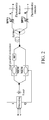
- FIG. 2 is a schematic structural view of a first embodiment of a device for receiving a DQPSK signal according to the present invention.
- a DQPSK signal transmitting end still adopts an existing device, except for disposing a 90° phase shifter after an MZM that generates a real-part signal.
- a pre-coding module pre-codes data signals u and v by using coding rules listed in Table 1 and generates two driving electric signals I and Q.
- the driving electric signals I and Q respectively drive an upper branch MZM and a lower branch MZM of a dual-parallel modulator to modulate a real part and an imaginary part of an input optical carrier emitted by a laser, so as to generate a real-part signal and an imaginary-part signal.
- the real-part signal and the imaginary-part signal are combined to generate a DQPSK signal, which is transmitted to a DQPSK signal receiving device through optical fibers.
- the DQPSK signal receiving device includes a splitter, and optical bandpass filters and photoelectric detectors sequentially connected to the splitter.
- an optical bandpass filter whose central wavelength has a negative wavelength offset (corresponding to a positive frequency offset) from a central wavelength of the DQPSK signal is referred to as BPF1
- an optical bandpass filter whose central wavelength has a positive wavelength offset (corresponding to a negative frequency offset) from the central wavelength of the DQPSK signal is referred to as BPF2.
- the absolute values of the frequency offsets of the bandpass filters are preferably 0.6B-2B, so that the absolute values of the wavelength shifts thereof are derived as 0.6 ⁇ B ⁇ ⁇ c 2 c - 2 ⁇ B ⁇ ⁇ c 2 c , in which c is the velocity of light and ⁇ c is the central wavelength.
- the splitter splits the DQPSK signal into two optical signals, the BPF1 demodulates one optical signal to obtain a demodulated optical signal A, the BPF2 demodulates the other optical signal to obtain a demodulated optical signal B, and then A and B are respectively photoelectrically converted by a photoelectric detector, so as to respectively recover the data signals u and v.
- the 90° phase shifter at the DQPSK signal receiving end may also be disposed after an MZM that generates an imaginary-part signal.
- the data signal recovered by the BPF1 and the photoelectric detector is v
- the data signal recovered by the BPF2 and the photoelectric detector is u.
- the DQPSK signal receiving device in this embodiment uses the optical bandpass filters for demodulation, the problems about complex demodulation, poor transmission performance, and high cost brought by the MZI are solved.
- the demodulation operation in the DQPSK signal receiving device is simplified, and the transmission performance is improved.
- Initial values of I and Q may be 00, 01, 10, or 11.
- initial values of I and Q are 11, as for data signals u and v given as follows, corresponding values of the driving electric signals I and Q are listed as follows. u 0001010001011001100 v 0001110001101001001 I11110100001110001001 Q11110011110101110000
- the driving electric signals I and Q respectively drive the upper branch and the lower branch of the dual-parallel modulator, and the dual-parallel modulator outputs the DQPSK signal.
- the modulation principle is analyzed as follows.
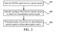
- Step 101 the splitter splits the DQPSK signal into two optical signals.
- the BPF1 and the BPF2 optically bandpass filter each optical signal respectively, that is, performing demodulation on each optical signal.
- Central wavelengths of the two optical bandpass filters, the BPF1 and the BPF2 respectively have a negative wavelength offset and a positive wavelength offset from a central wavelength of the DQPSK signal.
- the wavelength shifts should be selected in such a way that the optical signals demodulated through the optical bandpass filters have an optimal performance, and the absolute values of the frequency offsets of the BPF1 and the BPF2 are most preferably about 1 time of the transmission rate of the DQPSK signal.
- the upper and lower demodulated optical signals A and B have the optimal performance. That is, an optimal performance may be achieved when the offset is preferably approximately equal to the transmission rate (bandwidth).
- FIGs. 4A and 4B respectively show an output waveform of the BPF1 and an output waveform of the BPF2 obtained by emulation. It can be seen that, waveforms of A and B are one-to-one corresponding to u and v provided above in this embodiment.
- the DQPSK signal at a higher rate can be demodulated by simply increasing the bandwidth and offset of the optical bandpass filters. In addition, the increased bandwidth enables the optical bandpass filters to be easily manufactured.
- the bandpass filter BPF1 has a certain frequency offset, such that an edge of a filter amplitude spectrum passes through the major lobe of the DQPSK signal. If the edge of the filter amplitude spectrum is approximated as a sloped straight line Kw (K is a positive constant), the major lobe of the DQPSK frequency spectrum is H DQPSK ( w ) Kw after passing through the edge of the filter.
- the frequency domain expression turns to be KE DQPSK t ⁇ d f t d t after an inverse Fourier transform.
- the demodulation principle of using the bandpass filters is to convert phase shift information of the DQPSK into amplitude information, thereby achieving the demodulation and recovering the original bit information.
- the sinusoidal signal includes a rising edge from 0 to 1 and a falling edge from 1 to 0.
- d f t d t is a positive value
- the BPF1 has a pulse output
- d f t d t is a negative value
- the BPF1 has no pulse output.
- D ⁇ f DQPSK - p 2
- d f t d t is a negative value
- the optical signals A and B obtained through demodulation by the BPF1 and the BPF2 are corresponding to the bit information of the original data signals.
- Step 103 the optical signals A and B are respectively photoelectrically converted by the photoelectric detectors to obtain data signals u and v.
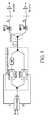
- FIG. 5 is a schematic structural view of a second embodiment of the device for receiving a DQPSK signal according to the present invention.
- an inverter may be further added after photoelectric detectors at a DQPSK signal receiving device. After upper and lower demodulated optical signals pass through the upper and lower photoelectric detectors, inverse signals u and v are respectively generated. Then, the inverter recovers data signals u and v from the inverse signals u and v .
- I k uv ⁇ I k - 1 + u ⁇ v ⁇ ⁇ Q ⁇ k - 1 + u ⁇ ⁇ v ⁇ ⁇ I ⁇ k - 1 + u ⁇ ⁇ v ⁇ Q k - 1
- Q k uv ⁇ Q k - 1 + u ⁇ ⁇ v ⁇ I ⁇ k - 1 + u ⁇ v ⁇ I k - 1 + u ⁇ v ⁇ ⁇ Q ⁇ k - 1 or
- I k u ⁇ I k - 1 ⁇ Q ⁇ k - 1 + v ⁇ ⁇ I ⁇ k - 1 ⁇ Q ⁇ k - 1 + u ⁇ ⁇ I ⁇ k - 1 ⁇ Q k - 1 + v ⁇ I k - 1 ⁇ Q k - 1 + v ⁇ I k - 1 ⁇ Q k - 1 +
- the DQPSK elements corresponding to the data signals u and v and the phase shift values of the adjacent DQPSK elements are shown as follows.
- the receiving device After the receiving device receives the DQPSK signal, the following steps are performed.
- Step 201 the splitter splits the DQPSK signal into two optical signals.
- Step 202 the BPF1 and the BPF2 respectively demodulate the optical signals, and the table of the corresponding relation between the obtained optical signals A and B and the phase shift value of adjacent DQPSK elements remains unchanged, which is still Table 2.
- the corresponding relation between the data signals u and v and the phase shift value of adjacent DQPSK elements has changed, as shown in Table 4.
- the optical signal A obtained by demodulation is an inverse of the bit information of the data signal u
- the optical signal B obtained by demodulation is an inverse of the bit information of the data signal v.
- Step 203 after A and B pass through the photoelectric detectors, signals inversed to the signals u and v, that is, u and v , are obtained.
- the original data signals u and v can be obtained through a further inversion.
- Step 204 u and v respectively pass through an inverter, such that the original input data signals are obtained.
- the device since the DQPSK signal is demodulated by using the optical bandpass filters, the device is quite simple, and has high stability, and polarization independent features. Moreover, the higher the signal transmission rate is, the more easily the device is manufactured. Thus, the performance of the optical transmission system is greatly improved, and the demodulation cost is greatly reduced.
Landscapes
- Physics & Mathematics (AREA)
- Electromagnetism (AREA)
- Engineering & Computer Science (AREA)
- Computer Networks & Wireless Communication (AREA)
- Signal Processing (AREA)
- Optics & Photonics (AREA)
- Optical Communication System (AREA)
- Digital Transmission Methods That Use Modulated Carrier Waves (AREA)
Applications Claiming Priority (2)
| Application Number | Priority Date | Filing Date | Title |
|---|---|---|---|
| CN200710179571.6A CN101459638B (zh) | 2007-12-14 | 2007-12-14 | 差分正交相移键控dqpsk信号的接收装置及方法 |
| PCT/CN2008/073206 WO2009076830A1 (zh) | 2007-12-14 | 2008-11-26 | 差分正交相移键控信号的接收装置及方法、获取方法 |
Publications (3)
| Publication Number | Publication Date |
|---|---|
| EP2154796A1 true EP2154796A1 (de) | 2010-02-17 |
| EP2154796A4 EP2154796A4 (de) | 2011-07-13 |
| EP2154796B1 EP2154796B1 (de) | 2015-08-19 |
Family
ID=40770274
Family Applications (1)
| Application Number | Title | Priority Date | Filing Date |
|---|---|---|---|
| EP08863384.7A Not-in-force EP2154796B1 (de) | 2007-12-14 | 2008-11-26 | Vorrichtung und verfahren zum empfang eines dopsk-signals und verfahren zum erhalten eines dopsk-signals |
Country Status (4)
| Country | Link |
|---|---|
| US (1) | US8270848B2 (de) |
| EP (1) | EP2154796B1 (de) |
| CN (1) | CN101459638B (de) |
| WO (1) | WO2009076830A1 (de) |
Cited By (1)
| Publication number | Priority date | Publication date | Assignee | Title |
|---|---|---|---|---|
| EP2326033A4 (de) * | 2008-06-30 | 2011-12-28 | Huawei Tech Co Ltd | Differenz-quadraturphasenumtastsystem, verfahren und geräte |
Families Citing this family (13)
| Publication number | Priority date | Publication date | Assignee | Title |
|---|---|---|---|---|
| KR101382619B1 (ko) * | 2009-07-24 | 2014-04-07 | 한국전자통신연구원 | 광 송신 장치 및 방법과 광 수신 장치 및 방법 |
| CN102109732B (zh) * | 2009-12-23 | 2013-10-30 | 菲尼萨公司 | 差分正交相移键控解调器 |
| CN101895495B (zh) * | 2010-07-15 | 2012-12-12 | 北京邮电大学 | 正交双偏振差分四相相移键控发射与接收的方法及其系统 |
| CN102170307B (zh) * | 2010-12-14 | 2014-01-08 | 华为技术有限公司 | 动态频偏矫正的方法及相干光时域反射仪系统 |
| CN102354076B (zh) * | 2011-06-29 | 2013-08-14 | 华中科技大学 | 一种光连续相位调制和解调装置 |
| EP2761835A4 (de) * | 2011-09-30 | 2015-05-06 | Intel Corp | Verfahren und anordnungen für kommunikationen mit frequenzverschiebung |
| CN102833205B (zh) * | 2012-09-06 | 2015-04-29 | 昆山胜泽光电科技有限公司 | 非等间距dqpsk耦合干涉信号解调方法 |
| US10291329B2 (en) * | 2013-12-20 | 2019-05-14 | Infineon Technologies Ag | Exchanging information between time-of-flight ranging devices |
| CN104330905B (zh) * | 2014-11-12 | 2019-11-08 | 天津工业大学 | 基于二维光栅耦合的硅基qpsk光调制器 |
| US10551640B2 (en) * | 2016-11-21 | 2020-02-04 | Futurewei Technologies, Inc. | Wavelength division multiplexed polarization independent reflective modulators |
| US10222676B2 (en) | 2017-01-27 | 2019-03-05 | Futurewei Technologies, Inc. | Polarization insensitive integrated optical modulator |
| US10330959B2 (en) | 2017-05-22 | 2019-06-25 | Futurewei Technologies, Inc. | Polarization insensitive micro ring modulator |
| US10243684B2 (en) | 2017-05-23 | 2019-03-26 | Futurewei Technologies, Inc. | Wavelength-division multiplexed polarization-insensitive transmissive modulator |
Family Cites Families (16)
| Publication number | Priority date | Publication date | Assignee | Title |
|---|---|---|---|---|
| US5953140A (en) * | 1997-09-30 | 1999-09-14 | Mci Communications Corporation | Electrical domain improvement of optically filtered signals |
| US6980747B1 (en) * | 2000-11-28 | 2005-12-27 | Harris Corporation | Optically amplified receiver |
| GB2383705B (en) * | 2001-11-30 | 2005-03-30 | Marconi Optical Components Ltd | Optical coding system |
| US7349636B2 (en) * | 2003-12-11 | 2008-03-25 | Mario Zitelli | Optical phase and intensity modulation with improved transmitters |
| JP4170298B2 (ja) | 2005-01-31 | 2008-10-22 | 富士通株式会社 | 差分4位相偏移変調方式に対応した光受信器および光受信方法 |
| US7398022B2 (en) * | 2005-07-08 | 2008-07-08 | Mario Zitelli | Optical return-to-zero phase-shift keying with improved transmitters |
| ATE390768T1 (de) * | 2005-11-25 | 2008-04-15 | Alcatel Lucent | Faseroptisches übertragungssystem, sender und empfänger für dqpsk modulierte signale und zugehöriges stabilisierungsverfahren |
| JP4768421B2 (ja) * | 2005-12-06 | 2011-09-07 | 富士通株式会社 | Dqpsk光受信器 |
| JP4563944B2 (ja) * | 2006-01-31 | 2010-10-20 | 富士通株式会社 | 光送信器 |
| JP2007274235A (ja) * | 2006-03-30 | 2007-10-18 | Fujitsu Ltd | 光dqpsk受信器 |
| US8503889B2 (en) * | 2007-03-23 | 2013-08-06 | Massachusetts Institute Of Technology | Filter-based DPSK receiver |
| US8300157B2 (en) * | 2007-11-06 | 2012-10-30 | Himax Technologies Limited | Method for estimating frequency offsets and frequency offset estimation circuit thereof |
| US8582705B2 (en) * | 2007-12-10 | 2013-11-12 | Ciena Corporation | Serializer-deserializer circuit with multi-format and multi-data rate capability |
| US8032036B2 (en) * | 2007-12-10 | 2011-10-04 | Verizon Patent And Licensing Inc. | DQPSK/DPSK optical receiver with tunable optical fibers |
| CN101621336B (zh) * | 2008-06-30 | 2012-12-12 | 华为技术有限公司 | 一种差分正交相移键控系统、方法及设备 |
| JP5245736B2 (ja) * | 2008-11-10 | 2013-07-24 | 富士通株式会社 | プリコーダ回路 |
-
2007
- 2007-12-14 CN CN200710179571.6A patent/CN101459638B/zh not_active Expired - Fee Related
-
2008
- 2008-11-26 WO PCT/CN2008/073206 patent/WO2009076830A1/zh not_active Ceased
- 2008-11-26 EP EP08863384.7A patent/EP2154796B1/de not_active Not-in-force
-
2010
- 2010-06-01 US US12/791,536 patent/US8270848B2/en not_active Expired - Fee Related
Cited By (1)
| Publication number | Priority date | Publication date | Assignee | Title |
|---|---|---|---|---|
| EP2326033A4 (de) * | 2008-06-30 | 2011-12-28 | Huawei Tech Co Ltd | Differenz-quadraturphasenumtastsystem, verfahren und geräte |
Also Published As
| Publication number | Publication date |
|---|---|
| CN101459638B (zh) | 2012-03-21 |
| US8270848B2 (en) | 2012-09-18 |
| WO2009076830A1 (zh) | 2009-06-25 |
| CN101459638A (zh) | 2009-06-17 |
| EP2154796A4 (de) | 2011-07-13 |
| US20100254719A1 (en) | 2010-10-07 |
| EP2154796B1 (de) | 2015-08-19 |
Similar Documents
| Publication | Publication Date | Title |
|---|---|---|
| EP2154796A1 (de) | Vorrichtung und verfahren zum empfang eines dopsk-signals und verfahren zum erhalten eines dopsk-signals | |
| CN100481824C (zh) | 光通信的改进 | |
| US8655196B2 (en) | Phase control circuit and method for optical receivers | |
| US10895797B2 (en) | Line coding for optical transmission | |
| US7277647B2 (en) | System and method of optical transmission | |
| CN101432998A (zh) | 部分dpsk(pdpsk)传输系统 | |
| US7398022B2 (en) | Optical return-to-zero phase-shift keying with improved transmitters | |
| EP1612972B1 (de) | Verfahren und Vorrichtung zur Erzeugung von CRZ-DPSK optischen signalen | |
| US8208816B2 (en) | Method and apparatus for dispersion mitigation in optical links | |
| EP1851884A1 (de) | Optisches msk-datenformat | |
| Lu et al. | 80-Gb/s optical MSK generation using a monolithically integrated quad-mach-zehnder IQ modulator | |
| Tokle et al. | Wavelength conversion of 80 Gbit/s optical DQPSK using FWM in a highly non-linear fibre | |
| Adalid | Modulation format conversion in future optical networks | |
| Lyubomirsky | Advanced modulation formats for ultra-dense wavelength division multiplexing | |
| Han et al. | Differential polarization-phase-shift keying without using polarization control | |
| Fujita et al. | 80 Gb/s optical quadrature phase shift keying modulation using an integrated LiNbO3 modulator | |
| Chi et al. | FSK Modulation Scheme for High-Speed Optical Transmission | |
| Ibrahim | Study of multilevel modulation formats for high speed digital optical communication systems | |
| Lu et al. | A spectrum-efficient 80-Gbit/s DPSK transmitter using phase interleaving technology without optical-time or polarization-division multiplexing | |
| Haris et al. | Impact of free spectral range optimization on RZ/NRZ DQPSK modulation format with strong optical filtering for Ultra-High data rate systems | |
| Yu et al. | Simple and flexible optical NRZ-DQPSK demodulation and detection scheme | |
| Kumar et al. | High-Speed Phase-Correlated Signal Generation by Phase Reconstruction of OTDM Signals through Differential Cross-Phase Modulation in an SOA-MZI | |
| Mo | Advanced modulation formats for high capacity optical communication systems | |
| da Costa | OPTICAL FIBRE TELECOMMUNICATION SYSTEMS |
Legal Events
| Date | Code | Title | Description |
|---|---|---|---|
| PUAI | Public reference made under article 153(3) epc to a published international application that has entered the european phase |
Free format text: ORIGINAL CODE: 0009012 |
|
| 17P | Request for examination filed |
Effective date: 20091127 |
|
| AK | Designated contracting states |
Kind code of ref document: A1 Designated state(s): AT BE BG CH CY CZ DE DK EE ES FI FR GB GR HR HU IE IS IT LI LT LU LV MC MT NL NO PL PT RO SE SI SK TR |
|
| AX | Request for extension of the european patent |
Extension state: AL BA MK RS |
|
| DAX | Request for extension of the european patent (deleted) | ||
| REG | Reference to a national code |
Ref country code: DE Ref legal event code: R079 Ref document number: 602008039711 Country of ref document: DE Free format text: PREVIOUS MAIN CLASS: H04B0010020000 Ipc: H04B0010155000 Ref country code: DE Ref legal event code: R079 Free format text: PREVIOUS MAIN CLASS: H04B0010020000 Ipc: H04B0010155000 |
|
| A4 | Supplementary search report drawn up and despatched |
Effective date: 20110615 |
|
| RIC1 | Information provided on ipc code assigned before grant |
Ipc: H04B 10/155 20060101AFI20110608BHEP |
|
| 17Q | First examination report despatched |
Effective date: 20130822 |
|
| REG | Reference to a national code |
Ref country code: DE Ref legal event code: R079 Ref document number: 602008039711 Country of ref document: DE Free format text: PREVIOUS MAIN CLASS: H04B0010155000 Ipc: H04B0010500000 |
|
| RIC1 | Information provided on ipc code assigned before grant |
Ipc: H04B 10/50 20130101AFI20141125BHEP Ipc: H04B 10/556 20130101ALI20141125BHEP Ipc: H04B 10/67 20130101ALI20141125BHEP |
|
| GRAP | Despatch of communication of intention to grant a patent |
Free format text: ORIGINAL CODE: EPIDOSNIGR1 |
|
| INTG | Intention to grant announced |
Effective date: 20150227 |
|
| GRAS | Grant fee paid |
Free format text: ORIGINAL CODE: EPIDOSNIGR3 |
|
| GRAA | (expected) grant |
Free format text: ORIGINAL CODE: 0009210 |
|
| AK | Designated contracting states |
Kind code of ref document: B1 Designated state(s): AT BE BG CH CY CZ DE DK EE ES FI FR GB GR HR HU IE IS IT LI LT LU LV MC MT NL NO PL PT RO SE SI SK TR |
|
| REG | Reference to a national code |
Ref country code: GB Ref legal event code: FG4D |
|
| REG | Reference to a national code |
Ref country code: CH Ref legal event code: EP |
|
| REG | Reference to a national code |
Ref country code: IE Ref legal event code: FG4D |
|
| REG | Reference to a national code |
Ref country code: AT Ref legal event code: REF Ref document number: 744439 Country of ref document: AT Kind code of ref document: T Effective date: 20150915 |
|
| REG | Reference to a national code |
Ref country code: DE Ref legal event code: R096 Ref document number: 602008039711 Country of ref document: DE |
|
| REG | Reference to a national code |
Ref country code: FR Ref legal event code: PLFP Year of fee payment: 8 |
|
| REG | Reference to a national code |
Ref country code: AT Ref legal event code: MK05 Ref document number: 744439 Country of ref document: AT Kind code of ref document: T Effective date: 20150819 |
|
| REG | Reference to a national code |
Ref country code: NL Ref legal event code: FP |
|
| REG | Reference to a national code |
Ref country code: LT Ref legal event code: MG4D |
|
| PG25 | Lapsed in a contracting state [announced via postgrant information from national office to epo] |
Ref country code: NO Free format text: LAPSE BECAUSE OF FAILURE TO SUBMIT A TRANSLATION OF THE DESCRIPTION OR TO PAY THE FEE WITHIN THE PRESCRIBED TIME-LIMIT Effective date: 20151119 Ref country code: LT Free format text: LAPSE BECAUSE OF FAILURE TO SUBMIT A TRANSLATION OF THE DESCRIPTION OR TO PAY THE FEE WITHIN THE PRESCRIBED TIME-LIMIT Effective date: 20150819 Ref country code: LV Free format text: LAPSE BECAUSE OF FAILURE TO SUBMIT A TRANSLATION OF THE DESCRIPTION OR TO PAY THE FEE WITHIN THE PRESCRIBED TIME-LIMIT Effective date: 20150819 Ref country code: FI Free format text: LAPSE BECAUSE OF FAILURE TO SUBMIT A TRANSLATION OF THE DESCRIPTION OR TO PAY THE FEE WITHIN THE PRESCRIBED TIME-LIMIT Effective date: 20150819 Ref country code: GR Free format text: LAPSE BECAUSE OF FAILURE TO SUBMIT A TRANSLATION OF THE DESCRIPTION OR TO PAY THE FEE WITHIN THE PRESCRIBED TIME-LIMIT Effective date: 20151120 |
|
| PG25 | Lapsed in a contracting state [announced via postgrant information from national office to epo] |
Ref country code: PT Free format text: LAPSE BECAUSE OF FAILURE TO SUBMIT A TRANSLATION OF THE DESCRIPTION OR TO PAY THE FEE WITHIN THE PRESCRIBED TIME-LIMIT Effective date: 20151221 Ref country code: AT Free format text: LAPSE BECAUSE OF FAILURE TO SUBMIT A TRANSLATION OF THE DESCRIPTION OR TO PAY THE FEE WITHIN THE PRESCRIBED TIME-LIMIT Effective date: 20150819 Ref country code: PL Free format text: LAPSE BECAUSE OF FAILURE TO SUBMIT A TRANSLATION OF THE DESCRIPTION OR TO PAY THE FEE WITHIN THE PRESCRIBED TIME-LIMIT Effective date: 20150819 Ref country code: IS Free format text: LAPSE BECAUSE OF FAILURE TO SUBMIT A TRANSLATION OF THE DESCRIPTION OR TO PAY THE FEE WITHIN THE PRESCRIBED TIME-LIMIT Effective date: 20151219 Ref country code: ES Free format text: LAPSE BECAUSE OF FAILURE TO SUBMIT A TRANSLATION OF THE DESCRIPTION OR TO PAY THE FEE WITHIN THE PRESCRIBED TIME-LIMIT Effective date: 20150819 Ref country code: SE Free format text: LAPSE BECAUSE OF FAILURE TO SUBMIT A TRANSLATION OF THE DESCRIPTION OR TO PAY THE FEE WITHIN THE PRESCRIBED TIME-LIMIT Effective date: 20150819 |
|
| PG25 | Lapsed in a contracting state [announced via postgrant information from national office to epo] |
Ref country code: DK Free format text: LAPSE BECAUSE OF FAILURE TO SUBMIT A TRANSLATION OF THE DESCRIPTION OR TO PAY THE FEE WITHIN THE PRESCRIBED TIME-LIMIT Effective date: 20150819 Ref country code: SK Free format text: LAPSE BECAUSE OF FAILURE TO SUBMIT A TRANSLATION OF THE DESCRIPTION OR TO PAY THE FEE WITHIN THE PRESCRIBED TIME-LIMIT Effective date: 20150819 Ref country code: EE Free format text: LAPSE BECAUSE OF FAILURE TO SUBMIT A TRANSLATION OF THE DESCRIPTION OR TO PAY THE FEE WITHIN THE PRESCRIBED TIME-LIMIT Effective date: 20150819 Ref country code: CZ Free format text: LAPSE BECAUSE OF FAILURE TO SUBMIT A TRANSLATION OF THE DESCRIPTION OR TO PAY THE FEE WITHIN THE PRESCRIBED TIME-LIMIT Effective date: 20150819 |
|
| REG | Reference to a national code |
Ref country code: DE Ref legal event code: R097 Ref document number: 602008039711 Country of ref document: DE |
|
| PG25 | Lapsed in a contracting state [announced via postgrant information from national office to epo] |
Ref country code: RO Free format text: LAPSE BECAUSE OF FAILURE TO SUBMIT A TRANSLATION OF THE DESCRIPTION OR TO PAY THE FEE WITHIN THE PRESCRIBED TIME-LIMIT Effective date: 20150819 |
|
| PLBE | No opposition filed within time limit |
Free format text: ORIGINAL CODE: 0009261 |
|
| STAA | Information on the status of an ep patent application or granted ep patent |
Free format text: STATUS: NO OPPOSITION FILED WITHIN TIME LIMIT |
|
| PG25 | Lapsed in a contracting state [announced via postgrant information from national office to epo] |
Ref country code: LU Free format text: LAPSE BECAUSE OF FAILURE TO SUBMIT A TRANSLATION OF THE DESCRIPTION OR TO PAY THE FEE WITHIN THE PRESCRIBED TIME-LIMIT Effective date: 20151126 Ref country code: MC Free format text: LAPSE BECAUSE OF FAILURE TO SUBMIT A TRANSLATION OF THE DESCRIPTION OR TO PAY THE FEE WITHIN THE PRESCRIBED TIME-LIMIT Effective date: 20150819 |
|
| REG | Reference to a national code |
Ref country code: CH Ref legal event code: PL |
|
| 26N | No opposition filed |
Effective date: 20160520 |
|
| PG25 | Lapsed in a contracting state [announced via postgrant information from national office to epo] |
Ref country code: CH Free format text: LAPSE BECAUSE OF NON-PAYMENT OF DUE FEES Effective date: 20151130 Ref country code: LI Free format text: LAPSE BECAUSE OF NON-PAYMENT OF DUE FEES Effective date: 20151130 |
|
| REG | Reference to a national code |
Ref country code: IE Ref legal event code: MM4A |
|
| PG25 | Lapsed in a contracting state [announced via postgrant information from national office to epo] |
Ref country code: SI Free format text: LAPSE BECAUSE OF FAILURE TO SUBMIT A TRANSLATION OF THE DESCRIPTION OR TO PAY THE FEE WITHIN THE PRESCRIBED TIME-LIMIT Effective date: 20150819 |
|
| REG | Reference to a national code |
Ref country code: FR Ref legal event code: PLFP Year of fee payment: 9 |
|
| PG25 | Lapsed in a contracting state [announced via postgrant information from national office to epo] |
Ref country code: IE Free format text: LAPSE BECAUSE OF NON-PAYMENT OF DUE FEES Effective date: 20151126 |
|
| PG25 | Lapsed in a contracting state [announced via postgrant information from national office to epo] |
Ref country code: BE Free format text: LAPSE BECAUSE OF FAILURE TO SUBMIT A TRANSLATION OF THE DESCRIPTION OR TO PAY THE FEE WITHIN THE PRESCRIBED TIME-LIMIT Effective date: 20150819 |
|
| PG25 | Lapsed in a contracting state [announced via postgrant information from national office to epo] |
Ref country code: HU Free format text: LAPSE BECAUSE OF FAILURE TO SUBMIT A TRANSLATION OF THE DESCRIPTION OR TO PAY THE FEE WITHIN THE PRESCRIBED TIME-LIMIT; INVALID AB INITIO Effective date: 20081126 Ref country code: BG Free format text: LAPSE BECAUSE OF FAILURE TO SUBMIT A TRANSLATION OF THE DESCRIPTION OR TO PAY THE FEE WITHIN THE PRESCRIBED TIME-LIMIT Effective date: 20150819 |
|
| PG25 | Lapsed in a contracting state [announced via postgrant information from national office to epo] |
Ref country code: CY Free format text: LAPSE BECAUSE OF FAILURE TO SUBMIT A TRANSLATION OF THE DESCRIPTION OR TO PAY THE FEE WITHIN THE PRESCRIBED TIME-LIMIT Effective date: 20150819 |
|
| PG25 | Lapsed in a contracting state [announced via postgrant information from national office to epo] |
Ref country code: HR Free format text: LAPSE BECAUSE OF FAILURE TO SUBMIT A TRANSLATION OF THE DESCRIPTION OR TO PAY THE FEE WITHIN THE PRESCRIBED TIME-LIMIT Effective date: 20150819 |
|
| PG25 | Lapsed in a contracting state [announced via postgrant information from national office to epo] |
Ref country code: MT Free format text: LAPSE BECAUSE OF FAILURE TO SUBMIT A TRANSLATION OF THE DESCRIPTION OR TO PAY THE FEE WITHIN THE PRESCRIBED TIME-LIMIT Effective date: 20150819 Ref country code: TR Free format text: LAPSE BECAUSE OF FAILURE TO SUBMIT A TRANSLATION OF THE DESCRIPTION OR TO PAY THE FEE WITHIN THE PRESCRIBED TIME-LIMIT Effective date: 20150819 |
|
| REG | Reference to a national code |
Ref country code: FR Ref legal event code: PLFP Year of fee payment: 10 |
|
| REG | Reference to a national code |
Ref country code: FR Ref legal event code: PLFP Year of fee payment: 11 |
|
| PGFP | Annual fee paid to national office [announced via postgrant information from national office to epo] |
Ref country code: NL Payment date: 20201113 Year of fee payment: 13 |
|
| PGFP | Annual fee paid to national office [announced via postgrant information from national office to epo] |
Ref country code: GB Payment date: 20201118 Year of fee payment: 13 Ref country code: FR Payment date: 20201013 Year of fee payment: 13 Ref country code: DE Payment date: 20201110 Year of fee payment: 13 Ref country code: IT Payment date: 20201013 Year of fee payment: 13 |
|
| REG | Reference to a national code |
Ref country code: DE Ref legal event code: R119 Ref document number: 602008039711 Country of ref document: DE |
|
| REG | Reference to a national code |
Ref country code: NL Ref legal event code: MM Effective date: 20211201 |
|
| GBPC | Gb: european patent ceased through non-payment of renewal fee |
Effective date: 20211126 |
|
| PG25 | Lapsed in a contracting state [announced via postgrant information from national office to epo] |
Ref country code: NL Free format text: LAPSE BECAUSE OF NON-PAYMENT OF DUE FEES Effective date: 20211201 |
|
| PG25 | Lapsed in a contracting state [announced via postgrant information from national office to epo] |
Ref country code: GB Free format text: LAPSE BECAUSE OF NON-PAYMENT OF DUE FEES Effective date: 20211126 Ref country code: DE Free format text: LAPSE BECAUSE OF NON-PAYMENT OF DUE FEES Effective date: 20220601 |
|
| PG25 | Lapsed in a contracting state [announced via postgrant information from national office to epo] |
Ref country code: FR Free format text: LAPSE BECAUSE OF NON-PAYMENT OF DUE FEES Effective date: 20211130 |
|
| PG25 | Lapsed in a contracting state [announced via postgrant information from national office to epo] |
Ref country code: IT Free format text: LAPSE BECAUSE OF NON-PAYMENT OF DUE FEES Effective date: 20211126 |