EP2157467A2 - Miroir MEMS, balayeur de miroir, unité de balayage optique et appareil de formation d'images incluant l'unité de balayage optique - Google Patents
Miroir MEMS, balayeur de miroir, unité de balayage optique et appareil de formation d'images incluant l'unité de balayage optique Download PDFInfo
- Publication number
- EP2157467A2 EP2157467A2 EP09165739A EP09165739A EP2157467A2 EP 2157467 A2 EP2157467 A2 EP 2157467A2 EP 09165739 A EP09165739 A EP 09165739A EP 09165739 A EP09165739 A EP 09165739A EP 2157467 A2 EP2157467 A2 EP 2157467A2
- Authority
- EP
- European Patent Office
- Prior art keywords
- mirror
- magnet
- mems
- unit
- magnet frame
- Prior art date
- Legal status (The legal status is an assumption and is not a legal conclusion. Google has not performed a legal analysis and makes no representation as to the accuracy of the status listed.)
- Granted
Links
Images


Classifications
-
- G—PHYSICS
- G02—OPTICS
- G02B—OPTICAL ELEMENTS, SYSTEMS OR APPARATUS
- G02B26/00—Optical devices or arrangements for the control of light using movable or deformable optical elements
- G02B26/08—Optical devices or arrangements for the control of light using movable or deformable optical elements for controlling the direction of light
- G02B26/0816—Optical devices or arrangements for the control of light using movable or deformable optical elements for controlling the direction of light by means of one or more reflecting elements
- G02B26/0833—Optical devices or arrangements for the control of light using movable or deformable optical elements for controlling the direction of light by means of one or more reflecting elements the reflecting element being a micromechanical device, e.g. a MEMS mirror, DMD
- G02B26/085—Optical devices or arrangements for the control of light using movable or deformable optical elements for controlling the direction of light by means of one or more reflecting elements the reflecting element being a micromechanical device, e.g. a MEMS mirror, DMD the reflecting means being moved or deformed by electromagnetic means
-
- G—PHYSICS
- G02—OPTICS
- G02B—OPTICAL ELEMENTS, SYSTEMS OR APPARATUS
- G02B26/00—Optical devices or arrangements for the control of light using movable or deformable optical elements
- G02B26/08—Optical devices or arrangements for the control of light using movable or deformable optical elements for controlling the direction of light
- G02B26/10—Scanning systems
- G02B26/105—Scanning systems with one or more pivoting mirrors or galvano-mirrors
-
- H—ELECTRICITY
- H04—ELECTRIC COMMUNICATION TECHNIQUE
- H04N—PICTORIAL COMMUNICATION, e.g. TELEVISION
- H04N1/00—Scanning, transmission or reproduction of documents or the like, e.g. facsimile transmission; Details thereof
- H04N1/04—Scanning arrangements, i.e. arrangements for the displacement of active reading or reproducing elements relative to the original or reproducing medium, or vice versa
- H04N1/113—Scanning arrangements, i.e. arrangements for the displacement of active reading or reproducing elements relative to the original or reproducing medium, or vice versa using oscillating or rotating mirrors
- H04N1/1135—Scanning arrangements, i.e. arrangements for the displacement of active reading or reproducing elements relative to the original or reproducing medium, or vice versa using oscillating or rotating mirrors for the main-scan only
-
- H—ELECTRICITY
- H04—ELECTRIC COMMUNICATION TECHNIQUE
- H04N—PICTORIAL COMMUNICATION, e.g. TELEVISION
- H04N1/00—Scanning, transmission or reproduction of documents or the like, e.g. facsimile transmission; Details thereof
- H04N1/04—Scanning arrangements, i.e. arrangements for the displacement of active reading or reproducing elements relative to the original or reproducing medium, or vice versa
- H04N1/12—Scanning arrangements, i.e. arrangements for the displacement of active reading or reproducing elements relative to the original or reproducing medium, or vice versa using the sheet-feed movement or the medium-advance or the drum-rotation movement as the slow scanning component, e.g. arrangements for the main-scanning
-
- H—ELECTRICITY
- H04—ELECTRIC COMMUNICATION TECHNIQUE
- H04N—PICTORIAL COMMUNICATION, e.g. TELEVISION
- H04N2201/00—Indexing scheme relating to scanning, transmission or reproduction of documents or the like, and to details thereof
- H04N2201/0077—Types of the still picture apparatus
- H04N2201/0082—Image hardcopy reproducer
Definitions
- the present disclosure relates to a micro-electro-mechanical systems (MEMS) mirror adopted as a dual-side mirror, to a mirror scanner and an optical scanning unit employing such a mirror, and to an image forming apparatus employing the optical scanning unit.
- MEMS micro-electro-mechanical systems
- an optical scanning unit is an optical apparatus that is used for scanning light from a light source onto an exposure object, and may typically be found in electrophotographic image forming apparatuses, such as photocopying machines, printers, and facsimiles, that reproduce images on printing media.
- an electrophotographic image forming apparatus includes an optical scanning unit that irradiates the light onto and across the surface of a photosensitive drum to form an electrostatic latent image on the drum.
- the electrostatic latent image is then developed using developer such as toner, and transferred and fused onto a printing medium.
- a polygonal mirror is typically used in an optical scanning unit of a conventional electrophotographic image forming apparatus.
- To realize full-color images typically four light beams are scanned using two polygonal mirrors.
- the rotating speed of the spindle motors driving the two polygonal mirrors needs to be synchronized with each other.
- the surface area of the mirror needs to be sufficiently large in order to allow for the two parallel light beams to be incident on one reflective surface. The increased surface area however tends to restrict the rotating speed of the spindle mirror.
- a new structure for an optical scanning unit that can substitute for, and that thus overcomes the shortcomings of, such as, the rotating speed limitation, noise generated by the spindle motor operating at high speed and the enlarged size of the optical scanning unit associated with the spindle motor and the polygonal mirror is thus desired.
- a micro-electro-mechanical systems (MEMS) mirror may comprise a movable unit, which may include a mirror portion and a magnet frame portion.
- the mirror portion may have at least two face surfaces each including thereon one or more mirror surfaces.
- the magnet frame portion may be configured to support therein a magnet.
- the MEMS mirror may further comprise a first fixing end, a second fixing end, a first elastic member and a second elastic member.
- the first fixing end and the second fixing end may be spaced apart from each other, and from the movable unit.
- the first elastic member may elastically support the movable unit to the first fixing end.
- the second elastic member may elastically support the movable unit to the second fixing end.
- the mirror portion may include a plurality of unit mirrors, each of which may include one or more mirror surfaces respectively on each of the at least two face surfaces of the mirror portion.
- the magnet frame portion may be located between at least two adjacent ones of the plurality of unit mirrors.
- the mirror portion may include a first unit mirror and a second unit mirror, each of which may include one or more mirror surfaces on each of the at least two face surfaces of the mirror portion.
- the magnet frame portion may be located between the first and second unit mirrors.
- the mirror portion may include a single unit mirror having a mirror surface on each of the at least two face surfaces of the mirror portion.
- the magnet frame portion may be located between the mirror portion and one of the first and second elastic members.
- the magnet frame portion may include a first magnet frame, which may be located between the mirror portion and the first elastic member, and a second magnet frame that may be located between the mirror portion and the second elastic member.
- the MEMS mirror may further comprise a third elastic member, which may be located between the mirror portion and the first magnet frame; and a fourth elastic member that may be located between the mirror portion and the second magnet frame.
- a first resonance frequency of the magnet frame portion and the first and second elastic members may be greater than a second resonance frequency of the mirror portion and the third and fourth elastic members.
- the MEMS mirror may further comprise a reinforcing rib formed on at least one of the at least two face surfaces of the mirror portion.
- the movable unit may be configured to pivot about a rotational axis.
- the reinforcing rib may extend in a direction perpendicular to the rotational axis of the movable unit.
- the reinforcing rib is preferably formed on at least one of the at least two face at a location adjacent a boundary of at least one of the one or more mirror surfaces.
- the reinforcing rib may comprise at least two reinforcing ribs each disposed on respective one of the at least two face surfaces at locations adjacent boundaries of the one or more mirror surfaces.
- the movable unit may be configured to pivot about a rotational axis.
- the at least two reinforcing ribs may each extend in a direction perpendicular to the rotational axis of the movable unit.
- the movable unit, the first and second fixing ends and the first and second elastic members may be formed from a double-layered wafer that includes a first silicon layer and a second silicon layer.
- the double-layered wafer may be a silicon-on-insulator (SOI) wafer.
- SOI silicon-on-insulator
- the mirror portion and the first and second elastic members may be formed of the first silicon layer.
- the magnet frame portion and the first and second fixing ends may be formed of the first and second silicon layers.
- the MEMS mirror may further comprise a reinforcing rib formed of the second silicon layer on at least one of the at least two face surfaces of the mirror portion.
- the magnet frame portion may include an opening in which to receive the magnet.
- the movable unit being configured to pivot about a rotational axis.
- the insertion depth of the magnet may be determined such that the rotational axis of the movable unit coincides with rotating center axes of the first and second elastic members.
- the magnet frame portion may include a grip structure extending into the opening for supporting the magnet in place.
- the first and second elastic members may be formed in zigzag shapes.
- a mirror scanner may be provided to comprise a micro-electro-mechanical systems (MEMS) mirror and an electromagnet portion.
- the MEMS mirror may comprise a movable unit that may include a mirror portion and a magnet frame portion.
- the mirror portion may include one or more mirror surfaces.
- the magnet frame portion may be coupled to the mirror portion, and may support therein a permanent magnet.
- the MEMS mirror may also comprise a first fixing end and a second fixing end spaced apart from each other and from the movable unit; and a first elastic member and a second elastic member.
- the first elastic member may elastically support the movable unit to the first fixing end.
- the second elastic member may elastically support the movable unit to the second fixing end.
- the electromagnet portion may include a yoke and a coil surrounding the yoke.
- the yoke may have end portions thereof spaced apart from, and facing, each other. The end portions being arranged adjacent the permanent magnet to thereby provide an electromagnetic driving force to the MEMS mirror.
- a magnetic pole direction of the permanent magnet may be substantially perpendicular to the mirror surface.
- the end portions of the yoke may face one of magnetic poles of the permanent magnet.
- the magnetic pole direction of the permanent magnet may be substantially parallel to the one or more mirror surfaces and substantially perpendicular to a rotational axis about which the movable unit rotates.
- the end portions of the yoke may face one of magnetic poles of the permanent magnet.
- the mirror portion may include a first unit mirror and a second unit mirror, each of which includes one or more mirror surfaces on both of two face surfaces of the mirror portion.
- the magnet frame portion may be located between the first and second unit mirrors.
- the thickness of the electromagnet portion along the direction parallel to the one or more mirror surface may be less than the distance between the first and second unit mirrors.
- the electromagnet portion may be disposed at a space between a first light beam reflected off the first unit mirror and a second light beam reflected off the second unit mirror.
- the mirror portion may include a single unit mirror having a mirror surface on each of two face surfaces of the mirror portion.
- the magnet frame portion may be located between the mirror portion and one of the first and second elastic members.
- the electromagnet portion may be positioned away from the optical paths of the light beams that are incident on the mirror portion.
- the yoke may extend from the end portions to the coil at an incline.
- the magnet frame portion may include a first magnet frame, which may be located between the mirror portion and the first elastic member, and a second magnet frame that may be located between the mirror portion and the second elastic member.
- the electromagnet portion may include a first electromagnet corresponding to the first magnet frame and a second electromagnet corresponding to the second magnet frame.
- the mirror scanner may further comprise a third elastic member and a fourth elastic member.
- the third elastic member may be located between the mirror portion and the first magnet frame.
- the fourth elastic member may be located between the mirror portion and the second magnet frame.
- a first resonance frequency of the magnet frame portion, the first elastic member and the second elastic member may be greater than a second resonance frequency of the mirror portion, third elastic member and the fourth elastic member.
- the electromagnet portion may drive the magnet frame portion at the second resonance frequency.
- the mirror scanner may further comprise a reinforcing rib formed on at least one of surfaces of the mirror portion.
- an optical scanning unit may be provided to comprise a plurality of light sources and a mirror scanner.
- the mirror scanner may be configured to receive a plurality of light beams from the plurality of light sources, and to deflect the received plurality of light beams toward one or more surfaces to be scanned.
- the mirror scanner may include a micro-electro-mechanical systems (MEMS) mirror and an electromagnet portion.
- MEMS mirror may comprise a movable unit that may include a mirror portion and a magnet frame portion.
- the mirror portion may have one or more mirror surfaces.
- the magnet frame portion may be coupled to the mirror portion, and may support therein a permanent magnet.
- the MEMS mirror may also comprise a first fixing end and a second fixing end spaced apart from each other and from the movable unit, and a first elastic member and a second elastic member.
- the first elastic member may elastically support the movable unit to the first fixing end.
- the second elastic member may elastically support the movable unit to the second fixing end.
- the electromagnet portion may include a yoke and a coil surrounding the yoke.
- the yoke may have end portions that are spaced apart from, and facing, each other. The end portions may be arranged adjacent the permanent magnet to thereby provide an electromagnetic driving force to the MEMS mirror.
- the optical scanning unit may further comprise a focusing optics configured to focus the plurality of defected light beams deflected by the mirror scanner onto the one or more surfaces to be scanned.
- the focusing optics may comprise an arcsinusoidal compensation lens that may apply an arcsinusoidal function to the plurality of deflected light beams so that the light beams deflected by the mirror scanner are scanned at a uniform velocity.
- the mirror portion may include a first unit mirror and a second unit mirror, each of which may include a mirror surface on each of two faces of the mirror portion.
- At least two of the plurality of light beams that are incident upon a first mirror surface corresponding to at least one of the first and second unit mirrors may be parallel to each other.
- the mirror portion may include a single unit mirror that has a mirror surface on each of two faces of the mirror portion.
- At least two of the plurality of light beams incident upon the mirror surface on one of the two faces of the unit mirror may each have an oblique incident angle.
- an image forming apparatus may be provided to include a plurality of photosensitive media, an optical scanning unit and a developing unit.
- the optical scanning unit may include a plurality of light sources and a mirror scanner.
- the mirror scanner may receive a plurality of light beams from the plurality of light sources, and may deflect each of the received plurality of light beams toward the corresponding respective one of plurality of photosensitive media to thereby form electrostatic latent images on the plurality of photosensitive media.
- the developing unit may be configured to supply toner to develop the electrostatic latent images formed on the photosensitive media.
- the mirror scanner may comprise a micro-electro-mechanical systems (MEMS) mirror and an electromagnet portion.
- MEMS micro-electro-mechanical systems
- the MEMS mirror may include a movable unit, which may include a mirror portion and a magnet frame portion.
- the mirror portion may have one or more mirror surfaces.
- the magnet frame portion may be coupled to the mirror portion, and may support therein a permanent magnet.
- the MEMS mirror may also include a first fixing end and a second fixing end, which are spaced apart from each other and from the movable unit.
- the MEMS mirror may further include a first elastic member and a second elastic member.
- the first elastic member may elastically support the movable unit to the first fixing end.
- the second elastic member may elastically support the movable unit to the second fixing end.
- the electromagnet portion may include a yoke and a coil surrounding the yoke.
- the yoke may have end portions that are spaced apart from, and facing, each other. The end portions may be arranged adjacent the permanent magnet to thereby provide an electromagnetic driving force to the MEMS mirror.
- the mirror portion may include a first unit mirror and a second unit mirror, each of which includes one or more mirror surfaces on each of two face surfaces of the mirror portion. At least two of the plurality of light beams incident upon one of the one or more mirror surfaces may be parallel to each other.
- the mirror portion may alternatively include a single unit mirror that has a mirror surface on each of two faces of the mirror portion. At least one of the plurality of light beams incident upon the mirror surface on one of the two faces of the unit mirror may have an oblique incident angle.
- a light reflective device may be provided for use in an image forming apparatus for scanning light across one or more photosensitive surfaces.
- the light reflective device may comprise a plate member and at least one elastic member.
- the plate member may include two substantially planar opposing faces, at least one of which faces supporting thereon one or more light reflective surfaces.
- the at least one elastic member may elastically support the plate member in such manner to allow an oscillating movement of the plate member about a rotational axis between at least two rotational positions.
- the rotational axis may be parallel to the two substantially planar opposing faces.
- the light reflective device may further comprise a magnet frame that may include an opening to support therein a magnet.
- the magnet frame being coupled to the plate member so as to cause the plate member to move in association with a movement of the magnet frame.
- At least one of the plate member, the magnet frame and the at least one elastic member being of a micro-electro-mechanical systems (MEMS) structure constructed of silicon material.
- MEMS micro-electro-mechanical systems
- FIG. 1 is a perspective view of a mirror scanner according to an embodiment of the present disclosure
- FIG. 2 is an exploded perspective view of the front portion of a micro-electro-mechanical systems (MEMS) mirror shown in FIG. 1 ;
- MEMS micro-electro-mechanical systems
- FIG. 3 is a perspective view of the rear portion of the MEMS mirror shown in FIG. 1 ;
- FIGS. 4A and 4B are schematic diagrams showing a grip structure of a magnet frame portion of the MEMS mirror of FIG. 1 ;
- FIG. 5 is a side view of the MEMS mirror of FIG. 1 ;
- FIG. 6 is a schematic diagram of a permanent magnet, of which the insertion position can be adjusted in upward and downward directions, in the MEMS mirror of FIG. 1 ;
- FIGS. 7A through 7C are schematic diagrams illustrating processes of inserting the permanent magnet into the magnet frame portion
- FIG. 8 is a schematic diagram illustrating the force applied to the permanent magnet by an electromagnet portion
- FIG. 9 shows a range of scanning light beams according to the rotation of a mirror portion
- FIG. 10 shows parallel light beams incident on the mirror scanner of FIG. 1 ;
- FIG. 11 is a schematic diagram showing light beams scanned by the mirror scanner of FIG. 1 ;
- FIG. 12 is a schematic diagram showing a structure of a mirror scanner according to another embodiment.
- FIG. 13 is an exploded perspective view of the front portion of the MEMS mirror shown in FIG. 12 ;
- FIG. 14 is a perspective view of a rear portion of the MEMS mirror of FIG. 12 ;
- FIG. 15 is a schematic diagram showing parallel light beams incident on the mirror scanner of FIG. 12 ;
- FIG. 16 is a schematic diagram showing light beams scanned by the mirror scanner of FIG. 15 ;
- FIG. 17 is a schematic diagram showing a structure of a mirror scanner according to another embodiment.
- FIG. 18 is a schematic diagram showing parallel light beams incident on the mirror scanner of FIG. 17 ;
- FIG. 19 is a schematic diagram showing the structure of a mirror scanner according to another embodiment.
- FIG. 20 is a schematic diagram showing the structure of a mirror scanner according to another embodiment.
- FIG. 21 is a schematic diagram showing the structure of a mirror scanner according to another embodiment.
- FIG. 22 is a schematic diagram showing light beams being obliquely incident on the mirror scanner of FIG. 21 ;
- FIG. 23 is a schematic diagram of an image forming apparatus including an optical scanning unit according to one or more embodiments of the present disclosure
- FIG. 24 is a schematic diagram illustrating in greater detail the optical scanning unit included in the image forming apparatus of FIG. 23 ;
- FIG. 25 is a schematic diagram of another example of the optical scanning unit included in the image forming apparatus of FIG. 23 .
- an optical scanning unit may employ a micro-electro-mechanical systems (MEMS) mirror structure to replace the conventional polygon mirror.
- the MEMS mirror may be used to perform a uni-directional scanning, which could be at a high speed, and can be fabricated to have a small size using semiconductor fabrication processes.
- FIG. 1 is a perspective view of a mirror scanner according to an embodiment
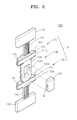
- FIGS. 2 and 3 are perspective views respectively showing the front and rear portions of the MEMS mirror 100 shown in FIG. 1 .
- the mirror scanner may include the MEMS mirror 100 formed with a MEMS structure, and an electromagnet portion 200 providing an electromagnetic driving force to the MEMS mirror 100.
- the MEMS mirror 100 may include an movable unit 110, a first spring unit 181 and a second spring unit 182 that elastically supports the movable unit 110, and a first fixing end 191 and a second fixing end 192 supporting the first and second spring units 181 and 182, respectively.
- the movable unit 110 may be pivoted by the electromagnetic driving force provided by the electromagnet portion 200, and may include one or more mirror portion(s) 120, a reinforcing rib 125 formed on at least one surface of the mirror portion 120, and a magnet frame portion 130 extending from the mirror portion 120.
- a permanent magnet 139 may be inserted in the magnet frame portion 130.
- the mirror portions 120 may include the first and second unit mirrors 121 and 122, which may in turn include the mirror surfaces 121a/121b and 122a/122b, respectively.
- the mirror surfaces 121a and 121b and 122a and 122b may be formed as thin metal films through a plating process or a deposition process, or can be formed by attaching an additional reflective film to the first and second unit mirrors 121 and 122.
- a distance between the first and second unit mirrors 121 and 122 may be determined in consideration of the installation space for the magnet frame portion 130.
- the mirror portion 120 is shown to include two unit mirrors 121 and 122.
- the present disclosure is so limited, and also contemplates a mirror portion 120 that include only one unit mirror or that includes three or more unit mirrors.
- the mirror portion 120 may pivots or oscillate with an oscillation period, which can range, for example, from hundreds to thousands of Hz about the rotating center axis (C in FIG. 3 ), as will be described in greater detail later.
- Stress due to the inertia of the oscillating mirror portion 120 may cause the mirror surfaces 121a and 121b and 122a and 122b to be deformed, and the deformation may become severe as the pivoting speed of the mirror portion 120 increases.
- the deformation of the mirror surfaces 121a, 121b, 122a, and 122b may change the position of the scanned light beam, and thus, result in the degradation of image quality.
- reinforcing rib 125 may be formed on at least a portion of the boundaries of the mirror surfaces 121a, 121b, 122a, and 122b to alleviate the deformation of the mirror surfaces.
- the reinforcing rib 125 may allow the mirror portion 120 to remain relatively thin while maintaining sufficient rigidity.
- the thinner profile of the mirror portion 120 may also contribute in the reduction of the moment of inertia of the movable unit 110, which may in turn result in the improvement of the high frequency performance of the movable unit 110, and may also reduce the consumption of power required to operate the mirror scanner.
- the reinforcing rib 125 may be formed on one or both surfaces of the mirror portion 120.
- the reinforcing rib 125 may be formed on one surface of the mirror portion 120 when the MEMS mirror 100 is fabricated using a silicon-on-insulator (SOI) substrate having a dual-layered structure, which will be described in greater detail later,.
- SOI silicon-on-insulator
- the reinforcing rib 125 may be formed on both surfaces of the mirror portion 120 through a substrate bonding process when, for example, the MEMS mirror 100 is fabricated using a substrate having a triple-layered structure.
- the reinforcing rib 125 may be formed on both surfaces of the mirror portion 120, and to be perpendicular to the rotating center axis C of the movable unit 110. Since the deformation of the mirror surfaces 121a, 121b, 122a, and 122b may occur in the direction that is perpendicular to the rotating center axis C of the movable unit 110, the deformation of the mirror surfaces can be reduced when the reinforcing rib 125 is formed perpendicular to the rotating center axis C of the movable unit 110.
- the magnet frame portion 130 may include a magnet frame 135 and a permanent magnet 139 that can be installed in the magnet frame 135.
- the magnet frame 135 may be located, e.g., between the first and second unit mirrors 121 and 122. With the magnet frame 135 located between the first and second unit mirrors 121 and 122, the first and second unit mirrors 121 and 122, the first and second spring units 181 and 182, and the first and second fixing ends 191 and 192 can be arranged symmetrically about the magnet frame 135.
- the magnet frame portion 130 having the above structure separates the first and second unit mirrors 121 and 122 from each other so that the electromagnet portion 200 can be positioned at the space between the light beams scanned by the first and second unit mirrors 121 and 122.
- the magnet frame 135 includes an opening 135a in which the permanent magnet 139 may be received.
- the opening 135a may be formed to extend parallel to the mirror surfaces 121a, 121b, 122a, and 122b, with which structure, the direction (M) of magnetic poles of the permanent magnet 139 being perpendicular to the mirror surfaces 121a, 121b, 122a, and 122b. That is, the magnetic pole direction M of the permanent magnet 139 may be parallel to the direction in which the permanent magnet 139 is received into the magnet frame 135.
- the permanent magnet 139 can be inserted so that the N pole of the permanent magnet 139 faces the electromagnet portion 200.
- the relationship between the magnetic pole direction M of the permanent magnet 139 and the electromagnet portion 200 will be described in greater detail later.
- the opening 135a may include a grip structure 136 on the side wall thereof, as shown in FIGS. 4A and 4B , so that the permanent magnet 139 can be supported in the magnet frame 135.
- a grip structure 136 on the side wall thereof, as shown in FIGS. 4A and 4B , so that the permanent magnet 139 can be supported in the magnet frame 135.
- FIG. 4A when a force 301 is applied to the sides of the grip structure 136, the permanent magnet 139 is able to move within the opening, and can thus be inserted into, or removed from, the magnet frame 135.
- FIG. 4B when the force is not applied to the grip structure 136, the grip structure 136 securely holds the permanent magnet 139.
- the grip structure 136 shown in FIGS. 4A and 4B is only an example, and can be modified into variety of other configurations.
- the first and second spring units 181 and 182 respectively connect the movable unit 110 to the first and second fixing ends 191 and 192, and elastically support the movable unit 110.
- the first and second spring units 181 and 182 may be formed in zigzagging shape.
- the zigzag shape may disperse the stress generated during the pivoting of the movable unit 110 in the limited space, and thus may reduce stress related failures.
- the elastic resilience of the first and second spring units 181 and 182 is a factor that determines a resonant frequency of the movable unit 110 with the moment of inertia of the movable unit 110. Therefore, the resonant frequency of the movable unit 110 can be adjusted by the appropriate design of the zigzag shape of the first and second spring units 181 and 182.
- the first and second fixing ends 191 and 192 support the first and second spring units 181 and 182.
- the first and second fixing ends 191 and 192 may also include holes (not shown) so as to facilitate assembling of the MEMS mirror 100 with other structures.
- the electromagnet portion 200 includes a yoke 210, and a coil 220 surrounding the yoke 210.
- the electromagnet portion 200 is designed to have a thickness T (see FIG. 10 ) that is less than the distance D between the first and second unit mirrors 121 and 122 so as not to interfere with the paths of the light beams to and from the first and second unit mirrors 121 and 122 (refer to L1 and L4 of FIG. 10 ), and is disposed between the parallel light beams L1 and L4 that are incident on the first and second unit mirrors 121 and 122 as shown in FIG. 10 .
- the yoke 210 defines a path of a magnetic flux (refer to B of FIG. 8 ), which is formed by the electric current flow in the coil 220.
- the yoke 210 may be formed of a soft magnetic material.
- the yoke 210 includes ends (refer to A1 and A2 of FIG. 8 ) that are spaced apart from, and face, each other, the magnetic flux exiting from both of the ends A1 and A2.
- the ends A1 and A2 of the yoke 210 are positioned adjacent to the permanent magnet 139, and the shapes of the ends A1 and A2 of the yoke 210 may vary depending on the shape of the permanent magnet 139.
- the ends A1 and A2 of the yoke 210 may be formed to be straight.
- the shape of the permanent magnet 139 and the ends of the yoke 210 however are not limited to the above example.
- ends A1 and A2 of the yoke 210 may be formed as coaxial cylindrical surfaces.
- a method of fabricating the MEMS mirror 100 will be described with reference to FIGS. 5, 6 , and 7A -to 7C .
- FIG. 5 is a side view of the MEMS mirror 100.
- a body of the MEMS mirror 100 may be formed of a silicon-on-insulator (SOI) wafer, which may be used to form most of the MEMS mirror 100 except for the permanent magnet 139 and/or the reflective surfaces of the mirrors.
- SOI wafer is a silicon substrate including an insulating layer in an intermediate portion thereof, and is an example of double-layered wafer.
- the body of the MEMS mirror 100 can be divided into an upper portion and a lower portion based on an insulating layer 105.
- the first and second unit mirrors 121 and 122 and the first and second spring units 181 and 182 may be formed with a first silicon layer above the insulating layer 105, and the reinforcing rib 125 may be formed with a second silicon layer under the insulating layer 105.
- the magnet frame 135 and the first and second fixing ends 191 and 192 may, for example, be formed with both of the first and second silicon layers.
- the body of the MEMS mirror 100 including the reinforcing rib 125, may be formed through a single wafer process.
- the body of the MEMS mirror 100 is formed using the SOI wafer, however, the present disclosure is not limited to the above example.
- the body of the MEMS mirror 100 may be formed by bonding two substrates.
- the reinforcing rib 125 may be formed on upper and lower portions of the first and second unit mirrors 121 and 122 using a triple-layered substrate.
- FIGS. 6 , and 7A through 7C illustrate processes of inserting the permanent magnet 139 into the magnet frame 135.
- FIG. 6 shows the permanent magnet 139, of which the installed position can be adjusted in upward and downward directions 305, in the body of the MEMS mirror 100
- FIGS. 7A through 7C illustrate processes of inserting the permanent magnet 139 into the magnet frame 135.
- a center of gravity of the entire movable unit 110 varies according to the position of the permanent magnet 139 within the magnet frame 135 due to the weight of the permanent magnet 139. Therefore, the center of gravity of the movable unit 110 can be made to coincide with the rotating center axis C' of the first and second spring units 181 and 182 by adjusting the position of the permanent magnet 139 in the upward and downward directions 305. That is, the rotating center axis C of the movable unit 110 and the rotating center axis C' of the first and second spring units 181 and 182 can be made to coincide with each other by adjusting the position of the permanent magnet 139 within the magnet frame 135.
- the rotating center axis C' of the first and second spring units 181 and 182 is the rotating center axis only with respect to the rotation of the first and second spring units 181 and 182. As described above, when the rotating center axis C of the movable unit 110 and the rotating center axis C' of the first and second spring units 181 and 182 coincide with each other, vibrations of the operation unit 110 during the pivoting of the movable unit 110 about the rotating center axis C can be reduced.
- the grip structure 136 disengages with the permanent magnet 139 (as also shown in FIG. 4A ), and thus, the permanent magnet 139 can be inserted into the magnet frame 135.
- the position of the permanent magnet 139 may be controlled using the assembling jig 310 so that the rotating center axis C of the movable unit 110 (refer to FIG. 3 ) and the rotating center axis C' of the first and second spring units 181 and 182 (refer to FIG. 6 ) can be made to coincide.
- the chuck 320 is retrieved so that the grip structure 136 engages with the permanent magnet 139 to support the permanent magnet 139 in place at the proper position.
- the permanent magnet 139 may be fixed in position within the magnet frame 135 using a fixing member 138, such as, e.g., epoxy.
- a fixing member 138 such as, e.g., epoxy.
- the center of gravity of the movable unit 110 can be adjusted by inserting the permanent magnet 139 in the magnet frame 135.
- the permanent magnet 139 can be held in position within the magnet frame 135 using the grip structure 136 formed in the magnet frame 135.
- FIGS. 8 through 11 illustrate the operations of the mirror scanner according to an embodiment.
- FIG. 8 illustrates the force applied to the permanent magnet 139 by the electromagnet portion 200
- FIG. 9 shows a range of scanning light beams according to the rotation of the mirror portion 120.
- FIG. 10 illustrates the light beams that are incident onto the mirror scanner
- FIG. 11 illustrates the light beams scanned by the mirror scanner according to the present embodiment.
- the end portions A1 and A2 of the yoke 210 face each other around the N pole of the permanent magnet 139.
- electric current i flows through the coil 220 of the electromagnet portion 200
- the magnetic flux B is induced in the yoke 210, and the magnetic flux B exits from the end portions A1 and A2 of the yoke 210.
- the electric current i flows in the direction shown in FIG. 8
- the magnetic flux B exits at the end portion A1 of the yoke 210 and enters the end portion A2 of the yoke 210. That is, the end portion A1 becomes N pole, and the end portion A2 becomes S pole.
- the magnetic pole direction M of the permanent magnet 139 is set with the N pole at the side facing the yoke 210 and the S pole at the opposite side.
- a repulsive force is applied to the permanent magnet 139 around the end portion A1 by the magnetic flux B of the electromagnet portion 200, and an attractive force is applied to the permanent magnet 139 around the end portion A2.
- the permanent magnet 139 pivots about the rotating center axis C in the clockwise direction.
- the forces applied to the permanent magnet 139 are also reversed, and as a result the permanent magnet 139 pivots about the rotating center axis C in the counter-clockwise direction.
- the pivoting direction of the permanent magnet 139 can be determined by controlling the direction of the current flow i in the electromagnet portion 200.
- the pivoting of the permanent magnet 139 and the magnet frame portion 130 directly results in pivoting of the mirror portion 120.
- the operating frequency of the current i supplied to the electromagnet portion 200 is the resonant frequency of the movable unit 110
- the movable unit 110 vibrates in a sine waveform in a resonance mode.
- the resonant frequency of the movable unit 110 may be determined by the relationship between the moment of inertia of the movable unit 110 and the elastic resilience of the first and second spring units 181 and 182.
- first and second incident light beams L1i and L2i are incident on the first unit mirror 121 that oscillates at the resonant frequency
- first and second reflected light beams L1r and L2r reflected by the first unit mirror 121 are scanned across within the scanning region ranges denoted as SR1 and SR2, respectively.
- the mirror scanner may include the first and second unit mirrors 121 and 122 (as shown, e.g., in FIG. 2 ), and thus, four light beams: first through fourth light beams L1, L2, L3, and L4 can be simultaneously scanned, as shown in FIGS. 10 and 11 . That is, the first and second light beams L1 and L2 may be reflected by the mirror surfaces 121a and 121b of the first unit mirror 121, and may thereby be scanned across the scanning region ranges SR1 and SR2 while the third and fourth light beams L3 and L4 may be reflected by the mirror surfaces 122a and 122b of the second unit mirror 122, and may thus be scanned across the scanning region ranges SR3 and SR4.
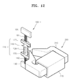
- FIG. 12 is a schematic diagram showing a structure of a mirror scanner according to another embodiment
- FIGS. 13 and 14 are perspective views showing the front and rear portions of a MEMS mirror 100-1 shown in FIG. 12 .
- the mirror scanner according to the embodiment is substantially the same as the mirror scanner according to the previous embodiment shown in FIGS. 1 through 11 except for a magnetic pole direction M of a permanent magnet 139-1.
- like elements are denoted by like reference numerals, and descriptions of the previously described like elements may not be repeated in detail.
- the mirror scanner may include a MEMS mirror 100-1, and the electromagnet portion 200 providing an electromagnetic driving force to the MEMS mirror 100-1.
- the MEMS mirror 100-1 may include a movable unit 110-1, the first and second spring units 181 and 182 elastically supporting the movable unit 110-1, and the first and second fixing ends 191 and 192 respectively supporting the first and second spring units 181 and 182.
- the movable unit 110-1 may include the mirror portion 120, the reinforcing rib 125 formed on at least one surface portion of the mirror portion 120, and a magnet frame portion 130-1 extending from the mirror portion 120.
- the permanent magnet 139-1 may be received in the magnet frame portion 130-1.
- the mirror portion 120 may include the first and second unit mirrors 121 and 122, each of which may in turn include on both surfaces thereof respective mirror surfaces 121a/121b, and 122a/122b.
- the mirror portion 120 may includes the reinforcing rib 125 for improving the rigidity of the mirror portion 120.
- the magnet frame 135-1 may include an opening 135a into which the permanent magnet 139-1 may be received.
- the opening 135a may be formed to extend parallel to the mirror surfaces 121a, 121b, 122a, and 122b.
- the magnetic pole direction M of the permanent magnet 139-1 may be parallel to the mirror surfaces 121a, 121b, 122a, and 122b, and may be perpendicular to the rotating center axis C (refer to FIG. 3 ). That is, while, in the embodiments shown in FIGS 1-11 , the magnetic poles of the permanent magnet 139 were seen from the view showing the wider surface of the MEMS mirror 100 (see FIG. 2 ), according to the embodiments shown in FIG. 13 , the poles of the permanent magnet 139-1 are shown when the permanent magnet 139-1 is seen from a side of the MEMS mirror 100-1.
- the arrangements of the MEMS mirror 100-1 and the electromagnet portion 200 may be different from those of the previous embodiments. That is, in the previous embodiment, the ends A1 and A2 of the yoke 210 face the larger surface of the MEMS mirror 100 when the MEMS mirror 100 is in the initial non-operating position as shown in FIG. 1 . However, according to the embodiments of FIG. 13 , the ends A1 and A2 of the yoke 210 face the side of the MEMS mirror 100-1 when the MEMS mirror 100-1 is in the initial non-operating position as shown in FIG. 12 .
- FIG. 15 illustrates the light beams incident on the mirror scanner of the embodiments of FIGS. 12-14
- FIG. 16 illustrates the light beams scanned by the mirror scanner.
- the mirror scanner since the mirror scanner includes four mirror surfaces 121a, 121b, 122a, and 122b, four light beams L1, L2, L3, and L4 may simultaneously be scanned. Since the electromagnet portion 200 is located at the side of the MEMS mirror 100-1, the electromagnet portion 200 may be placed not to interfere with the light paths of the incident light beams L1i and L2i or the reflected light beams L1r and L2r as shown in FIG. 16 , and accordingly, the installation space of the electromagnet portion 200 can easily be ensured.
- FIG. 17 is a schematic diagram showing a structure of a mirror scanner according to another embodiment, and FIG. 18 shows parallel light beams incident on the mirror scanner of FIG. 17 .
- the mirror scanner of the embodiments shown in FIG. 17 may be substantially the same as the mirror scanner shown in FIGS. 1 through 11 , except that the magnet frame portion 130 is disposed below the mirror portion 120-1.
- like elements are denoted by like reference numerals, and the detailed descriptions of the like elements already described may not be repeated.
- the mirror scanner may include a MEMS mirror 100-2, and an electromagnet portion 200-1 providing an electromagnetic driving force to the MEMS mirror 100-2.
- the MEMS mirror 100-2 may include a movable unit 110-2, the first and second spring units 181 and 182 elastically supporting the movable unit 110-2, and the first and second fixing ends 191 and 192 respectively supporting the first and second spring units 181 and 182.
- the movable unit 110-2 may include the mirror portion 120-1 in which first and second unit mirrors 121-1 and 122-1 are fixedly coupled to each other via a rigid connection unit 126, and the magnet frame portion 130 disposed to extend from the mirror portion 120-1.
- a rigid connection unit 126 is disposed between the first and second unit mirrors 121-1 and 122-1, and determines a predetermined distance between the mirrors.
- the rigid connection unit 126 may be of sufficient rigidity so as not to twist, and thus, the first and second unit mirrors 121-1 and 122-1 may pivot simultaneously with respect to each other.
- the electromagnet portion 200-1 is also disposed on the same side the mirror portion 120-1. That is, in contrast to the previous embodiments, there is no need to dispose the electromagnet portion 200-1 between the first and second unit mirrors 121-1 and 122-1, and thus a sufficient space for the installation of the electromagnet portion 200-1 can be ensured. Moreover, as shown in FIG.
- the end portions of a yoke 210-1 may be stepped or curved to be adjacent to the magnet frame portion 130 while the remaining portion of the electromagnet portion 200-1 (except for the end portions of the yoke 210-1) can be arranged to be out of and away from the optical paths of the incident or reflected light beams L1, L2, L3, and L4.
- the thickness of the electromagnet portion 200-1 since a sufficient space for installing the electromagnet portion 200-1 can be ensured, there may not be a limitation for the thickness of the electromagnet portion 200-1.
- the magnetic pole direction of the permanent magnet that is inserted into the magnet frame portion 130 may be either perpendicular or parallel to the mirror surfaces.
- the end portions of the yoke 210-1 may face either the broad face of the MEMS mirror 100-2 or the side of the MEMS mirror 100-2 according to the magnetic pole direction of the permanent magnet.
- FIG. 19 is a schematic diagram showing a structure of a mirror scanner according to another alternative embodiments.
- the mirror scanner of the embodiment comprises a MEMS mirror 100-3 which may be substantially the same as the MEMS mirror shown in FIGS. 17 and 18 , except for the arrangement of a magnet frame portion 130-2.
- the magnet frame portion 130-2 of the present embodiment includes a first magnet frame 131 located between the mirror portion 120-1 and the first spring unit 181, and a second magnet frame 132 located between the mirror portion 120-1 and the second spring unit 182.
- Each of the first and second magnet frames 131 and 132 may include a first electromagnet portion and a second electromagnet portion (not shown). Since the first and second magnet frames 131 and 132 are each disposed to extend from the mirror portion 120-1, both of the corresponding first and second electromagnet portions may also be disposed away from the mirror portion 120-1, similarly with the electromagnet portion 200-1 shown in FIG. 17 . With the above described structure, as the first and second magnet frames 131 and 132 are symmetrically disposed about the mirror portion 120-1, the driving property of the MEMS mirror 100-3 can be improved.
- FIG. 20 is a schematic diagram showing a structure of a mirror scanner according to other alternative embodiments.
- the mirror scanner of the present embodiment is substantially the same as the mirror scanner shown in FIG. 19 , except that the magnet frame portion 130-2 and the mirror portion 120-1 are elastically supported with respect to one another.
- the MEMS mirror 100-4 may include a first sub-spring unit 141 between the mirror portion 120-1 and the first magnet frame 131, and a second sub-spring unit 142 between the mirror portion 120-1 and the second magnet frame 132.
- first magnet frame 131 is elastically supported by a first spring unit 181-1 and the first fixing end 191 while the second magnet frame 132 is elastically supported by the second spring unit 182-1 and the second fixing end 192.
- the magnet frame portion 130-2 and the mirror portion 120-1 may be in different resonance modes from each other. That is, the resonance mode of the magnet frame portion 130-2 is mainly in a first resonance frequency that is determined by the moment of inertia of the magnet frame portion 130-2 itself and the elastic resilience of the first and second spring units 181-1 and 181-2. In addition, the resonance mode of the mirror portion 120-1 is mainly in a second resonance frequency that is determined by the moment of inertia of the mirror portion 120-1 and the elastic resilience of the first and second sub-spring units 141 and 142.
- the first resonance frequency may be set to be greater than the second resonance frequency while the magnet frame portion 130-2 is excited at the second resonance frequency.
- the mirror portion 120-1 resonates at the second resonance frequency due to the vibration of the magnet frame portion 130-2.
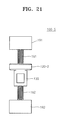
- FIG. 21 is a schematic diagram showing the structure of a mirror scanner 100-5 according yet other alternative embodiments, and FIG. 22 shows light beams that are obliquely incident on the mirror scanner of FIG. 21 .
- the mirror scanner 100-5 may be substantially the same as the mirror scanner shown in FIGS. 1 through 11 , except that a mirror portion 120-2 includes only one unit mirror in each face of the mirror portion 120-2.
- the mirror portion 120-2 includes one unit mirror in each face thereof, in order to scan four light beams simultaneously, two light beams L1 and L4, and two light beams L2 and L3 are made to be incident upon the mirror surfaces formed on the respective surfaces of the mirror portion 120-2 at an oblique incident angle as shown in FIG. 22 .
- the light beams are obliquely incident on the mirror surfaces, a plurality of light beams can be reflected in different light scanning paths from each other even if the mirror surfaces of the mirror portion 120-2 are relatively small.
- FIG. 23 shows an image forming apparatus including an optical scanning unit 500 according to one or more embodiments described herein.
- the image forming apparatus may include the optical scanning unit 500, developing units 600, photosensitive drums 700, charging rollers 701, an intermediate transfer belt 800, a transfer roller 805, and a fusing unit 900.
- the optical scanning unit 500 scans light beams L that are modulated according to image information onto the photosensitive drum 700.
- the photosensitive drum 700 is an example of a photosensitive medium, One skilled in the art would however appreciate that a photosensitive belt (not shown) can be another example of the photosensitive medium.
- the photosensitive drum 700 may, for example, be fabricated by forming a photosensitive layer of a predetermined thickness on an outer circumferential surface of a cylindrical metal pipe. An outer circumferential surface of the photosensitive drum 700 is a scan surface upon which the light beams L from the optical scanning unit 500 are incident.
- the charging roller 701 charges the outer circumferential surface of the photosensitive drum 700 to a uniform electric potential by applying a charging bias Vc while rotating in association with the outer circumferential surface of the photosensitive drum 700.
- a corona charger (not shown) may be used instead of the charging roller 701.
- the developing unit 600 supplies toner to the photosensitive drum 700, e.g., under a developing bias applied between the developing unit 600 and the photosensitive drum 700 to develop the electrostatic latent image into a visible toner image on the photosensitive drum 700.
- the toner image formed on the photosensitive drum 700 is transferred to the intermediate transfer belt 800.
- the toner image is transferred from the intermediate transfer belt 800 to a printing medium P that is conveyed between the transfer roller 805 and the intermediate transfer belt 800, for example, by the application of a transferring bias to the transfer roller 805.
- the toner image transferred onto the printing medium P is fused onto the printing medium P by, for example, heat and/or pressure applied from the fusing unit 900, completing the image forming operation.
- the optical scanning unit 500, the developing unit 600, and the photosensitive drum 700 may be provided as units corresponding to several colors.
- the optical scanning unit 500 scans four light beams respectively on the four photosensitive drums 700 to form electrostatic latent images corresponding to black (K), magenta (M), yellow (Y) and cyan (C) image information on the four photosensitive drums 700.
- Four developing units 600 provide the photosensitive drums 700 with toners of K, M, Y and C colors to develop the K, M, Y and C electrostatic latent image into the respective toner images.
- the K, M, Y and C toner images are transferred onto the intermediate transfer belt 800 to overlap with each other, and the overlapped color toner image is in turn transferred to the printing medium P.
- FIG. 24 shows an example of the optical scanning unit 500 adopted in the image forming apparatus of FIG. 23 in greater detail.
- the optical scanning unit 500 may include light sources 520', a mirror scanner including a MEMS mirror 100, a plurality of optical path converting members 530, and a focusing optics 540, and these optical elements may be received in a housing 510, which includes windows 511.
- the mirror scanner included in the optical scanning unit 500 may include the MEMS mirror 100 having four mirror surfaces, e.g., as previously described in reference to FIGS. 1 through 11 .
- the light source 520 each irradiates two light beams L in parallel onto a mirror surface of the respective face of the MEMS mirror 100.
- Optical paths of the light beams L are changed by the plurality of optical path converting members 530 to direct the light beams L toward the photosensitive drums 700K, 700Y, 700M and 700C.
- the focusing optics 540 are disposed on the optical paths of the light beams L, which proceed toward the photosensitive drums 700K, 700Y, 700M and 700C, and respectively focus the light beams L on the photosensitive drums 700K, 700Y, 700M and 700C. If the MEMS mirror 100 exhibits sinusoidal oscillation, the optical paths may need to be compensated in order that the light beams L that are deflected by the mirror scanner 100 can be scanned onto the photosensitive drums 700K, 700Y, 700M, and 700C at a uniform velocity.
- the focusing optics 540 may be a sine wave compensation lenses that compensate for the deflected light beams to have arcsinusoidal forms so that the light beams deflected by the mirror scanner 100 can be scanned onto the photosensitive drums 700K, 700Y, 700M, and 700C at a uniform velocity.
- FIG. 25 shows another embodiment of an optical scanning unit 500-1 that can be adapted in the image forming apparatus of FIG. 23 .
- the optical scanning unit 500-1 may include the light sources 520, a mirror scanner including a MEMS mirror 100-5, the plurality of optical path converting members 530 and the focusing optics 540, supported in the housing 510 that includes the windows 511.
- the mirror scanner of the optical scanning unit 500-1 may include the MEMS mirror 100-5 having two mirror surfaces, e.g., one on each face, for example, similar to those previously described in reference to FIGS. 21 and 22 .
- the light source 520 may each irradiates two light beams L onto a mirror surface on the respective face of the MEMS mirror 100-5 such that the light beams L are incident upon the mirror surface at an oblique angle.
- Optical paths of the light beams L are changed by the plurality of optical path converting members 530 to direct the light beams L toward the photosensitive drums 700K, 700Y, 700M and 700C.
- the focusing optics 540 are disposed on the respective optical paths of the light beams L, which proceed toward the photosensitive drums 700K, 700Y, 700M and 700C to focus the respective light beams L on the corresponding one of the photosensitive drums 700K, 700Y, 700M, and 700C.
- the focusing optics 540 may compensate for the deflected light beams L to have arcsinusoidal forms so that the light beams L can be scanned at a uniform velocity.
- a compensation lens (not shown), which can compensate for distortion that can be caused by the oblique irradiation of the light beams L, may further be disposed between the mirror scanner 100-5 and the focusing optics 540.
- the scanning of light beams is performed using an MEMS mirror that is driven by an electromagnetic force, the printing speed can be improved over the conventional deflection method that uses polygon mirrors, and noise can also be reduced.
- the MEMS mirror since the MEMS mirror includes mirror surfaces on both surfaces thereof, a plurality of light beams can be scanned simultaneously even when the mirror surfaces are made relatively small. Therefore, the performance degradation or dynamic deformation when the mirror surfaces increase in size to allow simultaneous scanning of a plurality of light beams attendant conventional art, can be mitigated.
Landscapes
- Physics & Mathematics (AREA)
- General Physics & Mathematics (AREA)
- Optics & Photonics (AREA)
- Electromagnetism (AREA)
- Micromachines (AREA)
- Mechanical Optical Scanning Systems (AREA)
- Mechanical Light Control Or Optical Switches (AREA)
- Laser Beam Printer (AREA)
- Facsimile Scanning Arrangements (AREA)
Applications Claiming Priority (1)
| Application Number | Priority Date | Filing Date | Title |
|---|---|---|---|
| KR1020080081858A KR101279441B1 (ko) | 2008-08-21 | 2008-08-21 | 멤스 미러, 미러 스캐너, 광주사 유닛 및 광주사 유닛을 채용한 화상형성장치 |
Publications (3)
| Publication Number | Publication Date |
|---|---|
| EP2157467A2 true EP2157467A2 (fr) | 2010-02-24 |
| EP2157467A3 EP2157467A3 (fr) | 2012-01-25 |
| EP2157467B1 EP2157467B1 (fr) | 2013-09-11 |
Family
ID=41426354
Family Applications (1)
| Application Number | Title | Priority Date | Filing Date |
|---|---|---|---|
| EP09165739.5A Not-in-force EP2157467B1 (fr) | 2008-08-21 | 2009-07-17 | Balayeur de miroir, unité de balayage optique et appareil de formation d'images incluant l'unité de balayage optique |
Country Status (5)
| Country | Link |
|---|---|
| US (1) | US8570633B2 (fr) |
| EP (1) | EP2157467B1 (fr) |
| JP (1) | JP5506287B2 (fr) |
| KR (1) | KR101279441B1 (fr) |
| CN (1) | CN101655602B (fr) |
Cited By (5)
| Publication number | Priority date | Publication date | Assignee | Title |
|---|---|---|---|---|
| WO2014177133A1 (fr) * | 2013-04-30 | 2014-11-06 | Scansonic Mi Gmbh | Dispositif scanner |
| CN104834161A (zh) * | 2014-02-07 | 2015-08-12 | 光宝科技股份有限公司 | 投影装置及其控制方法 |
| JP2016033613A (ja) * | 2014-07-31 | 2016-03-10 | 株式会社豊田中央研究所 | Mems装置 |
| EP3650908A4 (fr) * | 2017-07-06 | 2021-04-07 | Hamamatsu Photonics K.K. | Dispositif optique |
| EP4394479A1 (fr) * | 2022-12-29 | 2024-07-03 | Silicon Austria Labs GmbH | Dispositif à micro-miroirs et procédé de fonctionnement d'un dispositif à micro-miroirs |
Families Citing this family (37)
| Publication number | Priority date | Publication date | Assignee | Title |
|---|---|---|---|---|
| IL165212A (en) | 2004-11-15 | 2012-05-31 | Elbit Systems Electro Optics Elop Ltd | Device for scanning light |
| JP5659642B2 (ja) * | 2010-09-10 | 2015-01-28 | セイコーエプソン株式会社 | 光スキャナー、光スキャナーの製造方法、および画像形成装置 |
| US9204129B2 (en) * | 2010-09-15 | 2015-12-01 | Perceptron, Inc. | Non-contact sensing system having MEMS-based light source |
| CN103180772A (zh) * | 2010-11-24 | 2013-06-26 | 日本电气株式会社 | 光学扫描设备 |
| US9651417B2 (en) | 2012-02-15 | 2017-05-16 | Apple Inc. | Scanning depth engine |
| AU2013237061B2 (en) | 2012-03-22 | 2015-11-26 | Apple Inc. | Gimbaled scanning mirror array |
| WO2013175663A1 (fr) * | 2012-05-22 | 2013-11-28 | 日本電気株式会社 | Élément de balayage optique et dispositif de balayage optique |
| DE112013003679B4 (de) | 2012-07-26 | 2023-05-04 | Apple Inc. | Dual-Achsen-Scanspiegel und Verfahren zum Scannen |
| KR20150063540A (ko) | 2012-10-23 | 2015-06-09 | 애플 인크. | 마이크로 기계 디바이스의 제조 |
| JP5768803B2 (ja) * | 2012-11-15 | 2015-08-26 | 株式会社豊田中央研究所 | Mems装置 |
| JP5976132B2 (ja) * | 2013-02-08 | 2016-08-23 | パイオニア株式会社 | アクチュエータ |
| CN104924776A (zh) * | 2014-03-17 | 2015-09-23 | 联想(北京)有限公司 | 一种打印设备的激光扫描单元 |
| JP6287584B2 (ja) * | 2014-05-27 | 2018-03-07 | 株式会社Jvcケンウッド | Mems光スキャナ |
| US9784838B1 (en) | 2014-11-26 | 2017-10-10 | Apple Inc. | Compact scanner with gimbaled optics |
| US9835853B1 (en) | 2014-11-26 | 2017-12-05 | Apple Inc. | MEMS scanner with mirrors of different sizes |
| US9798135B2 (en) | 2015-02-16 | 2017-10-24 | Apple Inc. | Hybrid MEMS scanning module |
| US9703096B2 (en) | 2015-09-30 | 2017-07-11 | Apple Inc. | Asymmetric MEMS mirror assembly |
| US9897801B2 (en) | 2015-09-30 | 2018-02-20 | Apple Inc. | Multi-hinge mirror assembly |
| JP6724663B2 (ja) * | 2016-09-01 | 2020-07-15 | 船井電機株式会社 | スキャナミラー |
| US10488652B2 (en) | 2016-09-21 | 2019-11-26 | Apple Inc. | Prism-based scanner |
| JP6884322B2 (ja) | 2016-10-31 | 2021-06-09 | 国立大学法人福井大学 | 2次元光走査ミラー装置の製造方法 |
| WO2019172307A1 (fr) * | 2018-03-09 | 2019-09-12 | パイオニア株式会社 | Réflecteur à actionneur, scanner optique et actionneur de miroir |
| CN108873368A (zh) * | 2018-08-02 | 2018-11-23 | 西安知微传感技术有限公司 | 一种抑制激光散斑的方法及mems微振镜 |
| US10422881B1 (en) * | 2018-12-07 | 2019-09-24 | Didi Research America, Llc | Mirror assembly for light steering |
| US11181621B2 (en) | 2018-12-07 | 2021-11-23 | Beijing Voyager Technology Co., Ltd. | Mirror assembly for light steering |
| US11119195B2 (en) | 2018-12-07 | 2021-09-14 | Beijing Voyager Technology Co., Ltd. | Mirror assembly for light steering |
| WO2020117287A1 (fr) | 2018-12-07 | 2020-06-11 | Didi Research America, Llc | Ensemble miroir pour direction de lumière |
| CN109683308B (zh) * | 2019-02-01 | 2024-07-16 | 西安知微传感技术有限公司 | 一种降低摇摆运动的电磁驱动振镜 |
| CN109633893B (zh) * | 2019-02-01 | 2024-05-14 | 西安知微传感技术有限公司 | 一种电磁驱动振镜 |
| US11493609B2 (en) | 2019-03-01 | 2022-11-08 | Beijing Voyager Technology Co., Ltd. | MEMS device with integrated mirror position sensor |
| US11262575B2 (en) * | 2019-03-01 | 2022-03-01 | Beijing Voyager Technology Co., Ltd. | MEMS package with double-sided mirror |
| WO2020213623A1 (fr) * | 2019-04-19 | 2020-10-22 | パイオニア株式会社 | Dispositif mobile |
| CN114208006B (zh) | 2019-08-18 | 2024-10-29 | 苹果公司 | 具有电磁致动的力平衡微镜 |
| US20210173177A1 (en) * | 2019-12-05 | 2021-06-10 | Panasonic Automotive Systems Company Of America, Division Of Panasonic Corporation Of North America | Magnetic mirror movement |
| DE102021200018A1 (de) * | 2021-01-05 | 2022-07-07 | Robert Bosch Gesellschaft mit beschränkter Haftung | Mikromechanisches Schwingungssystem |
| US20230204829A1 (en) * | 2021-12-27 | 2023-06-29 | Tdk Taiwan Corp. | Optical element driving mechanism |
| CN120143439A (zh) * | 2023-12-11 | 2025-06-13 | 广东粤港澳大湾区国家纳米科技创新研究院 | Mems振镜制备方法 |
Family Cites Families (24)
| Publication number | Priority date | Publication date | Assignee | Title |
|---|---|---|---|---|
| JP2001290099A (ja) * | 2000-04-05 | 2001-10-19 | Fujitsu Ltd | ガルバノミラー装置 |
| US6831765B2 (en) * | 2001-02-22 | 2004-12-14 | Canon Kabushiki Kaisha | Tiltable-body apparatus, and method of fabricating the same |
| JP2002321196A (ja) * | 2001-02-22 | 2002-11-05 | Canon Inc | マイクロ構造体、マイクロ力学量センサ、マイクロアクチュエータ、マイクロ光偏向器、光走査型ディスプレイ、及びそれらの製造方法 |
| US6897990B2 (en) * | 2001-12-28 | 2005-05-24 | Canon Kabushiki Kaisha | Rocking member apparatus |
| JP3848249B2 (ja) * | 2001-12-28 | 2006-11-22 | キヤノン株式会社 | 揺動体装置 |
| JP2004021133A (ja) | 2002-06-20 | 2004-01-22 | Canon Inc | 走査光学装置 |
| US7259900B2 (en) * | 2002-11-08 | 2007-08-21 | Texas Instruments Incorporated | Multilayer torsional hinged mirror with a recessed drive/sensing permanent magnet |
| JP2005091966A (ja) | 2003-09-19 | 2005-04-07 | Canon Inc | 光走査装置およびそれを用いたカラー画像形成装置 |
| JP2005181714A (ja) | 2003-12-19 | 2005-07-07 | Canon Inc | 偏向走査装置 |
| JP4331086B2 (ja) | 2004-10-28 | 2009-09-16 | セイコーインスツル株式会社 | 電磁アクチュエータおよびそれを用いた光デバイス |
| JP2006126646A (ja) | 2004-10-29 | 2006-05-18 | Canon Inc | 画像形成装置 |
| JP4673115B2 (ja) * | 2005-04-07 | 2011-04-20 | 株式会社リコー | 光走査装置、およびそれを用いた画像形成装置 |
| US20070053045A1 (en) * | 2005-04-28 | 2007-03-08 | Texas Instruments Incorporated | Two sided torsional hinged mirror and method of manufacturing |
| JP4970865B2 (ja) * | 2005-07-28 | 2012-07-11 | 株式会社リコー | 偏向装置、光走査装置及び画像形成装置 |
| JP5073945B2 (ja) * | 2005-12-26 | 2012-11-14 | 株式会社リコー | 光走査装置・画像形成装置 |
| JP5441309B2 (ja) * | 2006-02-13 | 2014-03-12 | キヤノン株式会社 | 揺動体装置、及び光偏向装置 |
| JP4881073B2 (ja) * | 2006-05-30 | 2012-02-22 | キヤノン株式会社 | 光偏向器、及びそれを用いた光学機器 |
| JP4963399B2 (ja) * | 2006-10-23 | 2012-06-27 | キヤノン株式会社 | 画像形成装置 |
| JP5064864B2 (ja) * | 2007-04-02 | 2012-10-31 | キヤノン株式会社 | 光偏向装置、画像形成装置、及び光偏向装置の駆動方法 |
| JP4265675B2 (ja) * | 2007-04-06 | 2009-05-20 | トヨタ自動車株式会社 | 内燃機関の制御装置 |
| JP2008299297A (ja) * | 2007-06-04 | 2008-12-11 | Canon Inc | 揺動体装置、及び揺動体装置の振動系の駆動制御方法 |
| CN100451728C (zh) | 2007-07-06 | 2009-01-14 | 清华大学 | 带压阻传感器的微型二维扫描镜 |
| JP2009031643A (ja) * | 2007-07-30 | 2009-02-12 | Canon Inc | 揺動体装置、光偏向器およびそれを用いた画像形成装置 |
| JP4974846B2 (ja) * | 2007-10-26 | 2012-07-11 | キヤノン株式会社 | 光学走査装置及びそれを備える画像形成装置 |
-
2008
- 2008-08-21 KR KR1020080081858A patent/KR101279441B1/ko not_active Expired - Fee Related
-
2009
- 2009-07-17 EP EP09165739.5A patent/EP2157467B1/fr not_active Not-in-force
- 2009-07-29 US US12/511,688 patent/US8570633B2/en not_active Expired - Fee Related
- 2009-08-21 JP JP2009192465A patent/JP5506287B2/ja not_active Expired - Fee Related
- 2009-08-21 CN CN200910167370.3A patent/CN101655602B/zh not_active Expired - Fee Related
Cited By (17)
| Publication number | Priority date | Publication date | Assignee | Title |
|---|---|---|---|---|
| WO2014177133A1 (fr) * | 2013-04-30 | 2014-11-06 | Scansonic Mi Gmbh | Dispositif scanner |
| US9389417B2 (en) | 2013-04-30 | 2016-07-12 | Scansonic Mi Gmbh | Scanner device |
| CN104834161A (zh) * | 2014-02-07 | 2015-08-12 | 光宝科技股份有限公司 | 投影装置及其控制方法 |
| JP2016033613A (ja) * | 2014-07-31 | 2016-03-10 | 株式会社豊田中央研究所 | Mems装置 |
| US11209260B2 (en) | 2017-07-06 | 2021-12-28 | Hamamatsu Photonics K.K. | Optical module having high-accuracy spectral analysis |
| US11054309B2 (en) | 2017-07-06 | 2021-07-06 | Hamamatsu Photonics K.K. | Optical module |
| US11067380B2 (en) | 2017-07-06 | 2021-07-20 | Hamamatsu Photonics K.K. | Optical module |
| US11187579B2 (en) | 2017-07-06 | 2021-11-30 | Hamamatsu Photonics K.K. | Optical device |
| EP3650908A4 (fr) * | 2017-07-06 | 2021-04-07 | Hamamatsu Photonics K.K. | Dispositif optique |
| US11624605B2 (en) | 2017-07-06 | 2023-04-11 | Hamamatsu Photonics K.K. | Mirror unit and optical module |
| US11629946B2 (en) | 2017-07-06 | 2023-04-18 | Hamamatsu Photonics K.K. | Mirror unit and optical module |
| US11629947B2 (en) | 2017-07-06 | 2023-04-18 | Hamamatsu Photonics K.K. | Optical device |
| US11635290B2 (en) | 2017-07-06 | 2023-04-25 | Hamamatsu Photonics K.K. | Optical module |
| US11879731B2 (en) | 2017-07-06 | 2024-01-23 | Hamamatsu Photonics K.K. | Mirror unit and optical module |
| US12152878B2 (en) | 2017-07-06 | 2024-11-26 | Hamamatsu Photonics K.K. | Mirror unit and optical module |
| US12298132B2 (en) | 2017-07-06 | 2025-05-13 | Hamamatsu Photonics K.K. | Optical device |
| EP4394479A1 (fr) * | 2022-12-29 | 2024-07-03 | Silicon Austria Labs GmbH | Dispositif à micro-miroirs et procédé de fonctionnement d'un dispositif à micro-miroirs |
Also Published As
| Publication number | Publication date |
|---|---|
| EP2157467A3 (fr) | 2012-01-25 |
| EP2157467B1 (fr) | 2013-09-11 |
| US8570633B2 (en) | 2013-10-29 |
| KR101279441B1 (ko) | 2013-07-05 |
| JP2010049259A (ja) | 2010-03-04 |
| CN101655602B (zh) | 2015-04-01 |
| CN101655602A (zh) | 2010-02-24 |
| KR20100023210A (ko) | 2010-03-04 |
| JP5506287B2 (ja) | 2014-05-28 |
| US20100046054A1 (en) | 2010-02-25 |
Similar Documents
| Publication | Publication Date | Title |
|---|---|---|
| EP2157467B1 (fr) | Balayeur de miroir, unité de balayage optique et appareil de formation d'images incluant l'unité de balayage optique | |
| US7408690B2 (en) | Actuator, optical scanner, and image forming apparatus | |
| JP4673115B2 (ja) | 光走査装置、およびそれを用いた画像形成装置 | |
| JP5228331B2 (ja) | 光走査装置、画像形成装置、および多色対応の画像形成装置 | |
| JP4965284B2 (ja) | 光走査装置・画像形成装置 | |
| JP2011107675A (ja) | 光偏向素子、光偏向器、及び画像形成装置 | |
| JP2007171852A (ja) | 光走査装置・画像形成装置 | |
| JP5041835B2 (ja) | 光走査装置及び画像形成装置 | |
| JP2011017916A (ja) | 光偏向器、光走査装置、画像形成装置及び画像投影装置 | |
| JP4983266B2 (ja) | 光学デバイス、光スキャナ、および画像形成装置 | |
| US7911669B2 (en) | Optical scanning device and image forming apparatus using the same | |
| JP2012093431A (ja) | 光偏向器、光走査装置、画像形成装置及び画像投影装置 | |
| JP2009069340A (ja) | アクチュエータ、光スキャナ、および画像形成装置 | |
| JP4525652B2 (ja) | アクチュエータ、光スキャナ、および画像形成装置 | |
| JP5404342B2 (ja) | 光学走査装置及びそれを用いた画像形成装置 | |
| JP6157128B2 (ja) | 光走査装置及び画像形成装置 | |
| JP2011095458A (ja) | 光走査装置及びこれを備えた画像形成装置 | |
| JP2007025009A (ja) | 光スキャナユニット及びこれを備えた画像形成装置 | |
| JP5470872B2 (ja) | 画像形成装置 | |
| JP2009069341A (ja) | アクチュエータ、光スキャナ、および画像形成装置 | |
| JP2004029113A (ja) | 光走査装置および画像形成装置 | |
| JP2009031364A (ja) | 光走査装置及びこれを搭載する画像形成装置 | |
| JP2002098926A (ja) | 光走査装置 | |
| JP2009205175A (ja) | 画像形成装置 | |
| JP2008009028A (ja) | 光走査装置及び該装置を用いた画像形成装置 |
Legal Events
| Date | Code | Title | Description |
|---|---|---|---|
| PUAI | Public reference made under article 153(3) epc to a published international application that has entered the european phase |
Free format text: ORIGINAL CODE: 0009012 |
|
| AK | Designated contracting states |
Kind code of ref document: A2 Designated state(s): AT BE BG CH CY CZ DE DK EE ES FI FR GB GR HR HU IE IS IT LI LT LU LV MC MK MT NL NO PL PT RO SE SI SK SM TR |
|
| AX | Request for extension of the european patent |
Extension state: AL BA RS |
|
| PUAL | Search report despatched |
Free format text: ORIGINAL CODE: 0009013 |
|
| AK | Designated contracting states |
Kind code of ref document: A3 Designated state(s): AT BE BG CH CY CZ DE DK EE ES FI FR GB GR HR HU IE IS IT LI LT LU LV MC MK MT NL NO PL PT RO SE SI SK SM TR |
|
| AX | Request for extension of the european patent |
Extension state: AL BA RS |
|
| RIC1 | Information provided on ipc code assigned before grant |
Ipc: H04N 1/04 20060101ALI20111222BHEP Ipc: G02B 26/08 20060101AFI20111222BHEP Ipc: G02B 26/10 20060101ALI20111222BHEP |
|
| 17P | Request for examination filed |
Effective date: 20120622 |
|
| RAP1 | Party data changed (applicant data changed or rights of an application transferred) |
Owner name: SAMSUNG ELECTRONICS CO., LTD. |
|
| RIC1 | Information provided on ipc code assigned before grant |
Ipc: H04N 1/12 20060101ALN20130515BHEP Ipc: G02B 26/10 20060101ALI20130515BHEP Ipc: H04N 1/113 20060101ALN20130515BHEP Ipc: G02B 26/08 20060101AFI20130515BHEP |
|
| GRAP | Despatch of communication of intention to grant a patent |
Free format text: ORIGINAL CODE: EPIDOSNIGR1 |
|
| INTG | Intention to grant announced |
Effective date: 20130625 |
|
| GRAS | Grant fee paid |
Free format text: ORIGINAL CODE: EPIDOSNIGR3 |
|
| GRAA | (expected) grant |
Free format text: ORIGINAL CODE: 0009210 |
|
| AK | Designated contracting states |
Kind code of ref document: B1 Designated state(s): AT BE BG CH CY CZ DE DK EE ES FI FR GB GR HR HU IE IS IT LI LT LU LV MC MK MT NL NO PL PT RO SE SI SK SM TR |
|
| REG | Reference to a national code |
Ref country code: GB Ref legal event code: FG4D |
|
| REG | Reference to a national code |
Ref country code: CH Ref legal event code: EP |
|
| REG | Reference to a national code |
Ref country code: AT Ref legal event code: REF Ref document number: 631947 Country of ref document: AT Kind code of ref document: T Effective date: 20130915 |
|
| REG | Reference to a national code |
Ref country code: IE Ref legal event code: FG4D |
|
| REG | Reference to a national code |
Ref country code: DE Ref legal event code: R096 Ref document number: 602009018682 Country of ref document: DE Effective date: 20131107 |
|
| PG25 | Lapsed in a contracting state [announced via postgrant information from national office to epo] |
Ref country code: CY Free format text: LAPSE BECAUSE OF FAILURE TO SUBMIT A TRANSLATION OF THE DESCRIPTION OR TO PAY THE FEE WITHIN THE PRESCRIBED TIME-LIMIT Effective date: 20130821 Ref country code: NO Free format text: LAPSE BECAUSE OF FAILURE TO SUBMIT A TRANSLATION OF THE DESCRIPTION OR TO PAY THE FEE WITHIN THE PRESCRIBED TIME-LIMIT Effective date: 20131211 Ref country code: HR Free format text: LAPSE BECAUSE OF FAILURE TO SUBMIT A TRANSLATION OF THE DESCRIPTION OR TO PAY THE FEE WITHIN THE PRESCRIBED TIME-LIMIT Effective date: 20130911 Ref country code: LT Free format text: LAPSE BECAUSE OF FAILURE TO SUBMIT A TRANSLATION OF THE DESCRIPTION OR TO PAY THE FEE WITHIN THE PRESCRIBED TIME-LIMIT Effective date: 20130911 Ref country code: SE Free format text: LAPSE BECAUSE OF FAILURE TO SUBMIT A TRANSLATION OF THE DESCRIPTION OR TO PAY THE FEE WITHIN THE PRESCRIBED TIME-LIMIT Effective date: 20130911 |
|
| REG | Reference to a national code |
Ref country code: NL Ref legal event code: VDEP Effective date: 20130911 |
|
| REG | Reference to a national code |
Ref country code: AT Ref legal event code: MK05 Ref document number: 631947 Country of ref document: AT Kind code of ref document: T Effective date: 20130911 |
|
| REG | Reference to a national code |
Ref country code: LT Ref legal event code: MG4D |
|
| PG25 | Lapsed in a contracting state [announced via postgrant information from national office to epo] |
Ref country code: SI Free format text: LAPSE BECAUSE OF FAILURE TO SUBMIT A TRANSLATION OF THE DESCRIPTION OR TO PAY THE FEE WITHIN THE PRESCRIBED TIME-LIMIT Effective date: 20130911 Ref country code: LV Free format text: LAPSE BECAUSE OF FAILURE TO SUBMIT A TRANSLATION OF THE DESCRIPTION OR TO PAY THE FEE WITHIN THE PRESCRIBED TIME-LIMIT Effective date: 20130911 Ref country code: FI Free format text: LAPSE BECAUSE OF FAILURE TO SUBMIT A TRANSLATION OF THE DESCRIPTION OR TO PAY THE FEE WITHIN THE PRESCRIBED TIME-LIMIT Effective date: 20130911 Ref country code: GR Free format text: LAPSE BECAUSE OF FAILURE TO SUBMIT A TRANSLATION OF THE DESCRIPTION OR TO PAY THE FEE WITHIN THE PRESCRIBED TIME-LIMIT Effective date: 20131212 |
|
| PG25 | Lapsed in a contracting state [announced via postgrant information from national office to epo] |
Ref country code: BE Free format text: LAPSE BECAUSE OF FAILURE TO SUBMIT A TRANSLATION OF THE DESCRIPTION OR TO PAY THE FEE WITHIN THE PRESCRIBED TIME-LIMIT Effective date: 20130911 Ref country code: CY Free format text: LAPSE BECAUSE OF FAILURE TO SUBMIT A TRANSLATION OF THE DESCRIPTION OR TO PAY THE FEE WITHIN THE PRESCRIBED TIME-LIMIT Effective date: 20130911 |
|
| PG25 | Lapsed in a contracting state [announced via postgrant information from national office to epo] |
Ref country code: CZ Free format text: LAPSE BECAUSE OF FAILURE TO SUBMIT A TRANSLATION OF THE DESCRIPTION OR TO PAY THE FEE WITHIN THE PRESCRIBED TIME-LIMIT Effective date: 20130911 Ref country code: SK Free format text: LAPSE BECAUSE OF FAILURE TO SUBMIT A TRANSLATION OF THE DESCRIPTION OR TO PAY THE FEE WITHIN THE PRESCRIBED TIME-LIMIT Effective date: 20130911 Ref country code: IS Free format text: LAPSE BECAUSE OF FAILURE TO SUBMIT A TRANSLATION OF THE DESCRIPTION OR TO PAY THE FEE WITHIN THE PRESCRIBED TIME-LIMIT Effective date: 20140111 Ref country code: RO Free format text: LAPSE BECAUSE OF FAILURE TO SUBMIT A TRANSLATION OF THE DESCRIPTION OR TO PAY THE FEE WITHIN THE PRESCRIBED TIME-LIMIT Effective date: 20130911 Ref country code: NL Free format text: LAPSE BECAUSE OF FAILURE TO SUBMIT A TRANSLATION OF THE DESCRIPTION OR TO PAY THE FEE WITHIN THE PRESCRIBED TIME-LIMIT Effective date: 20130911 Ref country code: EE Free format text: LAPSE BECAUSE OF FAILURE TO SUBMIT A TRANSLATION OF THE DESCRIPTION OR TO PAY THE FEE WITHIN THE PRESCRIBED TIME-LIMIT Effective date: 20130911 |
|
| PG25 | Lapsed in a contracting state [announced via postgrant information from national office to epo] |
Ref country code: ES Free format text: LAPSE BECAUSE OF FAILURE TO SUBMIT A TRANSLATION OF THE DESCRIPTION OR TO PAY THE FEE WITHIN THE PRESCRIBED TIME-LIMIT Effective date: 20130911 Ref country code: AT Free format text: LAPSE BECAUSE OF FAILURE TO SUBMIT A TRANSLATION OF THE DESCRIPTION OR TO PAY THE FEE WITHIN THE PRESCRIBED TIME-LIMIT Effective date: 20130911 Ref country code: PL Free format text: LAPSE BECAUSE OF FAILURE TO SUBMIT A TRANSLATION OF THE DESCRIPTION OR TO PAY THE FEE WITHIN THE PRESCRIBED TIME-LIMIT Effective date: 20130911 |
|
| REG | Reference to a national code |
Ref country code: DE Ref legal event code: R097 Ref document number: 602009018682 Country of ref document: DE |
|
| PG25 | Lapsed in a contracting state [announced via postgrant information from national office to epo] |
Ref country code: PT Free format text: LAPSE BECAUSE OF FAILURE TO SUBMIT A TRANSLATION OF THE DESCRIPTION OR TO PAY THE FEE WITHIN THE PRESCRIBED TIME-LIMIT Effective date: 20140113 |
|
| PLBE | No opposition filed within time limit |
Free format text: ORIGINAL CODE: 0009261 |
|
| STAA | Information on the status of an ep patent application or granted ep patent |
Free format text: STATUS: NO OPPOSITION FILED WITHIN TIME LIMIT |
|
| 26N | No opposition filed |
Effective date: 20140612 |
|
| PG25 | Lapsed in a contracting state [announced via postgrant information from national office to epo] |
Ref country code: IT Free format text: LAPSE BECAUSE OF FAILURE TO SUBMIT A TRANSLATION OF THE DESCRIPTION OR TO PAY THE FEE WITHIN THE PRESCRIBED TIME-LIMIT Effective date: 20130911 |
|
| REG | Reference to a national code |
Ref country code: DE Ref legal event code: R097 Ref document number: 602009018682 Country of ref document: DE Effective date: 20140612 |
|
| PG25 | Lapsed in a contracting state [announced via postgrant information from national office to epo] |
Ref country code: DK Free format text: LAPSE BECAUSE OF FAILURE TO SUBMIT A TRANSLATION OF THE DESCRIPTION OR TO PAY THE FEE WITHIN THE PRESCRIBED TIME-LIMIT Effective date: 20130911 |
|
| PG25 | Lapsed in a contracting state [announced via postgrant information from national office to epo] |
Ref country code: LU Free format text: LAPSE BECAUSE OF FAILURE TO SUBMIT A TRANSLATION OF THE DESCRIPTION OR TO PAY THE FEE WITHIN THE PRESCRIBED TIME-LIMIT Effective date: 20140717 |
|
| REG | Reference to a national code |
Ref country code: CH Ref legal event code: PL |
|
| REG | Reference to a national code |
Ref country code: IE Ref legal event code: MM4A |
|
| PG25 | Lapsed in a contracting state [announced via postgrant information from national office to epo] |
Ref country code: CH Free format text: LAPSE BECAUSE OF NON-PAYMENT OF DUE FEES Effective date: 20140731 Ref country code: LI Free format text: LAPSE BECAUSE OF NON-PAYMENT OF DUE FEES Effective date: 20140731 |
|
| PG25 | Lapsed in a contracting state [announced via postgrant information from national office to epo] |
Ref country code: IE Free format text: LAPSE BECAUSE OF NON-PAYMENT OF DUE FEES Effective date: 20140717 |
|
| PG25 | Lapsed in a contracting state [announced via postgrant information from national office to epo] |
Ref country code: SM Free format text: LAPSE BECAUSE OF FAILURE TO SUBMIT A TRANSLATION OF THE DESCRIPTION OR TO PAY THE FEE WITHIN THE PRESCRIBED TIME-LIMIT Effective date: 20130911 Ref country code: MC Free format text: LAPSE BECAUSE OF FAILURE TO SUBMIT A TRANSLATION OF THE DESCRIPTION OR TO PAY THE FEE WITHIN THE PRESCRIBED TIME-LIMIT Effective date: 20130911 |
|
| REG | Reference to a national code |
Ref country code: FR Ref legal event code: PLFP Year of fee payment: 8 |
|
| PG25 | Lapsed in a contracting state [announced via postgrant information from national office to epo] |
Ref country code: MT Free format text: LAPSE BECAUSE OF FAILURE TO SUBMIT A TRANSLATION OF THE DESCRIPTION OR TO PAY THE FEE WITHIN THE PRESCRIBED TIME-LIMIT Effective date: 20130911 Ref country code: BG Free format text: LAPSE BECAUSE OF FAILURE TO SUBMIT A TRANSLATION OF THE DESCRIPTION OR TO PAY THE FEE WITHIN THE PRESCRIBED TIME-LIMIT Effective date: 20130911 |
|
| PG25 | Lapsed in a contracting state [announced via postgrant information from national office to epo] |
Ref country code: HU Free format text: LAPSE BECAUSE OF FAILURE TO SUBMIT A TRANSLATION OF THE DESCRIPTION OR TO PAY THE FEE WITHIN THE PRESCRIBED TIME-LIMIT; INVALID AB INITIO Effective date: 20090717 Ref country code: TR Free format text: LAPSE BECAUSE OF FAILURE TO SUBMIT A TRANSLATION OF THE DESCRIPTION OR TO PAY THE FEE WITHIN THE PRESCRIBED TIME-LIMIT Effective date: 20130911 |
|
| REG | Reference to a national code |
Ref country code: FR Ref legal event code: PLFP Year of fee payment: 9 |
|
| REG | Reference to a national code |
Ref country code: FR Ref legal event code: PLFP Year of fee payment: 10 |
|
| PG25 | Lapsed in a contracting state [announced via postgrant information from national office to epo] |
Ref country code: MK Free format text: LAPSE BECAUSE OF FAILURE TO SUBMIT A TRANSLATION OF THE DESCRIPTION OR TO PAY THE FEE WITHIN THE PRESCRIBED TIME-LIMIT Effective date: 20130911 |
|
| PGFP | Annual fee paid to national office [announced via postgrant information from national office to epo] |
Ref country code: FR Payment date: 20180622 Year of fee payment: 10 |
|
| PGFP | Annual fee paid to national office [announced via postgrant information from national office to epo] |
Ref country code: DE Payment date: 20180620 Year of fee payment: 10 Ref country code: GB Payment date: 20180621 Year of fee payment: 10 |
|
| REG | Reference to a national code |
Ref country code: DE Ref legal event code: R119 Ref document number: 602009018682 Country of ref document: DE |
|
| GBPC | Gb: european patent ceased through non-payment of renewal fee |
Effective date: 20190717 |
|
| PG25 | Lapsed in a contracting state [announced via postgrant information from national office to epo] |
Ref country code: GB Free format text: LAPSE BECAUSE OF NON-PAYMENT OF DUE FEES Effective date: 20190717 Ref country code: DE Free format text: LAPSE BECAUSE OF NON-PAYMENT OF DUE FEES Effective date: 20200201 |
|
| PG25 | Lapsed in a contracting state [announced via postgrant information from national office to epo] |
Ref country code: FR Free format text: LAPSE BECAUSE OF NON-PAYMENT OF DUE FEES Effective date: 20190731 |