EP2157607A1 - Corps de base dissipateur de chaleur stratifié, et unité dissipatrice de chaleur et dispositif électronique utilisant le corps de base dissipateur de chaleur stratifié - Google Patents
Corps de base dissipateur de chaleur stratifié, et unité dissipatrice de chaleur et dispositif électronique utilisant le corps de base dissipateur de chaleur stratifié Download PDFInfo
- Publication number
- EP2157607A1 EP2157607A1 EP08777066A EP08777066A EP2157607A1 EP 2157607 A1 EP2157607 A1 EP 2157607A1 EP 08777066 A EP08777066 A EP 08777066A EP 08777066 A EP08777066 A EP 08777066A EP 2157607 A1 EP2157607 A1 EP 2157607A1
- Authority
- EP
- European Patent Office
- Prior art keywords
- heat dissipating
- base
- base body
- laminated heat
- laminated
- Prior art date
- Legal status (The legal status is an assumption and is not a legal conclusion. Google has not performed a legal analysis and makes no representation as to the accuracy of the status listed.)
- Withdrawn
Links
Images



Classifications
-
- H—ELECTRICITY
- H05—ELECTRIC TECHNIQUES NOT OTHERWISE PROVIDED FOR
- H05K—PRINTED CIRCUITS; CASINGS OR CONSTRUCTIONAL DETAILS OF ELECTRIC APPARATUS; MANUFACTURE OF ASSEMBLAGES OF ELECTRICAL COMPONENTS
- H05K1/00—Printed circuits
- H05K1/02—Details
- H05K1/0201—Thermal arrangements, e.g. for cooling, heating or preventing overheating
- H05K1/0203—Cooling of mounted components
-
- C—CHEMISTRY; METALLURGY
- C04—CEMENTS; CONCRETE; ARTIFICIAL STONE; CERAMICS; REFRACTORIES
- C04B—LIME, MAGNESIA; SLAG; CEMENTS; COMPOSITIONS THEREOF, e.g. MORTARS, CONCRETE OR LIKE BUILDING MATERIALS; ARTIFICIAL STONE; CERAMICS; REFRACTORIES; TREATMENT OF NATURAL STONE
- C04B37/00—Joining burned ceramic articles with other burned ceramic articles or other articles by heating
- C04B37/003—Joining burned ceramic articles with other burned ceramic articles or other articles by heating by means of an interlayer consisting of a combination of materials selected from glass, or ceramic material with metals, metal oxides or metal salts
- C04B37/006—Joining burned ceramic articles with other burned ceramic articles or other articles by heating by means of an interlayer consisting of a combination of materials selected from glass, or ceramic material with metals, metal oxides or metal salts consisting of metals or metal salts
-
- H—ELECTRICITY
- H10—SEMICONDUCTOR DEVICES; ELECTRIC SOLID-STATE DEVICES NOT OTHERWISE PROVIDED FOR
- H10W—GENERIC PACKAGES, INTERCONNECTIONS, CONNECTORS OR OTHER CONSTRUCTIONAL DETAILS OF DEVICES COVERED BY CLASS H10
- H10W40/00—Arrangements for thermal protection or thermal control
- H10W40/20—Arrangements for cooling
- H10W40/25—Arrangements for cooling characterised by their materials
- H10W40/255—Arrangements for cooling characterised by their materials having a laminate or multilayered structure, e.g. direct bond copper [DBC] ceramic substrates
-
- C—CHEMISTRY; METALLURGY
- C04—CEMENTS; CONCRETE; ARTIFICIAL STONE; CERAMICS; REFRACTORIES
- C04B—LIME, MAGNESIA; SLAG; CEMENTS; COMPOSITIONS THEREOF, e.g. MORTARS, CONCRETE OR LIKE BUILDING MATERIALS; ARTIFICIAL STONE; CERAMICS; REFRACTORIES; TREATMENT OF NATURAL STONE
- C04B2237/00—Aspects relating to ceramic laminates or to joining of ceramic articles with other articles by heating
- C04B2237/02—Aspects relating to interlayers, e.g. used to join ceramic articles with other articles by heating
- C04B2237/12—Metallic interlayers
- C04B2237/124—Metallic interlayers based on copper
-
- C—CHEMISTRY; METALLURGY
- C04—CEMENTS; CONCRETE; ARTIFICIAL STONE; CERAMICS; REFRACTORIES
- C04B—LIME, MAGNESIA; SLAG; CEMENTS; COMPOSITIONS THEREOF, e.g. MORTARS, CONCRETE OR LIKE BUILDING MATERIALS; ARTIFICIAL STONE; CERAMICS; REFRACTORIES; TREATMENT OF NATURAL STONE
- C04B2237/00—Aspects relating to ceramic laminates or to joining of ceramic articles with other articles by heating
- C04B2237/30—Composition of layers of ceramic laminates or of ceramic or metallic articles to be joined by heating, e.g. Si substrates
- C04B2237/32—Ceramic
- C04B2237/36—Non-oxidic
- C04B2237/368—Silicon nitride
-
- H—ELECTRICITY
- H05—ELECTRIC TECHNIQUES NOT OTHERWISE PROVIDED FOR
- H05K—PRINTED CIRCUITS; CASINGS OR CONSTRUCTIONAL DETAILS OF ELECTRIC APPARATUS; MANUFACTURE OF ASSEMBLAGES OF ELECTRICAL COMPONENTS
- H05K1/00—Printed circuits
- H05K1/02—Details
- H05K1/03—Use of materials for the substrate
- H05K1/0306—Inorganic insulating substrates, e.g. ceramic, glass
-
- H—ELECTRICITY
- H05—ELECTRIC TECHNIQUES NOT OTHERWISE PROVIDED FOR
- H05K—PRINTED CIRCUITS; CASINGS OR CONSTRUCTIONAL DETAILS OF ELECTRIC APPARATUS; MANUFACTURE OF ASSEMBLAGES OF ELECTRICAL COMPONENTS
- H05K1/00—Printed circuits
- H05K1/02—Details
- H05K1/14—Structural association of two or more printed circuits
- H05K1/144—Stacked arrangements of planar printed circuit boards
-
- H—ELECTRICITY
- H05—ELECTRIC TECHNIQUES NOT OTHERWISE PROVIDED FOR
- H05K—PRINTED CIRCUITS; CASINGS OR CONSTRUCTIONAL DETAILS OF ELECTRIC APPARATUS; MANUFACTURE OF ASSEMBLAGES OF ELECTRICAL COMPONENTS
- H05K2201/00—Indexing scheme relating to printed circuits covered by H05K1/00
- H05K2201/03—Conductive materials
- H05K2201/0332—Structure of the conductor
- H05K2201/0335—Layered conductors or foils
- H05K2201/0338—Layered conductor, e.g. layered metal substrate, layered finish layer or layered thin film adhesion layer
-
- H—ELECTRICITY
- H05—ELECTRIC TECHNIQUES NOT OTHERWISE PROVIDED FOR
- H05K—PRINTED CIRCUITS; CASINGS OR CONSTRUCTIONAL DETAILS OF ELECTRIC APPARATUS; MANUFACTURE OF ASSEMBLAGES OF ELECTRICAL COMPONENTS
- H05K2201/00—Indexing scheme relating to printed circuits covered by H05K1/00
- H05K2201/04—Assemblies of printed circuits
- H05K2201/042—Stacked spaced PCBs; Planar parts of folded flexible circuits having mounted components in between or spaced from each other
-
- H—ELECTRICITY
- H05—ELECTRIC TECHNIQUES NOT OTHERWISE PROVIDED FOR
- H05K—PRINTED CIRCUITS; CASINGS OR CONSTRUCTIONAL DETAILS OF ELECTRIC APPARATUS; MANUFACTURE OF ASSEMBLAGES OF ELECTRICAL COMPONENTS
- H05K2201/00—Indexing scheme relating to printed circuits covered by H05K1/00
- H05K2201/06—Thermal details
- H05K2201/066—Heatsink mounted on the surface of the printed circuit board [PCB]
-
- H—ELECTRICITY
- H05—ELECTRIC TECHNIQUES NOT OTHERWISE PROVIDED FOR
- H05K—PRINTED CIRCUITS; CASINGS OR CONSTRUCTIONAL DETAILS OF ELECTRIC APPARATUS; MANUFACTURE OF ASSEMBLAGES OF ELECTRICAL COMPONENTS
- H05K3/00—Apparatus or processes for manufacturing printed circuits
- H05K3/0058—Laminating printed circuit boards onto other substrates, e.g. metallic substrates
- H05K3/0061—Laminating printed circuit boards onto other substrates, e.g. metallic substrates onto a metallic substrate, e.g. a heat sink
-
- H—ELECTRICITY
- H05—ELECTRIC TECHNIQUES NOT OTHERWISE PROVIDED FOR
- H05K—PRINTED CIRCUITS; CASINGS OR CONSTRUCTIONAL DETAILS OF ELECTRIC APPARATUS; MANUFACTURE OF ASSEMBLAGES OF ELECTRICAL COMPONENTS
- H05K3/00—Apparatus or processes for manufacturing printed circuits
- H05K3/38—Improvement of the adhesion between the insulating substrate and the metal
- H05K3/388—Improvement of the adhesion between the insulating substrate and the metal by the use of a metallic or inorganic thin film adhesion layer
-
- H—ELECTRICITY
- H10—SEMICONDUCTOR DEVICES; ELECTRIC SOLID-STATE DEVICES NOT OTHERWISE PROVIDED FOR
- H10W—GENERIC PACKAGES, INTERCONNECTIONS, CONNECTORS OR OTHER CONSTRUCTIONAL DETAILS OF DEVICES COVERED BY CLASS H10
- H10W72/00—Interconnections or connectors in packages
- H10W72/50—Bond wires
- H10W72/551—Materials of bond wires
- H10W72/552—Materials of bond wires comprising metals or metalloids, e.g. silver
-
- H—ELECTRICITY
- H10—SEMICONDUCTOR DEVICES; ELECTRIC SOLID-STATE DEVICES NOT OTHERWISE PROVIDED FOR
- H10W—GENERIC PACKAGES, INTERCONNECTIONS, CONNECTORS OR OTHER CONSTRUCTIONAL DETAILS OF DEVICES COVERED BY CLASS H10
- H10W90/00—Package configurations
- H10W90/701—Package configurations characterised by the relative positions of pads or connectors relative to package parts
- H10W90/751—Package configurations characterised by the relative positions of pads or connectors relative to package parts of bond wires
- H10W90/754—Package configurations characterised by the relative positions of pads or connectors relative to package parts of bond wires between a chip and a stacked insulating package substrate, interposer or RDL
Definitions
- the present invention relates to a laminated heat dissipating base body for mounting of electronic components including a semiconductor element such as an IGBT (Insulated Gate Bipolar Transistor) element, a dye-sublimation thermal printer head element, a thermal ink-jet printer head element and the like, which serves to increase the efficiency of dissipation of heat from such an electronic component, and to a heat dissipating unit employing the laminated heat dissipating base body.
- the invention also relates to an electronic device constructed by mounting the electronic components on the laminated heat dissipating base body and the heat dissipating unit as well.
- a heat dissipating base body for use in an electronic device such as a semiconductor apparatus typified by a power module such as a power transistor module and a switching power-supply module
- a heat dissipating base body has been coming into wider use that is constructed by bonding a copper plate acting as a circuit member onto one main surface of a ceramic base and bonding a copper plate acting as a heat dissipating member for allowing good heat dissipation onto the other main surface thereof.
- the copper plate is provided with a heat sink for further heat diffusion toward the side opposite from the ceramic base.
- a rare earth element is contained in an amount of 1.0 to 17.5% by mass in terms of oxide, and impurity cationic elements; Li, Na, K, Fe, Ca, Mg, Sr, Ba, Mn, and B are contained in a total amount of less than or equal to 1.0% by mass (including 0% by mass as the limit of detection).
- the laminated heat dissipating base body 71 is composed of a plurality of highly heat-conductive silicon nitride bases 72 and 73 having thermal conductivity of 60 W/(m ⁇ K) or above, and metal plates 74, 75, and 76 bonded to the highly heat-conductive silicon nitride bases 72 and 73 through layers 77 of a brazing material containing at least an active metal selected from among Ti, Zr, Hf, Nb, and the like (hereafter referred to as "active metal-containing brazing material).
- circuit member (metal plate) 74 At a predetermined location on the circuit member (metal plate) 74 is mounted a semiconductor element 78 by means of solder bonding.
- the electrode portion of the semiconductor element 78 and that of the metal plate 74 are electrically connected to each other by a bonding wire 79.
- the active brazing method As the technique of bonding the circuit member 74 and the heat dissipating member 76 to the corresponding highly heat-conductive silicon nitride bases 72 and 73, the active brazing method is adopted. As shown in Fig. 9 , according to the active brazing method, the circuit member 74 and the heat dissipating member 76 in a state of having been heated to 780 to 900°C are bonded to the corresponding highly heat-conductive silicon nitride bases 72 and 73 through the active metal-containing brazing material layers 77 made of a Ag-Cu brazing material containing an active metal such as a Group 4 element, for example, Ti, Zr, and Hf.
- an active metal such as a Group 4 element, for example, Ti, Zr, and Hf.
- Patent Document 1 Japanese Unexamined Patent Publication JP-A 10-93244 (1998 )
- Patent Document 2 Japanese Unexamined Patent Publication JP-A 2005-19875
- Patent Document 3 Japanese Unexamined Patent Publication JP-A 2004-343035
- the invention provides a durable and reliable laminated heat dissipating base body that allows suppression of warpage, and a heat dissipating unit and an electronic device using the laminated heat dissipating base body.
- a laminated heat dissipating base body of the invention comprises: first and second bases having insulation properties arranged one above the other to face each other; a heat dissipating member sandwiched between the first base and the second base; and circuit members disposed on a top surface of the first base arranged above the second base and a bottom surface of the second base arranged below the first base, respectively.
- a bonding member is interposed at least either between the first base and the heat dissipating member or between the second base and the circuit member.
- the bonding member includes an active metal layer containing an active metal disposed on the first and/or second base side thereof, and a bonding layer containing a metal disposed at least either on the heat dissipating member side thereof or on the circuit member side thereof.
- a heat dissipating unit of the invention comprises the laminated heat dissipating base body mentioned above; and a frame body which surrounds the laminated heat dissipating base body, and is so designed that a cooling medium is admitted into the frame body.
- an electronic device of the invention comprises the laminated heat dissipating base body mentioned above; and an electronic component mounted on the circuit member of the laminated heat dissipating base body.
- the heat dissipating member and the circuit member are bonded through the bonding layer.
- the heat dissipating member and the circuit member are bonded through the active metal layer alone, it is possible to relax produced thermal stress, because the metal-made bonding layer is readily deformable in itself during cooling in the course of bonding operation.
- the laminated heat dissipating base body can be cooled down efficiently and inexpensively without the necessity of providing a large-sized cooling device.
- the electronic device pursuant to the invention is free from accumulation of heat in the electronic components and hence succeeds in offering high heat dissipation capability.
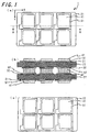
- a laminated heat dissipating base body 1 of the embodiment comprises: a first base 21 and a second base 22 having insulation properties arranged one above the other to face each other; a heat dissipating member 42 sandwiched between the first base 21 and the second base 22; and circuit members 41 disposed on a top surface of the first base 21 arranged above the second base 22 and a bottom surface of the second base 22 arranged below the first base 21, respectively.
- a bonding member is interposed in at least either between the first base 21 (the second base 22 as well) and the heat dissipating member 42 or between the first base 21 (the second base 22 as well) and the circuit member 41 (in the construction shown in Fig.
- the bonding member is interposed both between the first base 21 (the second base 22 as well) and the heat dissipating member 42 and between the first base 21 (the second base 22 as well) and the circuit member 41).
- the first base 21 and the second base 22 are each made of ceramics containing silicon nitride as a major constituent.
- the heat dissipating member 42 is made of a material containing copper as a major constituent.
- the circuit member 41 is made of a material containing copper as a major constituent.
- the bonding member includes a first active metal layer 31 (a second active metal layer 32 as well), and a first bonding layer 51 (a second bonding layer 52 as well) made of a metal containing copper as a major constituent.
- the first and second bonding layers 51 and 52 are each, as will hereinafter be described, made of a metal containing copper as a major constituent (Cu content is 70% by mass or above).
- a metal containing copper as a major constituent Cu content is 70% by mass or above.
- aluminum, an aluminum alloy, an alloy composed predominantly of Mo or W such as a Cu-Mo alloy (Cu content is 15% by mass or above) or a Cu-W alloy (Cu content is 11% by mass or above), and brass (Cu content is 57% by mass or above) may be adopted for use.
- the circuit member 41 while preferably being made of a material composed predominantly of copper as will hereinafter be described, may be made of aluminum or an aluminum alloy
- the heat dissipating member 42 while preferably being made of a material composed predominantly of copper as will hereinafter be described, may be made of any of a metal such as Cu-Mo, Cu-W, aluminum, and an aluminum alloy, Al-SiC (metal-ceramic impregnated material), sintered Cu-diamond, and the like.
- Such a laminated heat dissipating base body 1 can be applied in the speeding up of dissipation of heat from electronic components including a semiconductor element such as an insulated gate bipolar transistor (IGBT) and a metal oxide semiconductor field-effect transistor (MOSFET), a dye-sublimation thermal printer head element, and a thermal ink-jet printer head element.
- a semiconductor element such as an insulated gate bipolar transistor (IGBT) and a metal oxide semiconductor field-effect transistor (MOSFET)
- IGBT insulated gate bipolar transistor
- MOSFET metal oxide semiconductor field-effect transistor
- the first and second bases 21 and 22 constituting the laminated heat dissipating base body 1 are each made of sintered silicon nitride or a silicon nitride single crystal. Silicon nitride exhibits a thermal conductivity as high as 40 W/(m ⁇ K) or above and is excellent in heat dissipation characteristics.
- Each of the first and second bases 21 and 22 ranges from 30 to 80 mm in length in an X direction indicated in Fig. 1 , and ranges from 10 to 80 mm in length in a Y direction indicated in Fig. 1 . Moreover, it is advisable that the thickness of each base ranges from 0.13 to 0.4 mm from the viewpoint of low thermal resistance and high durability.
- the silicon nitride content in each of the first and second bases 21 and 22 is at least 80% by mass or above.
- erbium oxide, magnesium oxide, silicon oxide, molybdenum oxide, aluminum oxide, and the like may be contained therein.
- aluminum oxide alone as an additive component, and the content thereof is preferably set at or below 0.3% by mass.
- the first and second bases 21 and 22 have the following mechanical characteristics: a three-point bending strength of 700 MPa or above; Young's modulus of 300 GPa or above; a Vickers hardness (Hv) of 13 GPa or above; and also a fracture toughness (K 1C ) of preferably 5 MPam 1/2 or above.
- This allows the resulting laminated heat dissipating base body 1 to give a long-term service.
- a higher degree of reliability, and more particularly improved creep resistance and heat cycle durability can be ensured so long as the mechanical characteristics take on the values falling in the aforementioned ranges.
- the first active metal layer 31, the second active metal layer 32, the first bonding layer 51, the second bonding layer 52, the circuit member 41, and the heat dissipating member 42 are removed from the laminated heat dissipating base body 1 by means of etching. After that, measurement is conducted in conformity with JIS R 1601-1995. However, in a case where the thickness of the first base 21 (the second base 22 as well) is so small that it is impossible to set the thickness of a test piece cut from the first base 21 (the second base 22 as well) at 3 mm, the thickness of the first base 21 (the second base 22 as well) in itself is deemed as the thickness of the test piece for evaluation.
- the result of measurement shall fulfill the aforementioned three-point bending strength value.
- the Young's modulus is concerned, at first, the first active metal layer 31, the second active metal layer 32, the first bonding layer 51, the second bonding layer 52, the circuit member 41, and the heat dissipating member 42 are removed from the laminated heat dissipating base body 1 by means of etching. After that, measurement is conducted in accordance with the Indentation Fracture method (IF method) defined by JIS R 1602-1995.
- IF method Indentation Fracture method
- the thickness of the first base 21 (the second base 22 as well) is so small that it is impossible to set the thickness of a test piece cut from the first base 21 (the second base 22 as well) at 4 mem
- the thickness of the first base 21 (the second base 22 as well) in itself is deemed as the thickness of the test piece for evaluation.
- the result of measurement shall fulfill the aforementioned Young's modulus value.
- the Vickers hardness (Hv) and the fracture toughness (K 1C ) are measured in conformity with JIS R 1610-2003 and JIS R 1607-1995, respectively.
- the volume resistivity of the base is greater than or equal to 10 14 ⁇ cm at room temperatures, and is greater than or equal to 10 12 ⁇ cm at 300°C. This makes it possible to prevent leakage of electric current from the circuit member side to the heat dissipating member side during the operation of the laminated heat dissipating base body 1, and thereby lessen the degree of power loss. It is also possible to decrease the possibility that the electronic device fails to work properly.
- the first active metal layer 31 and the second active metal layer 32 formed on the respective main surfaces of the first base 21 (the second base 22 as well) are each made for example of an active metal such as titanium (Ti), zirconium (Zr), and hafnium (Hf), or may occasionally be made of a tin (Sn)-containing Ag-Cu alloy or Au-Cu alloy.
- an active metal such as titanium (Ti), zirconium (Zr), and hafnium (Hf)
- tin (Sn)-containing Ag-Cu alloy or Au-Cu alloy are each and every first active metal layer 31 ranges in length in the X direction from 12.4 to 24.4 mm, ranges in length in the Y direction from 16.4 to 20.4 mm, and ranges in thickness from 10 to 20 ⁇ m.
- each and every second active metal layer 32 ranges in length in the X direction from 12.4 to 22.4 mm, ranges in length in the Y direction from 16.4 to 24.4 mm, and ranges in thickness from 10 to 20 ⁇ m.
- the first bonding layer 51 and the second bonding layer 52 interposed between the first active metal layer 31 and the circuit member 41 and between the second active metal layer 32 and the heat dissipating member 42, respectively, are each composed predominantly of copper.
- the circuit member 41 and the heat dissipating member 42 can be bonded firmly to their respective main surfaces at a temperature as low as 300 to 500°C.
- the bonding can be achieved under a small load. Further, a thermal stress induced during cooling can be relieved by the deformation of the first and second bonding layers 51 and 52.
- first and second bonding layers 51 and 52 are each composed predominantly of copper. Optimally each of the first and second bonding layers 51 and 52 should contain copper as a major constituent in an amount of greater than or equal to 99.96% by mass.
- a copper material such as oxygen-free copper, tough pitch copper, and phosphorus deoxidized copper, capable of achieving firm bonding between the first active metal layer 31 and the circuit member 41 and between the second active metal layer 32 and the heat dissipating member 42.
- any of linear crystal oxygen-free copper, single crystal high-purity oxygen-free copper, and vacuum melted copper that have a copper content of greater than or equal to 99. 995% by mass.
- the higher is the copper content the lower is the electrical resistance and the higher is the heat conductivity. Accordingly, excellent circuit characteristics (special property of being able to prevent heat generation in electronic components and thus reduce power loss) and excellent heat dissipation characteristics can be attained.
- the higher is the copper content the lower is the yield stress and the more likely it is that there arises plastic deformation at high temperatures. Accordingly, the strength of bonding between the first bonding layer 51 and the circuit member 41 and between the second bonding layer 52 and the heat dissipating member 42 can be increased with consequent enhancement in reliability,
- the bonding member is interposed both between the first base 21 (the second base 22 as well) and the heat dissipating member 42 and between the first base 21 (the second base 22 as well) and the circuit member 41.
- an intermediate layer may be inserted between the first active metal layer 31 and the first bonding layer 51 or between the second active metal layer 32 and the second bonding layer 52.
- the intermediate layer should preferably be made of a material which is readily deformable elastically or plastically.
- the intermediate layer is made of Al, Ni, an alloy containing such a metal, or such a metal-based foam metal or metallic wire bundle.
- the intermediate layer should preferably contain a component which is smaller than copper but larger than silicon nitride in thermal expansion coefficient, for example, at least one of W, Mo, Ti, Cu-Mo, Cu-W, and WC-Co.
- the length thereof in the X direction is so selected as to fall in a range of from 10 to 17 mm
- the length thereof in the Y direction is so selected as to fall in a range of from 10 to 20 mm
- the thickness thereof is so selected as to fall in a range of from 0.5 to 5 mm in accordance with the magnitude of electric current passing through the circuit and the amount of heat produced in an electronic component such as a semiconductor element mounted on the circuit member 41.
- the heat dissipating member 42 has the function of dissipating heat liberated by the electronic component in a heat-producing state.
- Each and every heat dissipating member 42 ranges in length in the X direction from 10 to 17 mm, ranges in length in the Y direction from 10 to 20 mm, and ranges in thickness from 0.5 to 5 mm.
- the circuit member 41 and the heat dissipating member 42 are each composed predominantly of copper or a copper alloy.
- the copper or copper alloy should preferably constitute 90% or above of each of the circuit member 41 and the heat dissipating member 42 by mass.
- a copper material such as oxygen-free copper, tough pitch copper, and phosphorus deoxidized copper.
- oxygen-free copper materials any of linear crystal oxygen-free copper, single crystal high-purity oxygen-free copper, and vacuum melted copper that have a copper content of greater than or equal to 99. 995% by mass is particularly desirable for use.
- the circuit members 41 are arranged in the form of a matrix with a plurality of rows and a plurality of columns. By arranging the circuit members 41 in matrix form, it is possible to design the first base 21 (the second base 22 as well) in the shape of a square or a nearly-square rectangle, and thereby suppress warpage occurring in the laminated heat dissipating base body 1.
- the heat dissipating members 42 are also arranged in the form of a matrix with a plurality of rows and a plurality of columns.
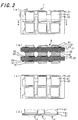
- the first bonding layer 51 consists of irregular parts that are continuous with each other so as to extend over the circuit members 41.
- the first bonding layer 51 serves as a wiring line for establishing connection between the circuit members 41, it is possible to eliminate the need to install wire interconnection.
- great current can be passed through the electronic component such as a semiconductor element.
- the first bonding layer 51 consists of irregular parts that are continuous with each other so as to extend over the circuit members 41.
- the difference between the laminated heat dissipating base body 1 shown in Fig. 3 and that shown in Fig. 2 is that the thickness of the first bonding layer 51 varies from part to part, and more specifically, as compared with a region of the first bonding layer on which is placed the circuit member 41, which is termed "the circuit member placement region E", a region thereof located between the adjacent circuit members 41, which is termed “the inter-circuit member region F", is made smaller in thickness.
- Fig. 8(a) is a diagram schematically showing warpage occurring in a first base 21a constituting a laminated heat dissipating base body 1a of the present embodiment in which the circuit members are arranged in an array of one row and a plurality of columns, or arranged in an array of a plurality of rows and one column on the top surface of the first base 21a.
- Fig. 8(a) is a diagram schematically showing warpage occurring in a first base 21a constituting a laminated heat dissipating base body 1a of the present embodiment in which the circuit members are arranged in an array of one row and a plurality of columns, or arranged in an array of a plurality of rows and one column on the top surface of the first base 21a.
- FIG. 8(b) is a diagram schematically showing warpage occurring in a first base 21b constituting a laminated heat dissipating base body 1b of the present embodiment in which the circuit members are arranged in an array of one row and a plurality of columns, or arranged in an array of a plurality of rows and one column on the top surface of the first base 21b.
- the first base 21a can be made shorter in longitudinal length.
- a warpage (H 1 ) occurring in the first base 21a of the laminated heat dissipating base body 1a of the present embodiment can be smaller than a warpage (H 2 ) occurring in the first base 21b of the laminated heat dissipating base body 1b.
- the thickness of the heat dissipating member 42 is 1 to 10 times that of the circuit member 41.
- the laminated heat dissipating base body 1 can be made compact, wherefore the heat liberated by the electronic component can be diffused thoroughly; a member having a forced cooling capability can be incorporated into the heat dissipating member 42, wherefore efficient heat dissipation can be achieved; and the heat dissipating member 42 can be made sufficiently thick with consequent increase in the rigidity of the laminated heat dissipating base body 1, and thus, even if the laminated heat dissipating base body 1 is subjected to thermal hysteresis, by virtue of deformation constraint effect, warpage can be suppressed with consequent increase in reliability.
- the heat diffusivity of the heat dissipating member 42 and the reliability of the laminated heat dissipating base body 1 vary depending on the position of an end face of the heat dissipating member 42 in a planar view in a see-through manner from above (as viewed in the thicknesswise direction). It is preferable that the end face of the heat dissipating member 42 in a planar view in a see-through manner (as viewed in the thicknesswise direction) is located outwardly from an end face of the circuit member 41. By doing so, the heat diffused in the circuit member 41 can be further diffused in the heat dissipating member 42. This helps enhance the heat dissipation characteristics even further.
- the end face of the heat dissipating member 42 in a planar view in a see-through manner from above (as viewed in the thicknesswise direction) is spaced 0.1 to 2 mm outwardly from the end face of the circuit member 41.
- the end face of the heat dissipating member 42 in a planar view in a see-through manner from above (as viewed in the thicknesswise direction) is located inwardly from an end face of the first base 21 or the second base 22.
- the end face of the heat dissipating member 42 in a planar view in a see-through manner from above (as viewed in the thicknesswise direction) is spaced 0.1 to 5 mm inwardly from the end face of the first base 21 or the second base 22.
- each of the circuit member 41 and the heat dissipating member 42 ranges in Vickers hardness (Hv) from 0.5 to 1.2 GPa.
- the volume of each of the circuit member 41 and the heat dissipating member 42 can be measured by means of a three-dimensional shape measuring instrument, or can also be measured by means of a metallographic microscope, an image measuring instrument, or otherwise at a magnification of 2 to 10 times. It is advisable that the Vickers hardness (Hv) of each of the circuit member 41 and the heat dissipating member 42 is measured in conformity with JIS Z 2244-2003. A test load adopted for measurement is dependent on the thickness of each of the circuit member 41 and the heat dissipating member 42. For example, the test load is set at 196 mN (millinewton).
- the circuit members 41 and the heat dissipating members 42 which are bonded to their respective main surfaces of the first base 21 (the second base 22 as well), are arranged in the form of a matrix with three rows and three columns.
- This laminated heat dissipating base body 1 is one of examples in which the circuit members 41 and the heat dissipating members 42 to be bonded to their respective base main surfaces are arranged in the form of a matrix with an odd number of plural rows and an odd number of plural columns.
- a heat dissipating member 41c and a circuit member 42c lie on a point of intersection of two diagonal lines each connecting the opposite corners of the square-shaped first base 21 (the square-shaped second base 22 as well), wherefore the deformation of the laminated heat dissipating base body 1 occurring during the step of bonding the heat dissipating member 41c and the circuit member 42c is constrained. This makes it possible to suppress warpage occurring in the laminated heat dissipating base body 1 successfully.
- the heat dissipating member 42 is formed with a hollow 42a.
- the hollow 42a is a columnar space.
- the heat dissipating member 42 having the hollow 42a has a larger surface area as a whole, wherefore the heat dissipation characteristics can be enhanced even further.
- a member having a forced cooling capability can be set in the hollow. This makes it possible to dissipate the heat liberated by the electronic component more efficiently.
- the proportion of the hollow 42a to the entire heat dissipating member 42 falls in a range of 20% by volume or more and 80% by volume or less. By doing so, the risk of buckling distortion and buckling fracture can be reduced in the bonding step, and also the surface area of the hollow 42a can be increased. This leads to further enhancement in the heat dissipation characteristics.
- the hardness of the first bonding layer S1 affects the strength of bonding between it and the circuit member 41
- the hardness of the second bonding layer 52 affects the strength of bonding between it and the heat dissipating member 42.
- the Vickers hardness (Hv) of each of the bonding layers 51 and 52 is preferably set at or below 0.5 GPa. By setting the Vickers hardness (Hv) in that way, the bonding layers 51 and 52 are readily deformable with consequent increase in the strength of bonding between the bonding layer and the circuit member 41 as well as the heat dissipating member 42. It is particularly desirable to set the Vickers hardness (Hv) in a range of from 0.2 to 0.5 GPa.
- the Vickers hardness (Hv) of each of the first and second bonding layers 51 and 52 is measured in conformity with JIS Z 2244-2003.
- a test load adopted for measurement is dependent on the thickness of each of the first and second bonding layers 51 and 52.
- the test load is set at 98 mN or 196 mN.
- a heat dissipating unit 61 having a frame body 62 disposed in contact with the top surface of the first base 21, the bottom surface of the second base 22, the side surfaces of the first base 21, and the side surfaces of the second base 22, for surrounding the laminated heat dissipating base body 1.
- the frame body 62 is made of one or more of materials including copper, a copper alloy, aluminum, an aluminum alloy, and resin.
- a cooling medium such as water, coolant water, oil, liquid nitrogen, or liquid argon is introduced into the frame body 62 through a pipe-shaped inlet 63 inserted into the frame body 62.
- the inlet 63 is made of the aforementioned metal material or resin.
- the cooling medium that was used for cooling is discharged through a pipe-shaped outlet 64 disposed in the frame body 62.
- the outlet 64 made of the aforementioned metal material or resin.
- the frame body 62 is disposed in contact with the top surface of the first base 21, the bottom surface of the second base 22, the side surfaces of the first base 21, and the side surfaces of the second base 22, the frame body 62 may be so di.sposed as to make contact with at least one of the top surface of the first base 21 and the bottom surface of the second base 22.
- a cooling pipe 65 such as a heat pipe is inserted in the hollow 42a.
- the cooling pipe 65 is made of any of copper, a copper alloy, aluminum, and an aluminum alloy.
- Cooling means 66 such as a radiator is connected to the cooling pipe 65.
- the laminated heat dissipating base body can be cooled down efficiently and inexpensively without the necessity of providing a large-sized cooling device.
- the electronic device of the invention is free from accumulation of heat in the electronic components during operation and hence succeeds in offering high heat dissipation capability.
- the laminated heat dissipating base body 1 of the invention is constructed as follows. At first, a paste of a Ag-Cu alloy or Au-Cu alloy, which contains an active metal such as titanium (Ti), zirconium (Zr), hafnium (Hf), etc. and may occasionally contain tin (Sn), is applied onto both of the main surfaces of the first base 21 (the second base 22 as well) made of sintered silicon nitride that ranges in length from 30 to 80 mm, ranges in width from 10 to 80 mm, and ranges in thickness from 0.13 to 0.4 mm by means of screen printing, roll coater technique, brush coating, or otherwise.
- an active metal such as titanium (Ti), zirconium (Zr), hafnium (Hf), etc. and may occasionally contain tin (Sn)
- the laminated body is caused to melt under application of heat at a temperature of 800 to 900°C.
- the first and second active metal layers 31 and 32 and the first and second bonding layers 51 and 52 composed predominantly of copper are formed.
- the laminated heat dissipating base body 1 is obtained.
- the laminated heat dissipating base body 1 is then cooled down to a temperature at which neither copper nor copper alloy will be oxidized (50°C) under application of pressure. Upon this temperature being reached, the pressurization is brought to an end and the laminated heat dissipating base body 1 is taken out.
- the formation of the circuit in the circuit member 41 is concerned, specifically, it is possible to use a copper plate having a circuit formed therein in advance by patterning using press working or etching technique. It is also possible to form a circuit by patterning using etching, laser processing, or the like technique following the completion of bonding of the circuit member.
- the first bonding layer 51 formed in accordance with the aforestated method is subjected to etching, laser processing, or the like operation, with the areas thereof other than the inter-circuit member region F kept masked, so that that part of the first bonding layer 51 which corresponds to the inter-circuit member region F can be processed into a thin region. After that, the masking material is removed, whereupon the laminated heat dissipating base body 1 can be obtained.
- the laminated heat dissipating base body 1 in which the circuit member 41 and the heat dissipating member 42 have a large thickness is able to offer enhanced heat dissipation characteristics and may occasionally be in no need of attachment of a heat sink.
- the electronic component such as a semiconductor element is connected to the circuit member of the laminated heat dissipating base body 1, even during the use of the electronic device such as a semiconductor apparatus, it is possible to effectively prevent accumulation of heat in the electronic component.
- the laminated heat dissipating base body 1 of the invention is excellent in heat dissipation characteristics as heretofore described and is therefore applicable to a substrate for use in a dye-sublimation thermal printer head, a planar heat-generating heater support substrate, a heater support substrate for use in a thermal ink-jet printer head, and so forth.
Landscapes
- Chemical & Material Sciences (AREA)
- Engineering & Computer Science (AREA)
- Ceramic Engineering (AREA)
- Materials Engineering (AREA)
- Structural Engineering (AREA)
- Organic Chemistry (AREA)
- Microelectronics & Electronic Packaging (AREA)
- Cooling Or The Like Of Semiconductors Or Solid State Devices (AREA)
- Structure Of Printed Boards (AREA)
Applications Claiming Priority (2)
| Application Number | Priority Date | Filing Date | Title |
|---|---|---|---|
| JP2007143956 | 2007-05-30 | ||
| PCT/JP2008/060068 WO2008149818A1 (fr) | 2007-05-30 | 2008-05-30 | Corps de base dissipateur de chaleur stratifié, et unité dissipatrice de chaleur et dispositif électronique utilisant le corps de base dissipateur de chaleur stratifié |
Publications (2)
| Publication Number | Publication Date |
|---|---|
| EP2157607A1 true EP2157607A1 (fr) | 2010-02-24 |
| EP2157607A4 EP2157607A4 (fr) | 2012-09-05 |
Family
ID=40093636
Family Applications (1)
| Application Number | Title | Priority Date | Filing Date |
|---|---|---|---|
| EP08777066A Withdrawn EP2157607A4 (fr) | 2007-05-30 | 2008-05-30 | Corps de base dissipateur de chaleur stratifié, et unité dissipatrice de chaleur et dispositif électronique utilisant le corps de base dissipateur de chaleur stratifié |
Country Status (3)
| Country | Link |
|---|---|
| EP (1) | EP2157607A4 (fr) |
| JP (1) | JP5144657B2 (fr) |
| WO (1) | WO2008149818A1 (fr) |
Cited By (3)
| Publication number | Priority date | Publication date | Assignee | Title |
|---|---|---|---|---|
| EP2579696A4 (fr) * | 2010-05-27 | 2017-11-08 | Kyocera Corporation | Carte de circuit imprimé et dispositif électronique doté d'une telle carte |
| EP3252810A4 (fr) * | 2015-01-29 | 2018-10-10 | Kyocera Corporation | Carte de circuit imprimé et dispositif électronique |
| WO2025073566A1 (fr) * | 2023-10-02 | 2025-04-10 | Brusa Elektronik Ag | Élément de connexion entre un composant électrique émetteur de chaleur et un dissipateur thermique, et carte de circuit électrique comprenant un tel élément de connexion |
Families Citing this family (5)
| Publication number | Priority date | Publication date | Assignee | Title |
|---|---|---|---|---|
| JP6392583B2 (ja) * | 2014-08-25 | 2018-09-19 | 京セラ株式会社 | 回路基板、および電子装置 |
| JP6471465B2 (ja) * | 2014-11-11 | 2019-02-20 | 三菱マテリアル株式会社 | 冷却器付パワーモジュール用基板 |
| DE102019126954B4 (de) * | 2019-10-08 | 2024-12-05 | Rogers Germany Gmbh | Verfahren zur Herstellung eines Metall-Keramik-Substrats, Lötsystem und Metall-Keramik-Substrat, hergestellt mit einem solchen Verfahren |
| DE102019135099A1 (de) * | 2019-12-19 | 2021-06-24 | Rogers Germany Gmbh | Verfahren zur Herstellung eines Metall-Keramik-Substrats und Metall-Keramik-Substrat, hergestellt mit einem solchen Verfahren |
| DE102019135097A1 (de) * | 2019-12-19 | 2021-06-24 | Rogers Germany Gmbh | Verfahren zur Herstellung eines Metall-Keramik-Substrats und Metall-Keramik-Substrat, hergestellt mit einem solchen Verfahren |
Family Cites Families (10)
| Publication number | Priority date | Publication date | Assignee | Title |
|---|---|---|---|---|
| DE3165502D1 (en) * | 1980-04-21 | 1984-09-20 | Bbc Brown Boveri & Cie | Multi-layered-solder and method of producing such solder |
| JPS5957973A (ja) * | 1982-09-25 | 1984-04-03 | 日本特殊陶業株式会社 | 金属・セラミツクス複合体 |
| US4729504A (en) * | 1985-06-01 | 1988-03-08 | Mizuo Edamura | Method of bonding ceramics and metal, or bonding similar ceramics among themselves; or bonding dissimilar ceramics |
| US4740429A (en) * | 1985-07-22 | 1988-04-26 | Ngk Insulators, Ltd. | Metal-ceramic joined articles |
| JP2939444B2 (ja) * | 1996-09-18 | 1999-08-25 | 株式会社東芝 | 多層窒化けい素回路基板 |
| JPH09191059A (ja) * | 1996-12-04 | 1997-07-22 | Denki Kagaku Kogyo Kk | パワー半導体モジュール基板 |
| EP0935286A4 (fr) * | 1997-05-26 | 2008-04-09 | Sumitomo Electric Industries | Substrat jonction de circuit en cuivre et procede de production de ce substrat |
| JP2004022973A (ja) * | 2002-06-19 | 2004-01-22 | Kyocera Corp | セラミック回路基板および半導体モジュール |
| JP2006245479A (ja) * | 2005-03-07 | 2006-09-14 | Nichicon Corp | 電子部品冷却装置 |
| JP4595665B2 (ja) * | 2005-05-13 | 2010-12-08 | 富士電機システムズ株式会社 | 配線基板の製造方法 |
-
2008
- 2008-05-30 WO PCT/JP2008/060068 patent/WO2008149818A1/fr not_active Ceased
- 2008-05-30 EP EP08777066A patent/EP2157607A4/fr not_active Withdrawn
- 2008-05-30 JP JP2009517850A patent/JP5144657B2/ja not_active Expired - Fee Related
Cited By (3)
| Publication number | Priority date | Publication date | Assignee | Title |
|---|---|---|---|---|
| EP2579696A4 (fr) * | 2010-05-27 | 2017-11-08 | Kyocera Corporation | Carte de circuit imprimé et dispositif électronique doté d'une telle carte |
| EP3252810A4 (fr) * | 2015-01-29 | 2018-10-10 | Kyocera Corporation | Carte de circuit imprimé et dispositif électronique |
| WO2025073566A1 (fr) * | 2023-10-02 | 2025-04-10 | Brusa Elektronik Ag | Élément de connexion entre un composant électrique émetteur de chaleur et un dissipateur thermique, et carte de circuit électrique comprenant un tel élément de connexion |
Also Published As
| Publication number | Publication date |
|---|---|
| JP5144657B2 (ja) | 2013-02-13 |
| EP2157607A4 (fr) | 2012-09-05 |
| WO2008149818A1 (fr) | 2008-12-11 |
| JPWO2008149818A1 (ja) | 2010-08-26 |
Similar Documents
| Publication | Publication Date | Title |
|---|---|---|
| EP2109138B1 (fr) | Substrat de dissipation de chaleur et dispositif electronique utilisant un tel substrat | |
| EP2157607A1 (fr) | Corps de base dissipateur de chaleur stratifié, et unité dissipatrice de chaleur et dispositif électronique utilisant le corps de base dissipateur de chaleur stratifié | |
| EP2259308B1 (fr) | Substrat pour module de puissance a dissipateur thermique et son procede de fabrication, module de puissance a dissipateur thermique, et substrat pour module de puissance | |
| EP2372758A2 (fr) | Dispositif de refroidissement | |
| EP2012355A2 (fr) | Plaque de dissipation thermique et dispositif semiconducteur | |
| US20100302734A1 (en) | Heatsink and method of fabricating same | |
| CN103227154A (zh) | 具有压印底板的功率半导体模块及其制造方法 | |
| JP5370460B2 (ja) | 半導体モジュール | |
| JP2004022973A (ja) | セラミック回路基板および半導体モジュール | |
| JP2005011922A (ja) | ヒートシンクを備えた両面銅貼り基板、およびこれを用いた半導体装置 | |
| JP4744385B2 (ja) | 放熱基板およびこれを用いた電子装置 | |
| JP4893096B2 (ja) | 回路基板およびこれを用いた半導体モジュール | |
| JP4893095B2 (ja) | 回路基板およびこれを用いた半導体モジュール | |
| JP2009088176A (ja) | 放熱基体およびこれを用いた電子装置 | |
| JP2012191004A (ja) | パワーモジュール用基板の製造方法及びパワーモジュール用基板 | |
| JP6565735B2 (ja) | パワーモジュール用基板及びパワーモジュール並びにパワーモジュール用基板の製造方法 | |
| JP5649489B2 (ja) | 放熱基板およびこれを用いた電子装置 | |
| JPH0799268A (ja) | 半導体用高熱伝導性セラミックスパッケージ | |
| EP3696851B1 (fr) | Agencement de semiconducteur et son procédé de fabrication | |
| JPH10200219A (ja) | 回路基板 | |
| JPH10173109A (ja) | パワー半導体モジュール | |
| EP4444674B1 (fr) | Substrats intégrés et procédés associés | |
| JPH0851169A (ja) | 半導体装置 | |
| JP2003124584A (ja) | セラミック回路基板 | |
| JP2005277382A (ja) | 電子部品収納用パッケージおよび電子装置 |
Legal Events
| Date | Code | Title | Description |
|---|---|---|---|
| PUAI | Public reference made under article 153(3) epc to a published international application that has entered the european phase |
Free format text: ORIGINAL CODE: 0009012 |
|
| 17P | Request for examination filed |
Effective date: 20091230 |
|
| AK | Designated contracting states |
Kind code of ref document: A1 Designated state(s): AT BE BG CH CY CZ DE DK EE ES FI FR GB GR HR HU IE IS IT LI LT LU LV MC MT NL NO PL PT RO SE SI SK TR |
|
| AX | Request for extension of the european patent |
Extension state: AL BA MK RS |
|
| DAX | Request for extension of the european patent (deleted) | ||
| A4 | Supplementary search report drawn up and despatched |
Effective date: 20120807 |
|
| RIC1 | Information provided on ipc code assigned before grant |
Ipc: H01L 23/373 20060101ALI20120731BHEP Ipc: H05K 1/02 20060101ALI20120731BHEP Ipc: H01L 23/12 20060101ALI20120731BHEP Ipc: H01L 23/36 20060101AFI20120731BHEP Ipc: C04B 37/02 20060101ALI20120731BHEP |
|
| STAA | Information on the status of an ep patent application or granted ep patent |
Free format text: STATUS: THE APPLICATION HAS BEEN WITHDRAWN |
|
| 18W | Application withdrawn |
Effective date: 20130926 |