EP2157659A1 - Mehrband-Monopolschlitzantenne - Google Patents
Mehrband-Monopolschlitzantenne Download PDFInfo
- Publication number
- EP2157659A1 EP2157659A1 EP08170263A EP08170263A EP2157659A1 EP 2157659 A1 EP2157659 A1 EP 2157659A1 EP 08170263 A EP08170263 A EP 08170263A EP 08170263 A EP08170263 A EP 08170263A EP 2157659 A1 EP2157659 A1 EP 2157659A1
- Authority
- EP
- European Patent Office
- Prior art keywords
- monopole slot
- antenna
- monopole
- multiband
- metal surface
- Prior art date
- Legal status (The legal status is an assumption and is not a legal conclusion. Google has not performed a legal analysis and makes no representation as to the accuracy of the status listed.)
- Granted
Links
Images

Classifications
-
- H—ELECTRICITY
- H01—ELECTRIC ELEMENTS
- H01Q—ANTENNAS, i.e. RADIO AERIALS
- H01Q1/00—Details of, or arrangements associated with, antennas
- H01Q1/12—Supports; Mounting means
- H01Q1/22—Supports; Mounting means by structural association with other equipment or articles
- H01Q1/24—Supports; Mounting means by structural association with other equipment or articles with receiving set
- H01Q1/241—Supports; Mounting means by structural association with other equipment or articles with receiving set used in mobile communications, e.g. GSM
- H01Q1/242—Supports; Mounting means by structural association with other equipment or articles with receiving set used in mobile communications, e.g. GSM specially adapted for hand-held use
- H01Q1/243—Supports; Mounting means by structural association with other equipment or articles with receiving set used in mobile communications, e.g. GSM specially adapted for hand-held use with built-in antennas
-
- H—ELECTRICITY
- H01—ELECTRIC ELEMENTS
- H01Q—ANTENNAS, i.e. RADIO AERIALS
- H01Q13/00—Waveguide horns or mouths; Slot antennas; Leaky-waveguide antennas; Equivalent structures causing radiation along the transmission path of a guided wave
- H01Q13/10—Resonant slot antennas
- H01Q13/106—Microstrip slot antennas
-
- H—ELECTRICITY
- H01—ELECTRIC ELEMENTS
- H01Q—ANTENNAS, i.e. RADIO AERIALS
- H01Q21/00—Antenna arrays or systems
- H01Q21/30—Combinations of separate antenna units operating in different wavebands and connected to a common feeder system
-
- H—ELECTRICITY
- H01—ELECTRIC ELEMENTS
- H01Q—ANTENNAS, i.e. RADIO AERIALS
- H01Q5/00—Arrangements for simultaneous operation of antennas on two or more different wavebands, e.g. dual-band or multi-band arrangements
- H01Q5/40—Imbricated or interleaved structures; Combined or electromagnetically coupled arrangements, e.g. comprising two or more non-connected fed radiating elements
Definitions
- the present invention relates to a slot antenna, and more particularly, to a multiband monopole slot antenna suitable for application in mobile communication devices.
- Taiwan patent No. 1293215 entitled “Dual-Band Inverted-F Antenna”
- a ground plane built in the backplane of the LCD display of a notebook computer and a dual-band antenna designed thereon are disclosed.
- the antenna is only suitable for WLAN operation due to its size; it is difficult to fit into a mobile communication device when it is applied as a multiband antenna used in the mobile communication system.
- the antenna disclosed in the present invention comprises: a ground plane, a dielectric substrate, a radiating portion and a microstrip feedline.
- the dielectric substrate is connected to an edge of the ground plane and extends toward the opposite direction of the ground plane.
- the dielectric substrate has a metal surface, which can be formed on the dielectric substrate by printing or etching and the metal surface is electrically connected to the ground plane via at least one electrical connecting point.
- the radiating portion is on the metal surface of the dielectric substrate and comprises at least a first monopole slot, a second monopole slot, and a third monopole slot, wherein the first, the second, and the third monopole slots each have an open end and a terminal, the open end is on a side edge of the metal surface, and the terminal is extended inward the metal surface.
- the second monopole slot is substantially parallel to the first monopole slot; the third monopole slot is positioned between the first monopole slot and the second monopole slot.
- the microstrip feedline is on the surface opposite to the metal surface of the dielectric substrate and can be printed or etched on the dielectric substrate.
- a first end of the microstrip feedline is connected to a signal source, and a second end of the microstrip feedline is an open end.
- the microstrip feedline passes over the first, second, and third monopole slots.
- a section of the microstrip feedline which passes over the third monopole slot is substantially parallel to the third monopole slot, and the microstrip feedline is generally of a step shape.
- the antenna disclosed in the present invention is designed as a multiband monopole slot antenna, which can be operated in communication bands such as GSM850 (824 ⁇ 894 MHz), GSM900 (890 - 960 MHz), and DCS/PCS/UMTS (1710 - 1880 MHz/1850 ⁇ 1990 MHz/1920 ⁇ 2170 MHz).
- the multiband monopole slot antenna is series-fed by the microstrip feedline in different positions of the three monopole slots, wherein the microstrip feedline is generally of a step shape and comprises a section parallel to one of the three monopole slots for controlling the feeding position of the monopole slots so as to generate a resonant mode in the lower-frequency band, thereby enabling multiband operation covering the GSM850/900 and DCS/PCS/UMTS bands.
- the first monopole slot can generate a resonant mode near a quarter wavelength of a lower frequency at about 900 MHz
- the second monopole slot can generate a resonant mode near a quarter wavelength of a higher frequency at about 1900 MHz
- the third monopole slot can also generate a resonant mode near a quarter wavelength of the lower frequency at about 900 MHz to form a lower-frequency band with the resonant mode generated by the first monopole slot; in addition, the resonant mode generated by the second monopole slot can form a higher-frequency band.
- the central frequencies of the lower-frequency band and the higher-frequency band can be adjusted by changing the feeding positions of the microstrip feedline corresponding to the first and the second monopole slots. Furthermore, a section of the microstrip feedline parallel to the third monopole slot can also effectively adjust the resonant mode of the third monopole slot to provide good impedance matching; therefore, the present invention can enable multiband operation covering the GSM850/900 and DCS/PCS/UMTS bands.
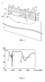
- FIG. 1 illustrates a structural view of a multiband antenna in a first embodiment of the present invention.
- the multiband antenna 1 comprises a ground plane 10, a dielectric substrate 11, a radiating portion 12, and a microstrip feedline 16.
- the ground plane 10 is a metal backplane of an LCD display of a notebook computer.
- the dielectric substrate 11 is at an edge 101 of the ground plane and extends toward the opposite direction of the ground plane 10.
- the dielectric substrate 11 also comprises a metal surface 111, which is electrically connected to the ground plane 10 via at least one electrical connecting point 113.
- the radiating portion 12 on the metal surface 111 of the dielectric substrate 11 comprises at least a first monopole slot 13, a second monopole slot 14, and a third monopole slot 15.
- the first monopole slot 13 comprises an open end 131 and a terminal 132.
- the open end 131 is on a side edge 112 of the metal surface 111, and the terminal 132 extends inward the metal surface 111.
- the second monopole slot 14 is substantially parallel to the first monopole slot 13 and comprises an open end 141 and a terminal 142.
- the open end 141 is on the side edge 112 of the metal surface 111, and the terminal 142 extends inward the metal surface 111.
- the third monopole slot 15 is positioned between the first monopole slot 13 and the second monopole slot 14 and comprises an open end 151 and a terminal 152.
- the open end 151 is on the side edge 112 of the metal surface 111, and the terminal 152 extends inward the metal surface 111.
- the microstrip feedline 16 is generally of a step shape and is on the surface opposite to the metal surface 111 of the dielectric substrate 11. A first end of the microstrip feedline 16 is connected to a signal source 17, and a second end of the microstrip feedline 16 is an open end 161. The microstrip feedline 16 passes over the first monopole slot 13, the second monopole slot 14, and third monopole slot 15. A section 162 of the microstrip feedline 16 which passes over the third monopole slot 15 is substantially parallel to the third monopole slot 15.
- the ground plane 10 being a metal backplane of an LCD display of a notebook computer, is designed to have a length of 260 mm and a width of 200 mm;
- the first monopole slot 13 of the radiating portion 12 has a length of 55 mm (about a quarter wavelength at 900 MHz);
- the second monopole slot 14 has a length of 30 mm (about a quarter wavelength at 1900 MHz);
- the third monopole slot 15 has a length of 58 mm (about a quarter wavelength at 900 MHz).
- the radiating portion 12 is printed or etched on the dielectric substrate 11, which is 60 mm long, 10 mm wide, and 0.8 mm thick.
- FIG. 2 shows a measurement of the return loss of the first embodiment of the present invention.
- the first monopole slot 13 and the third monopole slot 15 can respectively generate a quarter-wavelength resonant mode to jointly form a lower-frequency band 21 of the multiband antenna 1, and the second monopole slot 14 can generate a quarter-wavelength resonant mode to form a higher-frequency band 22.
- the operating bandwidth of the lower-frequency band is about 200 MHz (785 - 985 MHz), which covers the GSM850 (824 - 894 MHz) and the GSM900 (890 ⁇ 960 MHz) bands;
- the operating bandwidth of the higher-frequency band is about 670 MHz (1630 - 2300 MHz), which covers the DCS (1710 - 1880 MHz), PCS (1850 - 1990 MHz), and UMTS (1920 ⁇ 2170 MHz) bands.
- FIG. 3 and FIG. 4 respectively show the gain and the radiation efficiency of the first embodiment of the present invention in a lower-frequency band 21 and a higher-frequency band 22.
- the antenna gain 31 in the lower-frequency band 21 ranges from 0.1 dBi to 0.8 dBi, and the radiation efficiency 32 ranges from 55% to 70%;
- the antenna gain 41 in the higher-frequency band 22 ranges from 0.4 dBi to 2.5 dBi, and the radiation efficiency 42 ranges from 82% to 94%. Therefore, the radiation characteristics of the multiband antenna 1 are suitable for application in mobile communication devices.
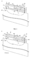
- FIG. 5 illustrates a structural view of the multiband antenna in a second embodiment of the present invention.
- the third monopole slot 55 of the multiband antenna 5 comprises at least two bendings and substantially forms a step shape to keep the terminal 132 of the first monopole slot 13 separated from the terminal 552 of the third monopole slot 55 at a desired distance.
- Other structures of the antenna 5 are the same as those of the antenna 1 of the first embodiment.
- FIG. 6 illustrates a structural view of the multiband antenna in a third embodiment of the present invention.
- the dielectric substrate 61 of the multiband antenna 6 has a bending to allow a portion of the dielectric substrate 61 substantially vertical to the ground plane.
- Other structures of the antenna 6 are the same as those of the antenna 1 of the first embodiment. In this way, the multiband antenna 6 can have various heights and thicknesses to allow placement in different positions in mobile communication devices.
- antennas in the second and the third embodiments can also provide multiband operations as described in the first embodiment.
Landscapes
- Engineering & Computer Science (AREA)
- Computer Networks & Wireless Communication (AREA)
- Physics & Mathematics (AREA)
- Electromagnetism (AREA)
- Waveguide Aerials (AREA)
- Variable-Direction Aerials And Aerial Arrays (AREA)
- Details Of Aerials (AREA)
Applications Claiming Priority (1)
| Application Number | Priority Date | Filing Date | Title |
|---|---|---|---|
| TW097131769A TWI341053B (en) | 2008-08-20 | 2008-08-20 | Multiband monopole slot antenna |
Publications (2)
| Publication Number | Publication Date |
|---|---|
| EP2157659A1 true EP2157659A1 (de) | 2010-02-24 |
| EP2157659B1 EP2157659B1 (de) | 2011-01-12 |
Family
ID=40474966
Family Applications (1)
| Application Number | Title | Priority Date | Filing Date |
|---|---|---|---|
| EP08170263A Active EP2157659B1 (de) | 2008-08-20 | 2008-11-28 | Mehrband-Monopolschlitzantenne |
Country Status (5)
| Country | Link |
|---|---|
| US (1) | US8223083B2 (de) |
| EP (1) | EP2157659B1 (de) |
| AT (1) | ATE495559T1 (de) |
| DE (1) | DE602008004522D1 (de) |
| TW (1) | TWI341053B (de) |
Cited By (4)
| Publication number | Priority date | Publication date | Assignee | Title |
|---|---|---|---|---|
| CN101800361A (zh) * | 2010-03-23 | 2010-08-11 | 中兴通讯股份有限公司 | 一种无线设备 |
| EP2445053A1 (de) * | 2010-10-22 | 2012-04-25 | Acer Incorporated | Mobiles Kommunikationsgerät und Antenne |
| EP2509158A3 (de) * | 2011-04-08 | 2013-04-03 | Acer Incorporated | Elektronisches Kommunikationsgerät und Antennenstruktur dafür |
| CN104241865A (zh) * | 2013-06-11 | 2014-12-24 | 深圳富泰宏精密工业有限公司 | 天线组件 |
Families Citing this family (14)
| Publication number | Priority date | Publication date | Assignee | Title |
|---|---|---|---|---|
| TWI436526B (zh) * | 2010-04-20 | 2014-05-01 | Quanta Comp Inc | Can suppress the maximum gain of the multi-frequency antenna |
| WO2012047085A1 (en) | 2010-10-05 | 2012-04-12 | Laird Technologies, Inc. | Multi-band, wide-band antennas |
| CN102456943B (zh) * | 2010-10-28 | 2014-12-17 | 宏碁股份有限公司 | 移动通讯装置和天线装置 |
| CN102842747B (zh) * | 2011-06-21 | 2014-12-17 | 英华达(上海)科技有限公司 | 具调整槽道的单极槽孔天线结构 |
| TWI619308B (zh) * | 2013-06-10 | 2018-03-21 | 群邁通訊股份有限公司 | 天線組件 |
| KR20140148150A (ko) * | 2013-06-21 | 2014-12-31 | 삼성전자주식회사 | 안테나장치 및 이를 구비한 디스플레이장치 |
| CN104319477B (zh) * | 2014-09-18 | 2018-02-27 | 联想(北京)有限公司 | 一种天线及电子设备 |
| EP3194898A4 (de) | 2014-09-18 | 2017-09-13 | Arad Measuring Technologies Ltd. | Verbrauchszähler mit einem zählerregister mit verwendung einer mehrfachresonanzantenne |
| US10128579B2 (en) | 2015-02-13 | 2018-11-13 | Commscope Technologies Llc | Dipole antenna element with open-end traces |
| TWI689134B (zh) * | 2016-05-10 | 2020-03-21 | 和碩聯合科技股份有限公司 | 雙頻印刷式天線 |
| TWI635653B (zh) | 2017-04-18 | 2018-09-11 | 華碩電腦股份有限公司 | 天線元件 |
| TWI641185B (zh) | 2017-06-27 | 2018-11-11 | 華碩電腦股份有限公司 | 通訊裝置及其天線組件 |
| CN111952724B (zh) * | 2020-09-28 | 2022-11-08 | 西安电子科技大学 | 天线模组及电子设备 |
| CN116053794A (zh) * | 2022-12-30 | 2023-05-02 | 常州柯特瓦电子股份有限公司 | 一种天线装置 |
Citations (6)
| Publication number | Priority date | Publication date | Assignee | Title |
|---|---|---|---|---|
| GB2325349A (en) * | 1997-05-09 | 1998-11-18 | Motorola Inc | Multi-band slot antenna |
| US6404394B1 (en) * | 1999-12-23 | 2002-06-11 | Tyco Electronics Logistics Ag | Dual polarization slot antenna assembly |
| US20040056812A1 (en) * | 2000-01-12 | 2004-03-25 | Emag Technologies, Inc. | Multifunction antenna |
| US20050200545A1 (en) * | 2004-03-12 | 2005-09-15 | Centurion Wireless Technologies | Dual slot radiator single feedpoint printed circuit board antenna |
| EP1670093A1 (de) * | 2004-12-07 | 2006-06-14 | Sony Ericsson Mobile Communications AB | Antennenvorrichtung |
| TWI293215B (en) | 2006-06-13 | 2008-02-01 | Yageo Corp | Dual-band inverted-f antenna |
Family Cites Families (5)
| Publication number | Priority date | Publication date | Assignee | Title |
|---|---|---|---|---|
| US2942263A (en) * | 1957-02-25 | 1960-06-21 | Gen Dynamics Corp | Antennas |
| US5640386A (en) | 1995-06-06 | 1997-06-17 | Globalstar L.P. | Two-system protocol conversion transceiver repeater |
| SE516322C2 (sv) * | 1999-12-01 | 2001-12-17 | Fci Katrineholm Ab | Vinklat kontaktdon samt förfarande för att montera ett sådant |
| KR100531218B1 (ko) * | 2003-08-27 | 2006-01-10 | 한국전자통신연구원 | 유전체 기판의 양면에 형성된 슬롯을 구비하는 슬롯 안테나 |
| US8373610B2 (en) * | 2007-12-18 | 2013-02-12 | Apple Inc. | Microslot antennas for electronic devices |
-
2008
- 2008-08-20 TW TW097131769A patent/TWI341053B/zh active
- 2008-11-13 US US12/269,924 patent/US8223083B2/en active Active
- 2008-11-28 DE DE602008004522T patent/DE602008004522D1/de active Active
- 2008-11-28 AT AT08170263T patent/ATE495559T1/de not_active IP Right Cessation
- 2008-11-28 EP EP08170263A patent/EP2157659B1/de active Active
Patent Citations (6)
| Publication number | Priority date | Publication date | Assignee | Title |
|---|---|---|---|---|
| GB2325349A (en) * | 1997-05-09 | 1998-11-18 | Motorola Inc | Multi-band slot antenna |
| US6404394B1 (en) * | 1999-12-23 | 2002-06-11 | Tyco Electronics Logistics Ag | Dual polarization slot antenna assembly |
| US20040056812A1 (en) * | 2000-01-12 | 2004-03-25 | Emag Technologies, Inc. | Multifunction antenna |
| US20050200545A1 (en) * | 2004-03-12 | 2005-09-15 | Centurion Wireless Technologies | Dual slot radiator single feedpoint printed circuit board antenna |
| EP1670093A1 (de) * | 2004-12-07 | 2006-06-14 | Sony Ericsson Mobile Communications AB | Antennenvorrichtung |
| TWI293215B (en) | 2006-06-13 | 2008-02-01 | Yageo Corp | Dual-band inverted-f antenna |
Cited By (8)
| Publication number | Priority date | Publication date | Assignee | Title |
|---|---|---|---|---|
| CN101800361A (zh) * | 2010-03-23 | 2010-08-11 | 中兴通讯股份有限公司 | 一种无线设备 |
| WO2011116575A1 (zh) * | 2010-03-23 | 2011-09-29 | 中兴通讯股份有限公司 | 一种无线设备 |
| EP2445053A1 (de) * | 2010-10-22 | 2012-04-25 | Acer Incorporated | Mobiles Kommunikationsgerät und Antenne |
| US8599084B2 (en) | 2010-10-22 | 2013-12-03 | Acer Incorporated | Mobile communication device and antenna |
| EP2509158A3 (de) * | 2011-04-08 | 2013-04-03 | Acer Incorporated | Elektronisches Kommunikationsgerät und Antennenstruktur dafür |
| US9035841B2 (en) | 2011-04-08 | 2015-05-19 | Acer Incorporated | Communication electronic device and antenna structure thereof |
| CN104241865A (zh) * | 2013-06-11 | 2014-12-24 | 深圳富泰宏精密工业有限公司 | 天线组件 |
| CN104241865B (zh) * | 2013-06-11 | 2018-10-30 | 深圳富泰宏精密工业有限公司 | 天线组件 |
Also Published As
| Publication number | Publication date |
|---|---|
| DE602008004522D1 (de) | 2011-02-24 |
| TW201010182A (en) | 2010-03-01 |
| TWI341053B (en) | 2011-04-21 |
| US20100045556A1 (en) | 2010-02-25 |
| EP2157659B1 (de) | 2011-01-12 |
| ATE495559T1 (de) | 2011-01-15 |
| US8223083B2 (en) | 2012-07-17 |
Similar Documents
| Publication | Publication Date | Title |
|---|---|---|
| EP2157659B1 (de) | Mehrband-Monopolschlitzantenne | |
| EP2117073B1 (de) | Kupplungsmultiband-Schleifenantenne | |
| US7626551B2 (en) | Multi-band planar inverted-F antenna | |
| US7333067B2 (en) | Multi-band antenna with wide bandwidth | |
| US8698673B2 (en) | Multiband antenna | |
| US6509882B2 (en) | Low SAR broadband antenna assembly | |
| EP2509158B1 (de) | Elektronisches Kommunikationsgerät und Antennenstruktur dafür | |
| US8373604B2 (en) | Multiband mobile communication device and antenna thereof | |
| EP2065972B1 (de) | Dualbandantenne | |
| CN101043100B (zh) | 一种具有槽型导体与带状导体的多频天线 | |
| US8587486B2 (en) | Multi-band antenna | |
| US20100060528A1 (en) | Dual-frequency antenna | |
| US20050195119A1 (en) | Integrated multiband antennas for computing devices | |
| EP2381529B1 (de) | Kommunikationsstrukturen mit Antennen mit separaten Antennenzweigen, die gekoppelt werden, um Leiter zu speisen und erden | |
| EP2610967B1 (de) | Kommunikationsvorrichtung und Antennenstruktur darin | |
| US20120162022A1 (en) | Multi-band antenna | |
| US20110102272A1 (en) | Mobile Communication Device and Antenna Thereof | |
| US20100245176A1 (en) | Monopole slot antenna | |
| EP2584647A2 (de) | Kommunikationsvorrichtung und Antennenstruktur dafür | |
| EP2202845B1 (de) | Mehrbandantenne | |
| US7791545B2 (en) | Multiband antenna | |
| JP5060938B2 (ja) | 無線lan用アンテナ及び無線通信装置 | |
| US7391375B1 (en) | Multi-band antenna | |
| US20120162023A1 (en) | Multi-band antenna | |
| US8081136B2 (en) | Dual-band antenna |
Legal Events
| Date | Code | Title | Description |
|---|---|---|---|
| PUAI | Public reference made under article 153(3) epc to a published international application that has entered the european phase |
Free format text: ORIGINAL CODE: 0009012 |
|
| 17P | Request for examination filed |
Effective date: 20090812 |
|
| AK | Designated contracting states |
Kind code of ref document: A1 Designated state(s): AT BE BG CH CY CZ DE DK EE ES FI FR GB GR HR HU IE IS IT LI LT LU LV MC MT NL NO PL PT RO SE SI SK TR |
|
| AX | Request for extension of the european patent |
Extension state: AL BA MK RS |
|
| GRAP | Despatch of communication of intention to grant a patent |
Free format text: ORIGINAL CODE: EPIDOSNIGR1 |
|
| GRAS | Grant fee paid |
Free format text: ORIGINAL CODE: EPIDOSNIGR3 |
|
| AKX | Designation fees paid |
Designated state(s): AT BE BG CH CY CZ DE DK EE ES FI FR GB GR HR HU IE IS IT LI LT LU LV MC MT NL NO PL PT RO SE SI SK TR |
|
| RAP1 | Party data changed (applicant data changed or rights of an application transferred) |
Owner name: ACER INC. |
|
| GRAA | (expected) grant |
Free format text: ORIGINAL CODE: 0009210 |
|
| AK | Designated contracting states |
Kind code of ref document: B1 Designated state(s): AT BE BG CH CY CZ DE DK EE ES FI FR GB GR HR HU IE IS IT LI LT LU LV MC MT NL NO PL PT RO SE SI SK TR |
|
| REG | Reference to a national code |
Ref country code: GB Ref legal event code: FG4D |
|
| REG | Reference to a national code |
Ref country code: CH Ref legal event code: EP |
|
| REG | Reference to a national code |
Ref country code: IE Ref legal event code: FG4D |
|
| REF | Corresponds to: |
Ref document number: 602008004522 Country of ref document: DE Date of ref document: 20110224 Kind code of ref document: P |
|
| REG | Reference to a national code |
Ref country code: DE Ref legal event code: R096 Ref document number: 602008004522 Country of ref document: DE Effective date: 20110224 |
|
| REG | Reference to a national code |
Ref country code: NL Ref legal event code: T3 |
|
| LTIE | Lt: invalidation of european patent or patent extension |
Effective date: 20110112 |
|
| PG25 | Lapsed in a contracting state [announced via postgrant information from national office to epo] |
Ref country code: HR Free format text: LAPSE BECAUSE OF FAILURE TO SUBMIT A TRANSLATION OF THE DESCRIPTION OR TO PAY THE FEE WITHIN THE PRESCRIBED TIME-LIMIT Effective date: 20110112 Ref country code: SE Free format text: LAPSE BECAUSE OF FAILURE TO SUBMIT A TRANSLATION OF THE DESCRIPTION OR TO PAY THE FEE WITHIN THE PRESCRIBED TIME-LIMIT Effective date: 20110112 Ref country code: GR Free format text: LAPSE BECAUSE OF FAILURE TO SUBMIT A TRANSLATION OF THE DESCRIPTION OR TO PAY THE FEE WITHIN THE PRESCRIBED TIME-LIMIT Effective date: 20110413 Ref country code: ES Free format text: LAPSE BECAUSE OF FAILURE TO SUBMIT A TRANSLATION OF THE DESCRIPTION OR TO PAY THE FEE WITHIN THE PRESCRIBED TIME-LIMIT Effective date: 20110423 Ref country code: PT Free format text: LAPSE BECAUSE OF FAILURE TO SUBMIT A TRANSLATION OF THE DESCRIPTION OR TO PAY THE FEE WITHIN THE PRESCRIBED TIME-LIMIT Effective date: 20110512 Ref country code: NO Free format text: LAPSE BECAUSE OF FAILURE TO SUBMIT A TRANSLATION OF THE DESCRIPTION OR TO PAY THE FEE WITHIN THE PRESCRIBED TIME-LIMIT Effective date: 20110412 Ref country code: IS Free format text: LAPSE BECAUSE OF FAILURE TO SUBMIT A TRANSLATION OF THE DESCRIPTION OR TO PAY THE FEE WITHIN THE PRESCRIBED TIME-LIMIT Effective date: 20110512 Ref country code: LV Free format text: LAPSE BECAUSE OF FAILURE TO SUBMIT A TRANSLATION OF THE DESCRIPTION OR TO PAY THE FEE WITHIN THE PRESCRIBED TIME-LIMIT Effective date: 20110112 Ref country code: LT Free format text: LAPSE BECAUSE OF FAILURE TO SUBMIT A TRANSLATION OF THE DESCRIPTION OR TO PAY THE FEE WITHIN THE PRESCRIBED TIME-LIMIT Effective date: 20110112 |
|
| PG25 | Lapsed in a contracting state [announced via postgrant information from national office to epo] |
Ref country code: SI Free format text: LAPSE BECAUSE OF FAILURE TO SUBMIT A TRANSLATION OF THE DESCRIPTION OR TO PAY THE FEE WITHIN THE PRESCRIBED TIME-LIMIT Effective date: 20110112 Ref country code: PL Free format text: LAPSE BECAUSE OF FAILURE TO SUBMIT A TRANSLATION OF THE DESCRIPTION OR TO PAY THE FEE WITHIN THE PRESCRIBED TIME-LIMIT Effective date: 20110112 Ref country code: BE Free format text: LAPSE BECAUSE OF FAILURE TO SUBMIT A TRANSLATION OF THE DESCRIPTION OR TO PAY THE FEE WITHIN THE PRESCRIBED TIME-LIMIT Effective date: 20110112 Ref country code: BG Free format text: LAPSE BECAUSE OF FAILURE TO SUBMIT A TRANSLATION OF THE DESCRIPTION OR TO PAY THE FEE WITHIN THE PRESCRIBED TIME-LIMIT Effective date: 20110412 Ref country code: CY Free format text: LAPSE BECAUSE OF FAILURE TO SUBMIT A TRANSLATION OF THE DESCRIPTION OR TO PAY THE FEE WITHIN THE PRESCRIBED TIME-LIMIT Effective date: 20110112 Ref country code: AT Free format text: LAPSE BECAUSE OF FAILURE TO SUBMIT A TRANSLATION OF THE DESCRIPTION OR TO PAY THE FEE WITHIN THE PRESCRIBED TIME-LIMIT Effective date: 20110112 |
|
| PG25 | Lapsed in a contracting state [announced via postgrant information from national office to epo] |
Ref country code: EE Free format text: LAPSE BECAUSE OF FAILURE TO SUBMIT A TRANSLATION OF THE DESCRIPTION OR TO PAY THE FEE WITHIN THE PRESCRIBED TIME-LIMIT Effective date: 20110112 Ref country code: DK Free format text: LAPSE BECAUSE OF FAILURE TO SUBMIT A TRANSLATION OF THE DESCRIPTION OR TO PAY THE FEE WITHIN THE PRESCRIBED TIME-LIMIT Effective date: 20110112 |
|
| PLBE | No opposition filed within time limit |
Free format text: ORIGINAL CODE: 0009261 |
|
| STAA | Information on the status of an ep patent application or granted ep patent |
Free format text: STATUS: NO OPPOSITION FILED WITHIN TIME LIMIT |
|
| PG25 | Lapsed in a contracting state [announced via postgrant information from national office to epo] |
Ref country code: CZ Free format text: LAPSE BECAUSE OF FAILURE TO SUBMIT A TRANSLATION OF THE DESCRIPTION OR TO PAY THE FEE WITHIN THE PRESCRIBED TIME-LIMIT Effective date: 20110112 Ref country code: RO Free format text: LAPSE BECAUSE OF FAILURE TO SUBMIT A TRANSLATION OF THE DESCRIPTION OR TO PAY THE FEE WITHIN THE PRESCRIBED TIME-LIMIT Effective date: 20110112 Ref country code: SK Free format text: LAPSE BECAUSE OF FAILURE TO SUBMIT A TRANSLATION OF THE DESCRIPTION OR TO PAY THE FEE WITHIN THE PRESCRIBED TIME-LIMIT Effective date: 20110112 |
|
| 26N | No opposition filed |
Effective date: 20111013 |
|
| REG | Reference to a national code |
Ref country code: DE Ref legal event code: R097 Ref document number: 602008004522 Country of ref document: DE Effective date: 20111013 |
|
| PG25 | Lapsed in a contracting state [announced via postgrant information from national office to epo] |
Ref country code: MC Free format text: LAPSE BECAUSE OF NON-PAYMENT OF DUE FEES Effective date: 20111130 |
|
| REG | Reference to a national code |
Ref country code: IE Ref legal event code: MM4A |
|
| PG25 | Lapsed in a contracting state [announced via postgrant information from national office to epo] |
Ref country code: IE Free format text: LAPSE BECAUSE OF NON-PAYMENT OF DUE FEES Effective date: 20111128 |
|
| PG25 | Lapsed in a contracting state [announced via postgrant information from national office to epo] |
Ref country code: MT Free format text: LAPSE BECAUSE OF FAILURE TO SUBMIT A TRANSLATION OF THE DESCRIPTION OR TO PAY THE FEE WITHIN THE PRESCRIBED TIME-LIMIT Effective date: 20110112 |
|
| PG25 | Lapsed in a contracting state [announced via postgrant information from national office to epo] |
Ref country code: LU Free format text: LAPSE BECAUSE OF NON-PAYMENT OF DUE FEES Effective date: 20111128 |
|
| REG | Reference to a national code |
Ref country code: CH Ref legal event code: PL |
|
| PG25 | Lapsed in a contracting state [announced via postgrant information from national office to epo] |
Ref country code: LI Free format text: LAPSE BECAUSE OF NON-PAYMENT OF DUE FEES Effective date: 20121130 Ref country code: CH Free format text: LAPSE BECAUSE OF NON-PAYMENT OF DUE FEES Effective date: 20121130 |
|
| PG25 | Lapsed in a contracting state [announced via postgrant information from national office to epo] |
Ref country code: TR Free format text: LAPSE BECAUSE OF FAILURE TO SUBMIT A TRANSLATION OF THE DESCRIPTION OR TO PAY THE FEE WITHIN THE PRESCRIBED TIME-LIMIT Effective date: 20110112 |
|
| PG25 | Lapsed in a contracting state [announced via postgrant information from national office to epo] |
Ref country code: HU Free format text: LAPSE BECAUSE OF FAILURE TO SUBMIT A TRANSLATION OF THE DESCRIPTION OR TO PAY THE FEE WITHIN THE PRESCRIBED TIME-LIMIT Effective date: 20110112 |
|
| REG | Reference to a national code |
Ref country code: FR Ref legal event code: PLFP Year of fee payment: 8 |
|
| REG | Reference to a national code |
Ref country code: FR Ref legal event code: PLFP Year of fee payment: 9 |
|
| REG | Reference to a national code |
Ref country code: FR Ref legal event code: PLFP Year of fee payment: 10 |
|
| REG | Reference to a national code |
Ref country code: FR Ref legal event code: PLFP Year of fee payment: 11 |
|
| PGFP | Annual fee paid to national office [announced via postgrant information from national office to epo] |
Ref country code: FR Payment date: 20250930 Year of fee payment: 18 |
|
| PGFP | Annual fee paid to national office [announced via postgrant information from national office to epo] |
Ref country code: NL Payment date: 20251003 Year of fee payment: 18 |
|
| PGFP | Annual fee paid to national office [announced via postgrant information from national office to epo] |
Ref country code: DE Payment date: 20250930 Year of fee payment: 18 |
|
| PGFP | Annual fee paid to national office [announced via postgrant information from national office to epo] |
Ref country code: GB Payment date: 20251001 Year of fee payment: 18 |
|
| PGFP | Annual fee paid to national office [announced via postgrant information from national office to epo] |
Ref country code: FI Payment date: 20251113 Year of fee payment: 18 Ref country code: IT Payment date: 20251022 Year of fee payment: 18 |