EP2157784A1 - Bildaufnahmevorrichtung, bildaufnahmeverfahren und bildaufnahmeprogramm - Google Patents
Bildaufnahmevorrichtung, bildaufnahmeverfahren und bildaufnahmeprogramm Download PDFInfo
- Publication number
- EP2157784A1 EP2157784A1 EP08765494A EP08765494A EP2157784A1 EP 2157784 A1 EP2157784 A1 EP 2157784A1 EP 08765494 A EP08765494 A EP 08765494A EP 08765494 A EP08765494 A EP 08765494A EP 2157784 A1 EP2157784 A1 EP 2157784A1
- Authority
- EP
- European Patent Office
- Prior art keywords
- imaging
- light
- signal
- shielded
- exposure time
- Prior art date
- Legal status (The legal status is an assumption and is not a legal conclusion. Google has not performed a legal analysis and makes no representation as to the accuracy of the status listed.)
- Ceased
Links
Images


Classifications
-
- H—ELECTRICITY
- H04—ELECTRIC COMMUNICATION TECHNIQUE
- H04N—PICTORIAL COMMUNICATION, e.g. TELEVISION
- H04N23/00—Cameras or camera modules comprising electronic image sensors; Control thereof
- H04N23/70—Circuitry for compensating brightness variation in the scene
- H04N23/741—Circuitry for compensating brightness variation in the scene by increasing the dynamic range of the image compared to the dynamic range of the electronic image sensors
-
- H—ELECTRICITY
- H04—ELECTRIC COMMUNICATION TECHNIQUE
- H04N—PICTORIAL COMMUNICATION, e.g. TELEVISION
- H04N25/00—Circuitry of solid-state image sensors [SSIS]; Control thereof
- H04N25/50—Control of the SSIS exposure
- H04N25/57—Control of the dynamic range
- H04N25/58—Control of the dynamic range involving two or more exposures
- H04N25/587—Control of the dynamic range involving two or more exposures acquired sequentially, e.g. using the combination of odd and even image fields
-
- H—ELECTRICITY
- H04—ELECTRIC COMMUNICATION TECHNIQUE
- H04N—PICTORIAL COMMUNICATION, e.g. TELEVISION
- H04N25/00—Circuitry of solid-state image sensors [SSIS]; Control thereof
- H04N25/60—Noise processing, e.g. detecting, correcting, reducing or removing noise
- H04N25/63—Noise processing, e.g. detecting, correcting, reducing or removing noise applied to dark current
- H04N25/633—Noise processing, e.g. detecting, correcting, reducing or removing noise applied to dark current by using optical black pixels
Definitions
- the present invention relates to an imaging apparatus, imaging control method, and imaging control program suitable for long exposure imaging using an imaging device.
- imaging When imaging is performed with a film or imaging device of an imaging apparatus irradiated with a small amount of light per unit time, the imaging device or film needs to be irradiated with more amount of light by setting a long exposure time such as several tens of seconds, several minutes or longer.
- Examples of performing such imaging may include performing imaging in the dark, performing imaging on a dark object such as a star, and performing precise imaging with narrow aperture and deep depth of field.
- imaging devices such as CCD (charge coupled device) or CMOS (complementary metal-oxide semiconductor) imager, that convert irradiated light to electric signal by photoelectric conversion to output
- imaging signals output with a predetermined period (such as frame rate) are added for each pixel to increase dynamic range.
- JP-A-5-236422 describes a configuration for accumulating image signals obtained from an imaging device for each frame to increase dynamic range.
- white spot caused by leak current occurring in a pixel section of the imaging device (hereinafter referred to as white spot) is due to a fixed pattern specific to the imaging device.
- the signal level of the white spot increases in proportion to exposure time. Accordingly, the signal level of the white spot, which would be around black signal level by short exposure, may become visible-signal level by long exposure, then causing exponential increase in the number of visible white spots in the dark.
- One conventional method for solving this problem cancels white spots using image signal obtained by performing imaging with an imaging device shielded from light. For example, first, imaging is performed with the imaging device irradiated with light from an object, then imaging is performed for the same exposure time with the imaging device shielded from light, and then the image signal obtained with the imaging device shielded from light (hereinafter referred to as "light-shielded image signal”) is subtracted from the image signal obtained with the imaging device irradiated with light (hereinafter referred to as "non-light-shielded image signal”) for each pixel.
- This method can cancel white spots, because, in light-shielded image signal, the white-spot signal level of a white-spot pixel increases according to exposure time, while the signal level of non-white-spot pixels are ideally black signal level.
- JP-A-2003-219282 and JP-A-8-51571 describe techniques of removing a fixed pattern noise specific to a given imaging device by subtracting light-shielded image signal from non-light-shielded image signal for each pixel, as described above.
- white spots are more appropriately removed by reducing the level of light-shielded image signal to 1/N and repeating the subtraction of the 1/N reduced light-shielded image signal from non-light-shielded image signal N times.
- one problem is that, in canceling white spots by subtracting light-shielded image signal from non-light-shielded image signal, when very long exposure is performed, non-light-shielded image signal and light-shielded image signal based on the charge accumulated through long exposure may reach saturation level, and thereby the dynamic range of the signal at white-spot signal level in the non-light-shielded image signal and the light-shielded image signal may significantly decrease.
- Another problem is that, when extremely long exposure is performed, the accumulation of dark current becomes non-negligible. Specifically, when exposure is performed for an extremely long time, even charge due to accumulated dark current alone may cause the output signal of the imaging device to reach saturation level.
- an object of the present invention is to provide an imaging apparatus, imaging control method, and imaging control program that can effectively remove white spots while maintaining sufficient dynamic range of an object signal.
- an imaging apparatus including:
- the invention provides an imaging control method for performing imaging using an imaging device for having a plurality of pixels, storing charge generated by photoelectric conversion in each pixel, and outputting imaging signal including pixel data based on charge stored in each pixel, the method including the steps of:
- the invention provides an imaging control program for causing a computer to execute an imaging method for performing imaging using an imaging device for having a plurality of pixels, storing charge generated by photoelectric conversion in each pixel, and outputting imaging signal including pixel data based on charge stored in each pixel, the imaging method including the steps of:
- charges are read from an imaging device in non-light-shielded condition at each timing of dividing exposure time, then component corresponding to dark current component is removed from the imaging signal based on the read charges, then the digital imaging signal with the dark current component removed is accumulated sequentially for every reading and stored in a first memory, then, when exposure time ends, data corresponding to charges stored in the imaging device in light-shielded condition during the period of time corresponding to the exposure time is subtracted from the digital imaging signal stored in the first memory, and then the result of subtraction is output.
- Fig. 1 conceptually shows an exposure process in accordance with the invention.
- the imaging device is exposed for divided exposure times (time-division exposure), then non-light-shielded image signals obtained through the time-division exposure are accumulated (see Fig. 1A ).
- the imaging device is exposed for divided exposure times (time-division exposure) in the same way, then light-shielded image signals obtained through the time-division exposure with the imaging device shielded from light are accumulated (see Fig. 1B ).
- the imaging signal is obtained by subtracting the accumulated light-shielded image signal from the accumulated non-light-shielded image signal (see Fig. 1C ).
- signal component "dark" due to dark current of the imaging device is subtracted, by digital clamping, from the non-light-shielded image signal and the light-shielded image signal obtained through exposure, for each exposure of the time-division exposure, as shown in Fig. 1A and 1B , respectively, then the non-light-shielded image signals from each of which the signal component "dark” due to dark current (hereinafter referred to as dark current component "dark”) is subtracted and the light-shielded image signals from each of which the dark current component "dark" is subtracted are accumulated, respectively.
- the dark current component "dark” is subtracted from each of a non-light-shielded image signal IMG 1 obtained through the first exposure, a non-light-shielded image signal IMG 2 obtained through the second exposure, ..., and a non-light-shielded image signal IMG n obtained through the n-th exposure, which is the last exposure in the non-light-shielded condition, and then these non-light-shielded image signals from each of which the dark current component "dark” is subtracted are added for each pixel to obtain an added non-light-shielded image signal IMG add .
- the dark current component "dark" is subtracted, by digital clamping, from each of a light-shielded image signal IMGdk 1 obtained through the first exposure, a light-shielded image signal IMGdk 2 obtained through the second exposure, ..., and a light-shielded image signal IMGdk n obtained through n-th exposure, which is the last exposure in the non-light-shielded condition, and then these light-shielded image signals from each of which the dark current component "dark” is subtracted are added for each pixel to obtain an added light-shielded image signal IMGdk add .
- IMGdk i in Equation (2) is a light-shielded image signal obtained by exposing the imaging device for exposure time t.
- the added light-shielded image signal IMGdk add is subtracted from the added non-light-shielded image signal IMG add for each pixel, as expressed by Equation (3) below.
- the imaging signal IMGnr add allows wide dynamic range, because white spots due to a fixed pattern and even the effect of dark current are removed from the non-light-shielded image signal.
- IMGnr IMGadd - IMGdk add
- a memory is used for accumulating them. For example, for the non-light-shielded image signals, when a first non-light-shielded image signal obtained through the first exposure is written to the memory and a second non-light-shielded image signal is obtained through the second exposure, the first non-light-shielded image signal is read from the memory, then the second non-light-shielded image signal is added to the first non-light-shielded image signal, and then the result of addition is overwritten to the memory.
- the number of bits allocated to one pixel in the memory and the number of bits used for an operation of one pixel performed by an adder that performs addition of non-light-shielded image signals or light-shielded image signals are set to be more than the quantization bit rate used for A/D (analog to digital) conversion of one pixel data performed by an A/D converter in A/D converting the output of the imaging device. This can reduce clipping and rounding error when adding non-light-shielded image signals or light-shielded image signals, thus improving image quality.
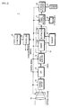
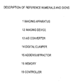
- Fig. 2 shows an example of configuration of an imaging apparatus 1 in accordance with the embodiment of the invention.
- the imaging apparatus 1 light incident through an optical system 10 and a mechanical shutter 11 is received by an imaging device 12, and is converted to electric signal (imaging signal) by photoelectric conversion.
- the imaging signal is subjected to signal processing and converted to digital signal (digital imaging signal) by an A/D converter 13.
- a shutter other than mechanical shutter, such as liquid crystal shutter, may also be used.
- the digital imaging signal is subjected to processing as described later by a digital clamper 14, an adder/subtractor 15, and a memory 16, then is subjected to a predetermined image processing by a image signal processor 17, and then is recorded to a recording media in a storage processor 18.
- the recording media may be a non-volatile rewritable memory 21.
- the image signal processor 17 also provides image data to be displayed on a viewfinder 20 for the purpose of confirming a captured image and the like.
- a controller 19 controls the whole of the imaging apparatus 1.
- the controller 19 includes a CPU (central processing unit), a ROM (read only memory), a RAM (random access memory), and a synchronizing signal generator for generating synchronizing signal used for drive control of the imaging device and timing control (frame-by-frame, pixel-by-pixel, etc.).
- the CPU controls various components of the imaging apparatus 1 using the RAM as work memory, according to a program stored in the ROM.
- a UI section 25 includes a release button for starting imaging and several controls for setting various functions of the imaging apparatus 1, such as shutter speed, aperture, zooming, and focusing, and outputs control signals based on the operation performed on these controls to the controller 19.
- the optical system 10 includes a lens system, an aperture mechanism, a focusing mechanism, a zooming mechanism and the like, in which aperture, focusing, zooming and the like are controlled based on the control by the controller 19 or based on manual operation.
- the mechanical shutter 11 can block the light path between the lens system 10 and the imaging device 12, and physically blocks light incident on the imaging device 12. For example, when a user presses down the release button (not shown), the mechanical shutter 11 is controlled to open by the controller 19, and light is incident on the imaging device 11 through the optical system 10.
- the mechanical shutter 11 is controlled to automatically become closed when a predetermined time elapses from becoming open, for example, according to a preset shutter speed.
- the imaging device 12 may be an image sensor employing CMOS (complementary metal-oxide semiconductor) (hereinafter abbreviated as CMOS).
- CMOS complementary metal-oxide semiconductor
- the imaging device 12 may also be a CCD (charge coupled device).
- the imaging device 12 is assumed to be a CMOS.
- the CMOS can control reading each pixel, and for example, can control reading pixel signals for each line.
- extracted charges are read, then the charges are reset. Both a rolling shutter and a global shutter can be used for the imaging device 12.
- exposure is started after reset for each line, and when exposure time ends, one line of pixel signals are output. Accordingly, exposure time for each line is shifted by one line between two consecutive lines.
- reset is performed in all lines at the same time, and exposure is started in all lines at the same time. Then reading signal charges from photodiodes to charge detectors is performed in the whole imaging area at the same time.
- the imaging device 12 outputs imaging signal for each pixel.
- the imaging signal output from the imaging device 12 is subjected to signal processing, such as noise suppression and gain control, by a signal processor (not shown) and is input to the A/D converter 13.
- the A/D converter 13 converts the imaging signal that is input as analog signal to digital signal with a quantization bit rate of X for each pixel.
- the digital imaging signal output from the A/D converter 13 is provided to the digital clamper 14.
- the digital clamper 14 digitally clamps the provided digital imaging signal and fixes its black signal level to a predetermined value. As an example, the digital clamper 14 subtracts the average of signals corresponding to several pixels to be used as optical black from signals each corresponding to each pixel of the digital imaging signal obtained by A/D converting the output of the imaging device 12.
- the digital imaging signal of which black signal level is fixed by the digital clamper 14 is provided to the adder/subtractor 15.
- the adder/subtractor 15 includes an adder section 15A and a subtractor section 15B, and performs, using the memory 16, accumulation of the provided digital imaging signals and subtraction between two accumulated data.
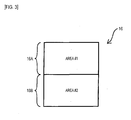
- the memory 16 includes a memory area 16A and a memory area 16B (shown as AREA #1 and AREA #2, respectively, in Fig.3 ), each of which can contain at least one frame of digital imaging signal.
- Each of the memory area 16A and the memory area 16B can be accessed pixel-by-pixel, and in which the number of bits allocated to one pixel is more than the quantization bit rate per pixel of the A/D converter 13. For example, if the A/D converter 13 A/D converts one pixel data with a quantization bit rate of 14 to output, at least 15 bits are allocated to one pixel in the memory areas 16A and 16B. More preferably, much more bits are allocated to one pixel.
- Fig. 4 shows an example of configuration of the adder/subtractor 15.
- the adder section 15A includes an adder 30 and switches 31 and 32.
- the subtractor section 15B includes a subtractor 33.
- the word length (the number of bits) of the adder 30 is at least longer than the quantization bit rate for each pixel of the A/D converter 13.
- the switches 31 and 32 select the memory area 16A or 16B.
- the switches 31 and 32 select output terminals 31A and 32A, respectively.
- the digital imaging signal provided to the adder/subtractor 15 is provided to one input terminal of the adder 30.
- data is read from the memory area 16A and provided to the other input terminal of the adder 30 through the switch 32.
- the adder 30 adds the digital imaging signal input to the one input terminal to the data input to the other input terminal.
- the result of addition by the adder 30 is overwritten to the memory area 16A through the switch 31. Note that the adder 30 performs addition between two data corresponding to each pixel.
- the number of bits allocated to one pixel is more than the quantization bit rate for each pixel of the A/D converter 13. This can reduce data clipping due to carry and data rounding error that may occur when the accumulation of digital imaging signals is performed.
- data read from the memory area 16A for each pixel is provided to one input terminal of the subtractor 33.
- data read from the memory area 16B for each pixel is provided to the other input terminal of the subtractor 33.
- the subtractor 33 subtracts the data input to the other input terminal from the data input to the one input terminal.
- the subtractor 33 performs subtraction, for example, between two data corresponding to each pixel.
- the digital imaging signal output from the adder/subtractor 15 is provided to the image signal processor 17.
- the image signal processor 17 converts the provided digital imaging signal to image data in a predetermined format and performs image processing, such as image quality correction, on the image data.
- the image data output from the image signal processor 17 is provided to the storage processor 18.
- the storage processor 18 compression-encodes the provided image data using a given compression encoding method such as JPEG (Joint Photographic Experts Group) method, and records the encoded data to a recording media such as the memory 21.
- JPEG Joint Photographic Experts Group
- FIG. 5 An example of imaging operation in the imaging apparatus 1 configured as the above is described with reference to a timing chart shown in Fig. 5 .
- the shutter speed is one minute and exposure is performed for three divided exposure times (20 sec each) into which the one minute is divided, during which the release button is pressed down and the mechanical shutter is open.
- the release button is pressed down and ON (see Fig. 5A ).
- the release button automatically becomes OFF when a period of time corresponding to the shutter speed elapses from becoming ON.
- the mechanical shutter 11 becomes open (see Fig. 5B ), the imaging device 12 is irradiated with light from the object through the optical system 10, and the imaging device 12 is exposed in the non-light-shielded condition.
- the controller 19 when the release button is pressed down, the controller 19 generates a vertical synchronizing signal VD (see Fig. 5C ) and provides it to the imaging device 12.
- VD vertical synchronizing signal
- the imaging device 12 In response to the vertical synchronizing signal VD, the imaging device 12 causes charges stored in all pixels to be output at the same time using global shutter function (GSH) and resets charges in all the pixels.
- GSH global shutter function
- the vertical synchronizing signal VD at time t 2 causes memory content of the memory 16 in the memory areas 16A and 16B to be cleared, because this is the first time for the pixels to be read since pressing down the release button.
- the timing for clearing the memory should be before the start of data accumulation in the memory 16 at the latest.
- the memory may be cleared when the release button is pressed down, which is not limited to the first reading of the pixels.
- the imaging device 12 In response to the vertical synchronizing signal VD, the imaging device 12 causes charges stored in the pixels to be read sequentially line-by-line using rolling shutter function (RSH) (see Fig. 5D ) and outputs them as imaging signal. In each pixel of which stored charge has been read out, storing charge is started immediately after the readout.
- RSH rolling shutter function
- the imaging signal output from the imaging device 12 sequentially line-by-line is A/D converted by the A/D converter 13 to digital imaging signal with a quantization bit rate of X per pixel. Then the digital imaging signal is clamped by the digital clamper 14 and its black signal level is fixed. This clamping by the digital clamper 14 implements the process of subtracting the dark current component "dark" of the imaging device from the imaging signal as described with reference to Fig. 1 .
- the digital imaging signal clamped by the digital clamper 14 is provided to the adder/subtractor 15 and accumulatively written to the memory 16 (see Fig. 5E ).
- the mechanical shutter 11 is open and the imaging device 12 is exposed to light from the object. That is, at this time, the digital imaging signal corresponds to the above-described non-light-shielded image signal.
- the terminals 31A and 32A are selected by the switches 31 and 32, respectively.
- the digital imaging signal is provided to one input terminal of the adder 30.
- data read from the memory area 16A of the memory 16 is provided to the other input terminal of the adder 30.
- the memory content of the memory 16 has been cleared since time t 1 , and value "0" is provided to the other input terminal of the adder 30 for each pixel.
- the adder 30 performs addition between two data provided to both the input terminals for each pixel. The result of addition is overwritten to the memory area 16A through the switch 31.
- Time t 4 is, for example, the point at which the mechanical shutter 11 transitions from open to closed.
- the imaging device 12 becomes exposed in the mechanically closed condition, that is, with the imaging device 12 shielded from light.
- the imaging device 12 is shielded from light and exposed for almost the same period of time as that during which the mechanical shutter 11 was open and the imaging device 12 was exposed to light from the object (one minute in this example).
- the process of adding the results of subtraction of the dark current component "dark" from the light-shielded image signals is performed.
- the exposure with the mechanical shutter 11 closed is performed almost similarly to that with the imaging device 12 irradiated with light from the object as described above.
- the controller 19 At time t 5 , when a predetermined period of time has elapsed from time t 4 at which charges stored in the pixels during the last divided exposure time with the imaging device 12 exposed to light are read, the controller 19 generates a vertical synchronizing signal VD (see Fig. 5C ) and provides it to the imaging device 12.
- the imaging device 12 causes charges stored in all the pixels to be output at the same time using global shutter function and starts storing charges in each pixel immediately (see Fig. 5D ).
- the controller 19 At time t 6 , when a predetermined period of time (20 seconds in this example) corresponding to the divided exposure time of the exposure for the non-light-shielded image signal has elapsed from time t 5 , the controller 19 generates another vertical synchronizing signal VD and provides it to the imaging device 12.
- the imaging device 12 In response to the vertical synchronizing signal VD, the imaging device 12 causes charges stored in the pixels to be read sequentially line-by-line using rolling shutter function (see Fig. 5D ) and outputs them as imaging signal. In each pixel of which stored charge has been read out, storing charge is started immediately after the readout.
- the imaging signal output from the imaging device 12 is converted to digital imaging signal with a quantization bit rate of X per pixel by the A/D converter 13. Then the digital imaging signal is clamped by the digital clamper 14 and its black signal level is fixed. The digital imaging signal with the black signal level fixed is provided to the adder/subtractor 15, and accumulatively written to the memory 16 for each pixel, as described above. The digital imaging signal obtained through exposure with the imaging device 12 shielded from light is written to the memory area 16B of the memory 16.
- the terminals 31B and 32B are selected by the switches 31 and 32, respectively.
- the digital imaging signal is provided to one input terminal of the adder 30.
- data read from the memory area 16B of the memory 16 is provided to the other input terminal of the adder 30.
- the memory content of the memory 16 has been cleared since time t 1 , and value "0" is provided to the other input terminal of the adder 30 for each pixel.
- the adder 30 performs addition between two data provided to both the input terminals for each pixel. The result of addition is overwritten to the memory area 16B through the switch 31.
- data corresponding to each pixel are read from the memory area 16A and 16B, and provided to one terminal and the other terminal of the subtractor 33, respectively.
- the subtractor 33 subtracts the data provided to the other input terminal from the data provided to the one input terminal to output. This process is performed on all of one frame of pixel data written to the memory area 16A and the memory area 16B. This effectively removes white spots due to a fixed pattern of the imaging device 12 and allows obtaining captured image data in which degradation of dynamic range due to accumulation of the dark current component is reduced.
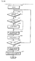
- Fig. 6 is a flowchart showing an example of exposure process in accordance with the embodiment of the invention. Determinations in the flowchart are performed, for example, by the controller 19 according to a given program.
- step S21 of Fig. 7A exposure time per image is set to three minutes, five minute or the like at the factory.
- a user sets the shutter speed (mechanical shutter speed) to, e.g., 60 minutes (step S22).
- step S31 the number of divided exposure times is set to, e.g., 20 at the factory.
- step S32 when performing imaging, the user sets the shutter speed to, e.g., 60 minutes.
- the shutter speed need not be preset. Instead, as shown in step S41 of Fig. 8 , one divided exposure time is preset, and exposure is finished when the release button is released.
- step S10 the timing of reading charges from the imaging device 12 is waited for. If determined that it is the timing of reading, the controller 19, for example, generates a vertical synchronizing signal VD and provides it to the imaging device 12.
- step S11 it is determined whether or not the charges read from the imaging device 12 at this timing are ones that have been stored through the first exposure since pressing down the release button. For example, the charges read from the imaging device 12 at time t 2 of Fig. 5 are determined to be ones that have been stored through the first exposure since pressing down the release button.
- step S11 if determined not to be the ones that have been stored through the first exposure, the process jumps to step S13. On the other hand, if determined to be the ones that have been stored through the first exposure, the process proceeds to step S12, then the memory content of the memory 16 is cleared, and then the process proceeds to step S13.
- step S13 it is determined whether the exposure was performed with the imaging device 12 irradiated with light from the object or with the imaging device 12 shielded from light. If determined that the exposure was performed with the imaging device 12 irradiated with light from the object, the process proceeds to step S14. On the other hand, if determined that the exposure was performed with the imaging device 12 shielded from light, the process proceeds to step S15.
- step S14 the non-light-shielded image signal that is digital imaging signal obtained through the exposure performed with the imaging device 12 irradiated with light from the object is provided to the adder/subtractor 15 and accumulatively written to the memory area 16A of the memory 16 as described above.
- step S15 the light-shielded image signal that is digital imaging signal obtained through the exposure performed with the imaging device 12 shielded from light is provided to the adder/subtractor 15 and accumulatively written to the memory area 16B of the memory 16 as described above.
- step S16 it is determined whether or not the predetermined number of times of exposure according to the set number of divided exposure times have been finished. If determined that the predetermined number of times of exposure have not been finished yet, the process returns to step S10 and another timing of reading charges from the imaging device 12 is waited for.
- step S17 in the adder/subtractor 15, according to Equation (3) described above, the process of subtracting the light-shielded image signal accumulatively written to the memory area 16B from the non-light-shielded image signal accumulatively written to the memory area 16A is performed for each pixel. This subtraction process for each pixel is performed on all of one frame of pixel data written to the memory area 16A and the memory area 16B.
- Fig. 9A the process steps corresponding to the steps S10, S11, S12, and S14 in Fig. 6 are shown as steps S110, S111, S112, and S114, respectively.
- step S101 the count value CNT1, which means the number of performing exposure for one divided exposure time, is initialized to 0. Then exposure in the non-light-shielded condition is performed similarly to the process shown in the flowchart of Fig. 6 .
- step S102 the count value CNT1 is incremented and stored every time exposure is performed for one divided exposure time. Then, if determined in step S103 that the release button is released, the addition of non-light-shielded image signals is performed in the memory area #1 in step S104.
- step S201 the count value CNT2, which means the number of performing exposure for one divided exposure time, is initialized to 0.
- step S202 the count value CNT2 is incremented and stored every time exposure is performed for one divided exposure time.
- step S203 determines whether CNT1 equals CNT2 or that CNT1 equals CNT2, the addition result of light-shielded image signals stored in the memory area #2 is subtracted from the addition result of non-light-shielded image signals stored in the memory area #1 in step S217.
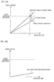
- Fig. 10 to 12 An example of an advantage of the above-described control in accordance with the embodiment of the invention is described with reference to Fig. 10 to 12 .
- An example of an advantage of subtracting the dark current component "dark" every time exposure is performed for one divided exposure time and accumulating the digital imaging signals is described with reference to Fig. 10 .
- the object signal component is assumed to be signal component that is captured image signal based on the output of the imaging device 12 from which noise component due to a fixed pattern of the imaging device 12 and the dark current component "dark" are removed.
- the object signal component as well as the dark current component are accumulated to increase as exposure time increases.
- the non-light-shielded image signal component that is the sum of the object signal component and the dark current component reaches X bits that is the maximum output signal level of the A/D converter at exposure time et, and the level of the non-light-shielded image signal component is saturated and clipped at exposure time et or later. Consequently, the dynamic range of the object signal is significantly reduced at exposure time et or later.
- the dark current component is subtracted from the object signal component every time exposure for one divided exposure time is performed. Accordingly, the dark current component "dark" is removed before the non-light-shielded image signal component reaches the maximum output signal level of the A/D converter, only the object signal component can be accumulated as the non-light-shielded image signal, and the dynamic range can be ensured as illustrated in Fig. 10B .
- the non-light-shielded image signal is a composite signal of the object signal component based on light from the object and the noise component based on a fixed pattern of the imaging device 12.
- the object signal component as well as the noise component based on the fixed pattern are accumulated to increase as exposure time increases.
- the dynamic range of the object signal component will be compressed by the accumulated noise component.
- the non-light-shielded image signal is obtained through exposure with the mechanical shutter 11 open, then the light-shielded image signal is obtained through exposure with the mechanical shutter 11 closed for almost the same exposure time as with the non-light-shielded image signal.
- the light-shielded image signal is only the accumulated noise component based on the fixed pattern of the imaging device 12.
- FIG. 12 An example of an advantage of allocating the number of bits to one pixel in the memory 16 used for accumulating the digital imaging signal being more than the quantization bit rate for one pixel of the A/D converter 13, is described with reference to Fig. 12 .
- the line representing the non-light-shielded image signal component represents values in the memory area 16A
- the line representing the defect component represents values in the memory area 16B.
- the difference between the non-light-shielded image signal component in the memory area 16A and the defect component in the memory area 16B is the object signal component based on light from the object.
- the non-light-shielded image signal component accumulatively increases as exposure time increases, then in the memory area 16A, the accumulated non-light-shielded image signal component may be saturated, for example, at the data length of X bits at exposure time et, and the accumulated component of X bits or higher may be clipped at exposure time et or later. Then, at exposure time et or later, the dynamic range of the object signal component that is the result of subtracting the accumulated defect component from the accumulated non-light-shielded image signal component may be significantly reduced.
- the number of bits (Y bits) allocated to one pixel in the memory 16 is more than the quantization bit rate for one pixel of the A/D converter 13. As illustrated in Fig. 12B , this prevents the accumulated non-light-shielded image signal component from being saturated in the memory area 16A and ensures the dynamic range of the object signal component, even when long exposure is performed (see Fig. 12C ).
Landscapes
- Engineering & Computer Science (AREA)
- Multimedia (AREA)
- Signal Processing (AREA)
- Transforming Light Signals Into Electric Signals (AREA)
- Exposure Control For Cameras (AREA)
- Studio Devices (AREA)
Applications Claiming Priority (2)
| Application Number | Priority Date | Filing Date | Title |
|---|---|---|---|
| JP2007157183 | 2007-06-14 | ||
| PCT/JP2008/060723 WO2008153085A1 (ja) | 2007-06-14 | 2008-06-05 | 撮像装置、撮像制御方法および撮像制御プログラム |
Publications (2)
| Publication Number | Publication Date |
|---|---|
| EP2157784A1 true EP2157784A1 (de) | 2010-02-24 |
| EP2157784A4 EP2157784A4 (de) | 2011-03-09 |
Family
ID=40129690
Family Applications (1)
| Application Number | Title | Priority Date | Filing Date |
|---|---|---|---|
| EP08765494A Ceased EP2157784A4 (de) | 2007-06-14 | 2008-06-05 | Bildaufnahmevorrichtung, bildaufnahmeverfahren und bildaufnahmeprogramm |
Country Status (7)
| Country | Link |
|---|---|
| US (1) | US8237812B2 (de) |
| EP (1) | EP2157784A4 (de) |
| JP (1) | JP5229224B2 (de) |
| KR (1) | KR20100031599A (de) |
| CN (1) | CN101682699B (de) |
| MY (1) | MY151485A (de) |
| WO (1) | WO2008153085A1 (de) |
Families Citing this family (17)
| Publication number | Priority date | Publication date | Assignee | Title |
|---|---|---|---|---|
| JP5479202B2 (ja) * | 2010-04-28 | 2014-04-23 | キヤノン株式会社 | 撮像装置及び制御方法 |
| JP2012163522A (ja) * | 2011-02-09 | 2012-08-30 | Mitsui Optronics:Kk | 温度情報計測方法 |
| JP6021465B2 (ja) * | 2011-07-11 | 2016-11-09 | キヤノン株式会社 | 画像処理装置及び画像処理装置の制御方法 |
| WO2013054402A1 (ja) * | 2011-10-12 | 2013-04-18 | キヤノン株式会社 | 撮像装置及び撮像装置の制御方法 |
| JP5889324B2 (ja) * | 2011-10-12 | 2016-03-22 | キヤノン株式会社 | 撮像装置及び撮像装置の制御方法 |
| JP6053447B2 (ja) * | 2012-10-23 | 2016-12-27 | オリンパス株式会社 | 撮像装置 |
| JP6104060B2 (ja) * | 2013-06-06 | 2017-03-29 | オリンパス株式会社 | 撮像装置、撮像方法 |
| JP2015050671A (ja) * | 2013-09-02 | 2015-03-16 | 株式会社東芝 | 固体撮像装置 |
| CN103957364B (zh) * | 2014-04-01 | 2017-06-06 | 聚光科技(杭州)股份有限公司 | 一种ccd数据采集处理方法 |
| JP6418839B2 (ja) * | 2014-08-04 | 2018-11-07 | キヤノン株式会社 | 撮像装置及びその制御方法、プログラム、記憶媒体 |
| JP6746421B2 (ja) * | 2016-07-29 | 2020-08-26 | キヤノン株式会社 | 撮像装置 |
| JP2018072390A (ja) * | 2016-10-24 | 2018-05-10 | オリンパス株式会社 | 撮像装置 |
| KR20190114332A (ko) * | 2018-03-29 | 2019-10-10 | 에스케이하이닉스 주식회사 | 이미지 센싱 장치 및 그의 동작 방법 |
| US11950948B2 (en) | 2018-09-18 | 2024-04-09 | Hologic, Inc. | Systems and methods for mitigating imaging artifacts |
| CN111432093B (zh) * | 2020-03-19 | 2021-05-25 | 成都微光集电科技有限公司 | 一种cmos图像传感器的暗电流校正方法 |
| CN115174819B (zh) * | 2022-07-08 | 2023-11-03 | 重庆紫光华山智安科技有限公司 | 一种曝光控制方法、装置、设备及介质 |
| US12501183B2 (en) * | 2022-12-09 | 2025-12-16 | Samsung Electronics Co., Ltd. | Image sensor and operating method of image sensor |
Family Cites Families (20)
| Publication number | Priority date | Publication date | Assignee | Title |
|---|---|---|---|---|
| JP2565261B2 (ja) | 1987-10-17 | 1996-12-18 | ソニー株式会社 | 固体撮像装置用画像欠陥補正装置 |
| JP2990930B2 (ja) | 1992-03-18 | 1999-12-13 | ソニー株式会社 | 固体撮像装置 |
| JPH0795841B2 (ja) | 1992-04-21 | 1995-10-11 | オリンパス光学工業株式会社 | 画像記録装置 |
| JPH0851571A (ja) | 1994-08-03 | 1996-02-20 | Olympus Optical Co Ltd | 電子的撮像装置 |
| JP3840671B2 (ja) * | 1995-03-24 | 2006-11-01 | ソニー株式会社 | 撮像装置 |
| JPH0918793A (ja) * | 1995-06-26 | 1997-01-17 | Nikon Corp | 撮像装置 |
| US7023479B2 (en) | 2000-05-16 | 2006-04-04 | Canon Kabushiki Kaisha | Image input apparatus having addition and subtraction processing |
| JP2001326850A (ja) | 2000-05-16 | 2001-11-22 | Canon Inc | 撮像装置、その制御方法およびコンピュータ読み取り可能な媒体 |
| JP3897520B2 (ja) * | 2000-07-11 | 2007-03-28 | キヤノン株式会社 | 撮像装置および撮像装置の制御方法 |
| JP3931606B2 (ja) * | 2001-09-20 | 2007-06-20 | ソニー株式会社 | 撮像装置およびノイズ除去方法 |
| JP4027632B2 (ja) * | 2001-10-03 | 2007-12-26 | オリンパス株式会社 | 撮像装置 |
| US7167267B2 (en) * | 2001-12-19 | 2007-01-23 | Hewlett-Packard Development Company, L.P. | Noise reduction in an image capturing device |
| JP4017874B2 (ja) | 2002-01-28 | 2007-12-05 | 株式会社ニコンシステム | 電子カメラ |
| JP2004007048A (ja) * | 2002-05-30 | 2004-01-08 | Minolta Co Ltd | 撮像装置 |
| JP4532819B2 (ja) * | 2002-11-20 | 2010-08-25 | キヤノン株式会社 | 撮像装置 |
| JP4391782B2 (ja) | 2003-09-01 | 2009-12-24 | Hoya株式会社 | デジタルカメラのノイズリダクション装置 |
| JP4358606B2 (ja) * | 2003-11-20 | 2009-11-04 | オリンパス株式会社 | インターバル撮影に適用される撮像装置およびそのための暗時ノイズ抑圧処理方法 |
| JP4342926B2 (ja) * | 2003-12-24 | 2009-10-14 | 三菱電機株式会社 | 画像入力方法および画像入力装置 |
| JP3748267B2 (ja) * | 2004-06-16 | 2006-02-22 | ソニー株式会社 | 撮像装置 |
| JP2006108950A (ja) | 2004-10-04 | 2006-04-20 | Sony Corp | 撮像装置 |
-
2008
- 2008-06-05 CN CN2008800200299A patent/CN101682699B/zh not_active Expired - Fee Related
- 2008-06-05 WO PCT/JP2008/060723 patent/WO2008153085A1/ja not_active Ceased
- 2008-06-05 US US12/664,412 patent/US8237812B2/en not_active Expired - Fee Related
- 2008-06-05 KR KR1020107000080A patent/KR20100031599A/ko not_active Withdrawn
- 2008-06-05 EP EP08765494A patent/EP2157784A4/de not_active Ceased
- 2008-06-05 JP JP2009519294A patent/JP5229224B2/ja not_active Expired - Fee Related
- 2008-06-05 MY MYPI20095270 patent/MY151485A/en unknown
Also Published As
| Publication number | Publication date |
|---|---|
| US20100182451A1 (en) | 2010-07-22 |
| EP2157784A4 (de) | 2011-03-09 |
| KR20100031599A (ko) | 2010-03-23 |
| CN101682699B (zh) | 2012-10-10 |
| CN101682699A (zh) | 2010-03-24 |
| MY151485A (en) | 2014-05-30 |
| US8237812B2 (en) | 2012-08-07 |
| JPWO2008153085A1 (ja) | 2010-08-26 |
| WO2008153085A1 (ja) | 2008-12-18 |
| JP5229224B2 (ja) | 2013-07-03 |
Similar Documents
| Publication | Publication Date | Title |
|---|---|---|
| EP2157784A1 (de) | Bildaufnahmevorrichtung, bildaufnahmeverfahren und bildaufnahmeprogramm | |
| JP4742359B2 (ja) | 動画撮像装置及びそのプログラム | |
| JP5219778B2 (ja) | 撮像装置及びその制御方法 | |
| US7042507B2 (en) | Digital camera, pixel data read-out control apparatus and method, blur-detection apparatus and method | |
| JP2005130045A (ja) | 撮像装置及びこれに用いる撮像素子 | |
| JP2003204486A (ja) | 撮像装置 | |
| CN101656819B (zh) | 图像拍摄装置及减少拖尾的方法 | |
| JP2003158680A (ja) | 撮像装置 | |
| JP5013811B2 (ja) | 撮像装置及び補正方法 | |
| JP5094252B2 (ja) | 撮像装置及びその制御方法 | |
| JP5013812B2 (ja) | 撮像装置及び補正方法 | |
| JP3616870B2 (ja) | 撮像装置及びその信号処理方法 | |
| JP2002027300A (ja) | デジタルカメラ | |
| JP2007300368A (ja) | 固体撮像装置 | |
| JP4416812B2 (ja) | 撮像装置 | |
| JP4735994B2 (ja) | 撮像装置及び方法、プログラム、並びに記録媒体 | |
| JP2009260871A (ja) | 撮像装置 | |
| JP5400432B2 (ja) | 撮像装置、その制御方法及びカメラ | |
| JP5106056B2 (ja) | 撮像装置及びそのフリッカ検出方法 | |
| JP4306653B2 (ja) | 撮像装置及びその信号処理方法 | |
| JP2006014163A (ja) | 固体撮像装置およびスミア補正方法 | |
| JP3788449B2 (ja) | 撮像装置及びその信号処理方法 | |
| JP4322258B2 (ja) | ノイズ処理装置および撮像装置 | |
| JP4341531B2 (ja) | 撮像装置及びその信号処理方法 | |
| JP4847281B2 (ja) | 撮像装置及びその制御方法並びに撮像システム |
Legal Events
| Date | Code | Title | Description |
|---|---|---|---|
| PUAI | Public reference made under article 153(3) epc to a published international application that has entered the european phase |
Free format text: ORIGINAL CODE: 0009012 |
|
| 17P | Request for examination filed |
Effective date: 20091210 |
|
| AK | Designated contracting states |
Kind code of ref document: A1 Designated state(s): AT BE BG CH CY CZ DE DK EE ES FI FR GB GR HR HU IE IS IT LI LT LU LV MC MT NL NO PL PT RO SE SI SK TR |
|
| AX | Request for extension of the european patent |
Extension state: AL BA MK RS |
|
| DAX | Request for extension of the european patent (deleted) | ||
| A4 | Supplementary search report drawn up and despatched |
Effective date: 20110204 |
|
| 17Q | First examination report despatched |
Effective date: 20110805 |
|
| REG | Reference to a national code |
Ref country code: DE Ref legal event code: R003 |
|
| STAA | Information on the status of an ep patent application or granted ep patent |
Free format text: STATUS: THE APPLICATION HAS BEEN REFUSED |
|
| 18R | Application refused |
Effective date: 20130221 |