EP2158676B1 - Umschaltbare mehrband-lna-konstruktion - Google Patents
Umschaltbare mehrband-lna-konstruktion Download PDFInfo
- Publication number
- EP2158676B1 EP2158676B1 EP08759747.2A EP08759747A EP2158676B1 EP 2158676 B1 EP2158676 B1 EP 2158676B1 EP 08759747 A EP08759747 A EP 08759747A EP 2158676 B1 EP2158676 B1 EP 2158676B1
- Authority
- EP
- European Patent Office
- Prior art keywords
- section
- output
- input
- circuit
- low noise
- Prior art date
- Legal status (The legal status is an assumption and is not a legal conclusion. Google has not performed a legal analysis and makes no representation as to the accuracy of the status listed.)
- Active
Links
Images



Classifications
-
- H—ELECTRICITY
- H03—ELECTRONIC CIRCUITRY
- H03F—AMPLIFIERS
- H03F1/00—Details of amplifiers with only discharge tubes, only semiconductor devices or only unspecified devices as amplifying elements
- H03F1/08—Modifications of amplifiers to reduce detrimental influences of internal impedances of amplifying elements
- H03F1/22—Modifications of amplifiers to reduce detrimental influences of internal impedances of amplifying elements by use of cascode coupling, i.e. earthed cathode or emitter stage followed by earthed grid or base stage respectively
- H03F1/223—Modifications of amplifiers to reduce detrimental influences of internal impedances of amplifying elements by use of cascode coupling, i.e. earthed cathode or emitter stage followed by earthed grid or base stage respectively with MOSFET's
-
- H—ELECTRICITY
- H03—ELECTRONIC CIRCUITRY
- H03F—AMPLIFIERS
- H03F1/00—Details of amplifiers with only discharge tubes, only semiconductor devices or only unspecified devices as amplifying elements
- H03F1/34—Negative-feedback-circuit arrangements with or without positive feedback
- H03F1/342—Negative-feedback-circuit arrangements with or without positive feedback in field-effect transistor amplifiers
-
- H—ELECTRICITY
- H03—ELECTRONIC CIRCUITRY
- H03F—AMPLIFIERS
- H03F1/00—Details of amplifiers with only discharge tubes, only semiconductor devices or only unspecified devices as amplifying elements
- H03F1/42—Modifications of amplifiers to extend the bandwidth
-
- H—ELECTRICITY
- H03—ELECTRONIC CIRCUITRY
- H03F—AMPLIFIERS
- H03F1/00—Details of amplifiers with only discharge tubes, only semiconductor devices or only unspecified devices as amplifying elements
- H03F1/56—Modifications of input or output impedances, not otherwise provided for
-
- H—ELECTRICITY
- H03—ELECTRONIC CIRCUITRY
- H03F—AMPLIFIERS
- H03F3/00—Amplifiers with only discharge tubes or only semiconductor devices as amplifying elements
- H03F3/189—High-frequency amplifiers, e.g. radio frequency amplifiers
- H03F3/19—High-frequency amplifiers, e.g. radio frequency amplifiers with semiconductor devices only
- H03F3/195—High-frequency amplifiers, e.g. radio frequency amplifiers with semiconductor devices only in integrated circuits
-
- H—ELECTRICITY
- H03—ELECTRONIC CIRCUITRY
- H03F—AMPLIFIERS
- H03F3/00—Amplifiers with only discharge tubes or only semiconductor devices as amplifying elements
- H03F3/72—Gated amplifiers, i.e. amplifiers which are rendered operative or inoperative by means of a control signal
-
- H—ELECTRICITY
- H03—ELECTRONIC CIRCUITRY
- H03F—AMPLIFIERS
- H03F2200/00—Indexing scheme relating to amplifiers
- H03F2200/111—Indexing scheme relating to amplifiers the amplifier being a dual or triple band amplifier, e.g. 900 and 1800 MHz, e.g. switched or not switched, simultaneously or not
-
- H—ELECTRICITY
- H03—ELECTRONIC CIRCUITRY
- H03F—AMPLIFIERS
- H03F2200/00—Indexing scheme relating to amplifiers
- H03F2200/151—A source follower being used in a feedback circuit of an amplifier stage
-
- H—ELECTRICITY
- H03—ELECTRONIC CIRCUITRY
- H03F—AMPLIFIERS
- H03F2200/00—Indexing scheme relating to amplifiers
- H03F2200/222—A circuit being added at the input of an amplifier to adapt the input impedance of the amplifier
-
- H—ELECTRICITY
- H03—ELECTRONIC CIRCUITRY
- H03F—AMPLIFIERS
- H03F2200/00—Indexing scheme relating to amplifiers
- H03F2200/294—Indexing scheme relating to amplifiers the amplifier being a low noise amplifier [LNA]
-
- H—ELECTRICITY
- H03—ELECTRONIC CIRCUITRY
- H03F—AMPLIFIERS
- H03F2200/00—Indexing scheme relating to amplifiers
- H03F2200/306—Indexing scheme relating to amplifiers the loading circuit of an amplifying stage being a parallel resonance circuit
-
- H—ELECTRICITY
- H03—ELECTRONIC CIRCUITRY
- H03F—AMPLIFIERS
- H03F2200/00—Indexing scheme relating to amplifiers
- H03F2200/378—A variable capacitor being added in the output circuit, e.g. collector, drain, of an amplifier stage
-
- H—ELECTRICITY
- H03—ELECTRONIC CIRCUITRY
- H03F—AMPLIFIERS
- H03F2200/00—Indexing scheme relating to amplifiers
- H03F2200/429—Two or more amplifiers or one amplifier with filters for different frequency bands are coupled in parallel at the input or output
-
- H—ELECTRICITY
- H03—ELECTRONIC CIRCUITRY
- H03F—AMPLIFIERS
- H03F2200/00—Indexing scheme relating to amplifiers
- H03F2200/451—Indexing scheme relating to amplifiers the amplifier being a radio frequency amplifier
-
- H—ELECTRICITY
- H03—ELECTRONIC CIRCUITRY
- H03F—AMPLIFIERS
- H03F2203/00—Indexing scheme relating to amplifiers with only discharge tubes or only semiconductor devices as amplifying elements covered by H03F3/00
- H03F2203/72—Indexing scheme relating to gated amplifiers, i.e. amplifiers which are rendered operative or inoperative by means of a control signal
- H03F2203/7209—Indexing scheme relating to gated amplifiers, i.e. amplifiers which are rendered operative or inoperative by means of a control signal the gated amplifier being switched from a first band to a second band
Definitions
- the present invention relates to a low area LNA technique applicable for switched multiband LNA design, particular in digital CMOS.
- Broadband amplifiers are commonly used as a low area solution for the integration of LNAs for multistandard receivers, as in R. Bagheri et al., "An 800-MHz-6-GHz Software-Defined Wireless Receiver in 90-nm CMOS", IEEE JSSC, Vol. 41, No. 12, pp. 2860-2876, December 2006 .
- CMOS complementary metal-oxide-semiconductor
- inductor-less designs attain bandwidths above 6 GHz.
- Their broadband nature however, imposes high linearity demands on both the LNA and at system level.
- separate narrowband LNAs relax linearity concerns significantly. While this solution allows optimized performance in each band, the area consumption forms a serious drawback.
- Multiband LNAs e.g. H. Hashemi, A.
- a broadband LNA circuit is disclosed by Andersson, S. et al. in "Wideband LNA for a Multistandard Wireless Receiver in 0.18 ⁇ m CMOS", European Solid-state Circuits, Piscataway, NJ, USA, IEEE, 16 September 2003, pp. 655-658 .
- the circuit comprises an inductor as part of the load.
- the frequency band in which the amplifier operates is however determined by an inductor at the input.
- It is an aim of the present invention is to provide a low noise amplifier which consumes less design area.
- a low noise amplifying circuit comprising a feedback amplifier which comprises an amplifying section, preferably a low-noise amplifying section, for amplifying signals between the input and the output of the circuit.
- the amplifying section comprises an input transistor and an output or cascade transistor.
- the feedback amplifier is provided with a feedback means arranged for providing input matching from the output to the input.
- the LNA circuit further comprises at least one frequency band determining inductive section, i.e. a circuit part having a predetermined resonance frequency for influencing at least one frequency band in which the amplifying section operates.
- the/each frequency band determining inductive section is directly connected to the output of the circuit and the feedback means provides a feedback connection for the section(s) to the input.
- the at least one frequency band in which the amplifying section operates is substantially completely determined by the at least one frequency band determining inductive section.
- each frequency band determining inductive section is the circuit part which in operation mainly determinates the frequency band in which signals are amplified, i.e. that the influence of any other components active in the circuit on the respective frequency band is neglectable.
- inductive section is intended to mean a circuit part comprising one or more inductive components and one or more capacitive or resistive components.
- the output behavior is fed back to the input.
- This active feedback ensures input matching maintaining a low noise figure (NF).
- NF noise figure
- this feedback is exploited and made narrowband by adding at least one inductive section with a predetermined resonance frequency to its load (narrowband gain and thus filtering).
- the output of the amplifier is a noise-insensitive node, so low area, low-Q inductors can be selected to be placed here.
- Low area, low-Q inductors in a digital back-end of line can now replace high-Q, large area, thick metal demanding inductors typically used in the prior art designs. This is possible since the inductive section(s) determining the frequency band(s) is/are maintained at noise-insensitive nodes.
- the/each inductive section comprises an inductor, preferably a stacked multilayer inductor.
- inductors can achieve very high inductance values at very low area, for a low Q. Resonance frequencies above 10 GHz are attainable.
- the inductor can be co-designed with the circuit to choose the Q as a function of the desired load. Very appealing is that this type of inductor can be realized in any digital back-end-of-line (BEOL) with a sufficient number of layers. No RF BEOL is needed, as the inductor is pushed to a location in the circuit where it is rather uncritical for noise.
- BEOL digital back-end-of-line
- the feedback means comprises a feedback transistor.
- the feedback transistor comprises a transistor in series with one or more feedback resistors. This design can minimize the nonlinearities generated by the feedback transistor. Any other feedback means known to the person skilled in the art may also be used.
- the circuit comprises a plurality of different inductive sections with different resonance frequencies, which are switchably connected to the output (meaning that the direct connection to the output is switchable), hence providing a switchable multiband low noise amplifying circuit.
- an inductor with its predetermined resonance frequency can be selected and can be switchably connected to the output. Additionally, all switching is preferably performed at noise-insensitive nodes.
- the input and output transistor forming the amplifying section preferably together form a cascode amplifier.
- any other low noise amplifier topology known to the person skilled in the art may also be used, e.g. two cascaded common source transistors.
- the low noise amplifying circuit comprises a plurality of sections, each forming a separate feedback amplifier as described above with the input transistor in common.
- Each section has its own inductive section, connected at the respective output.
- the inductive sections of the different amplifier sections preferably have different resonance frequencies determining the frequency bands in which the circuit is operable.
- Each inductive section preferably comprises a low-area, low-Q inductor placed at a noise-insensitive node.
- Each section operates in a predetermined narrowband.
- a plurality of these sections is switchably connected to the first input transistor, which is common for the sections, providing a switchable concurrent multiband low noise amplifying circuit. For example, switching on two sections can provide a dual-band LNA constructed with miniature size LNA sections. As the area of each section can be very low, adding more bands by adding sections can go relatively unpunished as compared to other LNA solutions.
- one or more of the amplifier sections is controlled by one or more varactors providing a wide frequency tuning range. Even for a limited varactor tuning range, a wide band can be covered and the circuit can benefit from inherent filtering as opposed to a wideband solution.
- the invention further relates to a multimode receiver comprising a low noise amplifying circuit as proposed above.
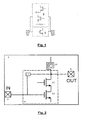
- Fig.1 shows a design comprising an amplifier ( 1 ) and a feedback amplifier ( 2 ).
- This design is known in the state of art as a shunt-shunt amplifier. It is known in the state of art that a shunt-shunt feedback amplifier employs feedback to obtain adequate input matching for a low noise figure (NF). Active feedback ensures input matching maintaining a low NF. It can be made narrow-band by adding an inductor L LOAD to its load.
- NF noise figure
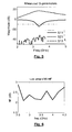
- a design according to the invention is shown in fig.2 : a low noise amplifying circuit ( 3 ) comprising a feedback amplifier ( 4 ) and an inductive section with inductor ( 15 ).
- the feedback amplifier ( 4 ) comprises an input transistor ( 11 ) and an output transistor ( 12 ) forming an LNA between an input ( 5 ) and an output ( 6 ) of the circuit.
- the feedback amplifier further comprises a feedback means ( 7 ), providing input matching.
- the inductor ( 15 ) is connected to the output ( 6 ) of the feedback amplifier ( 4 ) and to the input ( 5 ) via said feedback means ( 7 ).
- the inductor has a predetermined resonance frequency, chosen such that it determines the frequency band in which the LNA operates. According to the invention, preferably all inductive components determining frequency bands in which the LNA operates are connected at the output side, i.e. the noise insensitive node.
- a low noise amplifier comprising an input ( 11 ) and a cascode transistor ( 12 ) and a bias current source (or source follower) ( 13 ), is connected to a feedback transistor ( 14 ).
- an inductor L LOAD 15
- This inductor resonating with the total load capacitance C LOAD , also relaxes voltage headroom problems present in the circuit, as no voltage drop over a resistive load is needed.
- the load inductor is preferably a stacked multilayer inductor ( 16 ). The stacked inductor uses several planar windings in several consecutive metal layers.
- the noise factor F is approximately given by: F ⁇ 1 + ⁇ 1 g mMn ⁇ 1 ⁇ R S + ⁇ 2 1 + g mMn ⁇ 1 ⁇ R LOAD + 1 g mMn ⁇ 1 2 ⁇ R LOAD ⁇ R S + R S R Bias in which ⁇ 1 and ⁇ 2 are the noise excess factors. From equation (3) we see that a large g mMn1 is needed to lower the noise. Clearly, the contribution of the inductor - the fourth term in (3) - is suppressed when this large input transconductance is present. The g mMn1 has a higher relative impact than the lowered R LOAD caused by the use of a low-Q inductor.
- the IIP3 of the wideband LNA without the inductor would be approximately: IIP ⁇ 3 ⁇ 4 1 + A V ⁇ 2 3 ⁇ K 2 ⁇ gmMn ⁇ 2 g mMn ⁇ 2 2 + K 3 ⁇ gmMn ⁇ 2 g mMn ⁇ 2 where K 2gmMn2 and K 3gmMn2 are the slope and the curvature of g mMn2 as a function of v GS .
- K 2gmMn2 generates most of the second-order distortion at the input of the circuit, since the signal at the gate of M n2 is large (this is the output of the circuit). This distortion propagates linearly to the output, where the second-order nonlinearity K 2gmMn2 combines it in turn with the fundamental of the output signal to generate third-order distortion at the input. Finally, this third-order distortion propagates linearly to the output.
- the second-order distortion generated by M n2 reaches the output heavily suppressed, and is hindered to generate third-order distortion.
- Third-order distortion generated by K 3gmMn2 is not suppressed by this filtering. Thanks to the lower contribution of K 2gmMn2 , the linearity of the feedback LNA is improved as compared to the wideband (unfiltered) version.
- the circuit has been implemented in a 0.13 ⁇ m CMOS technology, using a low power supply of 1 V. Note that the proposed technique may be implemented in any of the technologies known to the person skilled in the art, even in e.g. BiCMOS.
- a sufficiently high value for g mMn1 has been chosen for a reasonably low noise figure, while input matching is preserved by g mMn2 .
- a relatively high overdrive for M n1 keeps the input pole at high frequencies since it lowers C gs of M n1 for a given value of g mMn1 .
- R LOAD parasitic resistance
- For the inductor 4.5 windings over 4 layers (M3-M6) are used. The inductor occupies an area of only 40x40 ⁇ m 2 .
- a source follower ( 13 ) is employed to drive the 50 ⁇ load of the measurement equipment.
- Fig.4 shows a chip micrograph on the left, indicating the very small area consumption (the size of a bondpad) of the complete LNA. On the right side of fig.4 , a zoom of the LNA is depict, showing the stacked inductor along with the LAN core and buffer.
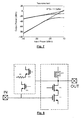
- Fig. 5 and Fig. 6 show the measured S-parameters and NF.
- a voltage gain of 20.8 dB is achieved with a 2.2 dB NF and a return loss below -10 dB around 3.4 GHz.
- the power gain S 21 is 16.8 dB, including the source follower buffer driving the 50 ⁇ for measurement purposes, adding a loss of about 4 dB.
- the LNA would drive a mixer, and the buffer would not be needed.
- the voltage gain is thus about 20.8 dB.
- the buffer consumes an additional 3.5 mW.
- Fig.7 shows the two-tone test measurement results for a 3.45 GHz and 3.4 GHz excitation.
- the measured IIP3 is -11.5 dBm. Note that, if necessary, linearity can be increased as explained in the above sections.
- the LNA design with a feedback resistor ( 61 ) is shown in fig. 8 .
- Table 1 lists some recently published fully integrated narrowband LNA designs.
- the design of the invention offers the best NF for a high gain, and the lowest area consumption while not using the most advanced technology. This LNA is by far the smallest published narrowband LNA in CMOS.
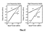
- FIG. 9 A circuit implementation example wherein a high order load is employed for concurrent dual band operation is shown in fig. 9 .
- a feedback means comprising a transistor in series with a resistor ( 61 ). Narrowband gain and input matching is achieved concurrently at two frequencies.
- the proposed multiband LNA is derived from the narrowband 'bondpad size' shunt-shunt feedback amplifier. As these LNA implementations occupy a very low area, employing several versions for the different frequency bands on one chip would go relatively unpunished. Since the demands on the Q-factor of the output load are low, varactor tuning can provide additional band selection.
- Fig.10 shows a circuit implementation example wherein a varactor ( 64 ) is used. In particular, a switched output load is employed in combination with a varactor for additional tuning. Switches ( 62,63 ) control the output load. Alternative to the use of several versions, one can integrate them together.
- the switches ( 62, 63 ) are placed between the inductors ( 15 ) and the Vdd line. Alternatively, they may also be placed between the inductors ( 15 ) and the output ( Out ). In both alternatives, the inductors are understood to be switchably connected to the output, as their influence can be selectively removed from the circuit.
- the NF at resonance is approximately given by F ⁇ 1 + ⁇ 1 g mMn ⁇ 1 ⁇ R S + ⁇ 2 1 + g mMn ⁇ 1 ⁇ R LOAD + 1 g mMn ⁇ 1 2 ⁇ R LOAD ⁇ R S + R S R Bias in which ⁇ 1 and ⁇ 2 are the noise excess factors of M n1 ( 11 ) and M n2 ( 14 ) respectively. From this expression we note that a large g mMn1 is required to lower the noise, independent of the frequency.
- Switch SW 2 controls the ON/OFF state of the cascode transistor M nC ( 75,76 ) enabling or disabling current flow.
- a simple source follower buffer as shown in fig.12 , for measurement purposes. This buffer drives the 50 ⁇ measurement setup.
- a switch SW 1 sets the LNA output to a clean ground.
- M n2 71,72
- M n2,OFF is turned off, and does no longer influence the input matching.
- the third switch SW 3 ( 79,80 ) has as only purpose to avoid a DC loss current flowing through L LOAD in off-mode.
- SW 3 ( 79 , 80 ) is located at an AC ground position, in series with the low-Q inductor it can be sized not influencing RF performance at all. If necessary, a bypass capacitor can provide extra decoupling on the node.
- switches in alternative configurations in the sections may be used to make the sections switchably connectable to the common input transistor.
- multiple switchable inductive components may also be used in each of the sections, i.e. combining the designs of figures 10 and 11 .
- the circuit has been designed in a 0.13 ⁇ m CMOS process using a 1 V supply voltage. Only digital compatible options were used.
- the stacked inductors are designed in the lowest (digital) metal layers. For the lower frequency band (2.45 GHz) an inductor with 4.5 turns in four metal layers is selected, to obtain the desired inductance and resistive load. For the higher band (5.25 GHz), 3.5 turns and two metal layers are used. Both inductors occupy an area of only 40x40 ⁇ m 2 .
- a sufficiently high value for g mMn1 has been chosen for a reasonably low noise figure, yet maintaining a relatively low power consumption.
- the chip micrograph depicted in Fig. 14 shows the low area consumption (about twice the size of a bondpad) of the complete LNA.
- a zoom on the right side of fig.14 shows the stacked inductors, along with the LNA core and buffer.
- Fig. 15 and Fig. 16 plot the measured S-parameters and NF.
- a voltage gain of 22 dB and 20.5 dB is achieved at 2.45 GHz and 5.25 GHz resp. for a minimum NF of 2.1 dB and a return loss below -10 dB.
- the power gain (S 21 ) is 16 dB and 14.5 dB, including the source follower buffer driving the 50 Q measurement setup, adding a loss of about 6 dB.
- the LNA would drive a mixer, and the buffer's losses would be limited.
- the buffer consumes an additional 1.8 mW. Due to a layout mistake, switches SW 3,i are a short, resulting in an unnecessary DC loss current in the off-section. Simulations confirm however, that this bleeding DC current can be removed using SW 3,i , for no RF performance penalty.
- Table II lists some recently published fully integrated dual-band LNA designs. Our design offers the best NF for a high gain and low power consumption. Its area is almost two orders of magnitude smaller than all other designs.
Landscapes
- Engineering & Computer Science (AREA)
- Power Engineering (AREA)
- Microelectronics & Electronic Packaging (AREA)
- Amplifiers (AREA)
Claims (11)
- Rauscharme Verstärkungsschaltung (3), umfassend:- einen Verstärker (4) in einer Rückkopplungskonfiguration, die einen Eingangstransistor (11), der an einen Eingang (5) der Schaltung angeschlossen ist, und einen Ausgangstransistor (12) umfasst, der an den Eingangstransistor (11) und an einen Ausgang (6) der Schaltung angeschlossen ist, was einen Verstärkungsabschnitt zum Verstärken von Signalen zwischen dem Eingang (5) und dem Ausgang (6) der Schaltung bildet, und ein Rückkopplungsmittel (7), das für eine Eingangsanpassung vom Ausgang (6) an den Eingang (5) sorgt, und- mindestens einen Frequenzband bestimmenden induktiven Abschnitt (15), der mindestens eine induktive Komponente und mindestens eine kapazitive Komponente umfasst und eine vorgegebene Resonanzfrequenz zum Filtern von mindestens einem schmalen Frequenzband hat, in dem der Verstärkungsabschnitt (11-12) arbeitet,dadurch gekennzeichnet, dass jeder der mindestens einen Frequenzband bestimmenden induktiven Abschnitte (15) direkt mit dem Ausgang (6) der Schaltung verbunden ist und das Rückkopplungsmittel (7) eine Rückkopplungsverbindung für den mindestens einen Frequenzband bestimmenden induktiven Teil (15) zum Eingang (5) bereitstellt, so dass das mindestens eine schmale Frequenzband, in dem der Verstärkungsabschnitt (11-12) arbeitet, vollständig durch den mindestens einen Frequenzband bestimmenden induktiven Abschnitt (15) bestimmt wird.
- Rauscharme Verstärkungsschaltung (3) nach Anspruch 1, dadurch gekennzeichnet, dass jeder des mindestens einen Frequenzband bestimmenden induktiven Abschnitts einen Induktor (15) umfasst.
- Rauscharme Verstärkungsschaltung (3) nach Anspruch 2, dadurch gekennzeichnet, dass der mindestens eine Induktor (15) ein gestapelter mehrschichtiger Induktor (16) ist.
- Rauscharme Verstärkungsschaltung (3) nach einem der vorherigen Ansprüche, dadurch gekennzeichnet, dass das Rückkopplungsmittel (7) einen Rückkopplungstransistor (14) umfasst.
- Rauscharme Verstärkungsschaltung (3) nach einem der Ansprüche 1-3, dadurch gekennzeichnet, dass das Rückkopplungsmittel (7) einen Rückkopplungstransistor (14) in Reihe mit einem oder mehreren Rückkopplungswiderständen (61) umfasst.
- Rauscharme Verstärkungsschaltung (3) nach einem der vorherigen Ansprüche, dadurch gekennzeichnet, dass mehrere der induktiven Abschnitte (15) vorgesehen sind, die unterschiedliche Resonanzfrequenzen haben und die schaltbar (62, 63) mit dem Ausgang verbunden sind.
- Rauscharme Verstärkungsschaltung (3) nach einem der vorherigen Ansprüche, dadurch gekennzeichnet, dass der Verstärkungsabschnitt (11-12) einen Kaskodenverstärker umfasst.
- Rauscharme Verstärkungsschaltung (3) nach einem der Ansprüche 1-7, dadurch gekennzeichnet, dass die kapazitive Komponente eine Gesamtbelastungskapazität umfasst.
- Rauscharme Verstärkungsschaltung (3) nach einem der vorherigen Ansprüche, dadurch gekennzeichnet, dass der Ausgangstransistor (75), das Rückkopplungsmittel (71) und der mindestens eine induktive Abschnitt (16) einen Teil eines ersten Abschnitts (81) bilden und dadurch, dass die rauscharme Verstärkungsschaltung mindestens einen zweiten Abschnitt (82) umfasst, wobei jeder zweite Abschnitt Folgendes umfasst:- einen zweiten Ausgangstransistor (76), der mit dem Eingangstransistor (11) einen zweiten Verstärkungsabschnitt (11-76) zum Verstärken von Signalen zwischen Eingang (5) und einem zweiten Ausgang der Schaltung bildet,- ein zweites Rückkopplungsmittel (72), das für die Eingangsanpassung vom zweiten Ausgang zum Eingang sorgt, und- mindestens ein zweiter Frequenzband bestimmender induktiver Abschnitt (16), der mindestens eine zweite induktive Komponente und mindestens eine zweite kapazitive Komponente umfasst, wobei der zweite Frequenzband bestimmende induktive Abschnitt direkt mit dem zweiten Ausgang verbunden ist und eine vorgegebene Resonanzfrequenz zum Bestimmen von mindestens einem schmalen Frequenzband hat, in dem der zweite Verstärkungsabschnitt (11-12) arbeitet,wobei der erste und zweite Abschnitt schaltbar an den ersten Eingangstransistor (11) angeschlossen ist, was für den ersten und zweiten Abschnitt gemeinsam gilt.
- Rauscharme Verstärkungsschaltung (3) nach Anspruch 9, dadurch gekennzeichnet, dass ein oder mehrere des ersten und zweiten Abschnitts (81, 82) durch einen oder mehrere Varaktoren (64) gesteuert werden, welche für einen breiten Frequenzabstimmbereich sorgen.
- Multimodaler Empfänger, der eine rauscharme Verstärkungsschaltung nach einem der vorherigen Ansprüche umfasst.
Priority Applications (1)
| Application Number | Priority Date | Filing Date | Title |
|---|---|---|---|
| EP08759747.2A EP2158676B1 (de) | 2007-05-18 | 2008-05-19 | Umschaltbare mehrband-lna-konstruktion |
Applications Claiming Priority (4)
| Application Number | Priority Date | Filing Date | Title |
|---|---|---|---|
| US93080107P | 2007-05-18 | 2007-05-18 | |
| EP07120083A EP1993201A1 (de) | 2007-05-18 | 2007-11-06 | Umschaltbare Mehrband-LNA-Konstruktion |
| EP08759747.2A EP2158676B1 (de) | 2007-05-18 | 2008-05-19 | Umschaltbare mehrband-lna-konstruktion |
| PCT/EP2008/056122 WO2008142051A2 (en) | 2007-05-18 | 2008-05-19 | Switchable multiband lna design |
Publications (2)
| Publication Number | Publication Date |
|---|---|
| EP2158676A2 EP2158676A2 (de) | 2010-03-03 |
| EP2158676B1 true EP2158676B1 (de) | 2015-02-18 |
Family
ID=38983913
Family Applications (2)
| Application Number | Title | Priority Date | Filing Date |
|---|---|---|---|
| EP07120083A Withdrawn EP1993201A1 (de) | 2007-05-18 | 2007-11-06 | Umschaltbare Mehrband-LNA-Konstruktion |
| EP08759747.2A Active EP2158676B1 (de) | 2007-05-18 | 2008-05-19 | Umschaltbare mehrband-lna-konstruktion |
Family Applications Before (1)
| Application Number | Title | Priority Date | Filing Date |
|---|---|---|---|
| EP07120083A Withdrawn EP1993201A1 (de) | 2007-05-18 | 2007-11-06 | Umschaltbare Mehrband-LNA-Konstruktion |
Country Status (3)
| Country | Link |
|---|---|
| US (1) | US8294520B2 (de) |
| EP (2) | EP1993201A1 (de) |
| WO (1) | WO2008142051A2 (de) |
Families Citing this family (37)
| Publication number | Priority date | Publication date | Assignee | Title |
|---|---|---|---|---|
| US9026070B2 (en) | 2003-12-18 | 2015-05-05 | Qualcomm Incorporated | Low-power wireless diversity receiver with multiple receive paths |
| US9450665B2 (en) | 2005-10-19 | 2016-09-20 | Qualcomm Incorporated | Diversity receiver for wireless communication |
| JP5205403B2 (ja) | 2010-03-10 | 2013-06-05 | 株式会社東芝 | 半導体集積回路装置 |
| US9178669B2 (en) | 2011-05-17 | 2015-11-03 | Qualcomm Incorporated | Non-adjacent carrier aggregation architecture |
| US8264282B1 (en) | 2011-05-19 | 2012-09-11 | Renesas Mobile Corporation | Amplifier |
| US8427239B2 (en) | 2011-09-02 | 2013-04-23 | Renesas Mobile Corporation | Apparatus and method for low noise amplification |
| US8432217B2 (en) | 2011-05-19 | 2013-04-30 | Renesas Mobile Corporation | Amplifier |
| GB2481487B (en) | 2011-05-19 | 2012-08-29 | Renesas Mobile Corp | Amplifier |
| US8294515B1 (en) | 2011-05-19 | 2012-10-23 | Renesas Mobile Corporation | Amplifier |
| US8378748B2 (en) | 2011-05-19 | 2013-02-19 | Renesas Mobile Corporation | Amplifier |
| US8514021B2 (en) | 2011-05-19 | 2013-08-20 | Renesas Mobile Corporation | Radio frequency integrated circuit |
| GB2486515B (en) | 2011-09-02 | 2012-11-14 | Renesas Mobile Corp | Apparatus and method for low noise amplification |
| US9252827B2 (en) | 2011-06-27 | 2016-02-02 | Qualcomm Incorporated | Signal splitting carrier aggregation receiver architecture |
| US9154179B2 (en) | 2011-06-29 | 2015-10-06 | Qualcomm Incorporated | Receiver with bypass mode for improved sensitivity |
| US12081243B2 (en) | 2011-08-16 | 2024-09-03 | Qualcomm Incorporated | Low noise amplifiers with combined outputs |
| US8774334B2 (en) | 2011-11-09 | 2014-07-08 | Qualcomm Incorporated | Dynamic receiver switching |
| US9172402B2 (en) | 2012-03-02 | 2015-10-27 | Qualcomm Incorporated | Multiple-input and multiple-output carrier aggregation receiver reuse architecture |
| US9362958B2 (en) | 2012-03-02 | 2016-06-07 | Qualcomm Incorporated | Single chip signal splitting carrier aggregation receiver architecture |
| US9118439B2 (en) | 2012-04-06 | 2015-08-25 | Qualcomm Incorporated | Receiver for imbalanced carriers |
| US9154356B2 (en) * | 2012-05-25 | 2015-10-06 | Qualcomm Incorporated | Low noise amplifiers for carrier aggregation |
| US9867194B2 (en) | 2012-06-12 | 2018-01-09 | Qualcomm Incorporated | Dynamic UE scheduling with shared antenna and carrier aggregation |
| US9300420B2 (en) | 2012-09-11 | 2016-03-29 | Qualcomm Incorporated | Carrier aggregation receiver architecture |
| US9543903B2 (en) | 2012-10-22 | 2017-01-10 | Qualcomm Incorporated | Amplifiers with noise splitting |
| US8995591B2 (en) | 2013-03-14 | 2015-03-31 | Qualcomm, Incorporated | Reusing a single-chip carrier aggregation receiver to support non-cellular diversity |
| US9094634B2 (en) * | 2013-06-05 | 2015-07-28 | Silicon Laboratories Inc. | Amplifier for television tuner chip and method therefor |
| US9847776B2 (en) * | 2014-07-14 | 2017-12-19 | Finisar Corporation | Multi-rate clock buffer |
| US9692368B2 (en) | 2014-09-09 | 2017-06-27 | Qualcomm Incorporated | Dual-band low noise amplifier |
| EP3035668A1 (de) | 2014-12-16 | 2016-06-22 | IMEC vzw | In-Pixel-Verstärkervorrichtung und Verfahren |
| US9520846B2 (en) * | 2015-05-13 | 2016-12-13 | Qualcomm Incorporated | Current-driven baseband filter with reduced adjacent channel leakage ratio (ACLR) |
| US10177722B2 (en) | 2016-01-12 | 2019-01-08 | Qualcomm Incorporated | Carrier aggregation low-noise amplifier with tunable integrated power splitter |
| FR3048831B1 (fr) * | 2016-03-11 | 2018-04-13 | Thales | Chaine de reception amelioree; module d'emission-reception comportant une telle chaine de reception |
| US10033338B2 (en) | 2016-06-17 | 2018-07-24 | Qualcomm Incorporated | Switched inductor/transformer for dual-band low-noise amplifier (LNA) |
| CN106358358B (zh) * | 2016-09-28 | 2020-06-23 | 北京锐光仪器有限公司 | 一种自激式固态射频发生器 |
| US11023631B2 (en) * | 2017-09-25 | 2021-06-01 | Rezonent Corporation | Reduced-power dynamic data circuits with wide-band energy recovery |
| CN107886980B (zh) * | 2017-11-16 | 2020-05-05 | 清华大学 | 模拟缓存器电路 |
| CN108988799B (zh) * | 2018-08-28 | 2022-03-04 | 天津大学 | 用于低电压工作的宽带有源反馈型跨阻放大器 |
| CN119891967B (zh) * | 2024-12-27 | 2025-12-09 | 芯睿微电子(昆山)有限公司 | 低噪声放大电路和射频系统 |
Family Cites Families (11)
| Publication number | Priority date | Publication date | Assignee | Title |
|---|---|---|---|---|
| US5015968A (en) * | 1990-07-27 | 1991-05-14 | Pacific Monolithics | Feedback cascode amplifier |
| BR9703233A (pt) * | 1997-05-30 | 1998-12-29 | Brasilia Telecom | Aperfeiçoamento introduzido em amplificador de transimpedancia |
| IT1305636B1 (it) * | 1998-02-27 | 2001-05-15 | Sgs Thomson Microelectronics | Amplificatore differenziale integrato a basso rumore per segnali ac |
| US6204728B1 (en) * | 1999-01-28 | 2001-03-20 | Maxim Integrated Products, Inc. | Radio frequency amplifier with reduced intermodulation distortion |
| IT1319142B1 (it) * | 2000-11-28 | 2003-09-23 | St Microelectronics Srl | Amplificatore a basso rumore |
| US6801089B2 (en) * | 2001-05-04 | 2004-10-05 | Sequoia Communications | Continuous variable-gain low-noise amplifier |
| US7298205B2 (en) * | 2003-09-24 | 2007-11-20 | Matsushita Electric Industrial Co., Ltd. | Amplifier and frequency converter |
| JP2005175819A (ja) * | 2003-12-10 | 2005-06-30 | Sony Corp | 増幅器並びに通信装置 |
| DE102005048409B4 (de) * | 2005-10-10 | 2012-04-12 | Infineon Technologies Ag | Verstärkeranordnung für Ultra-Breitband-Anwendungen und Verfahren |
| KR100856131B1 (ko) * | 2006-01-18 | 2008-09-03 | 삼성전자주식회사 | 가변 게인 저잡음 증폭기 회로 및 이를 구비하는 무선 통신수신기 |
| KR100811162B1 (ko) * | 2006-11-15 | 2008-03-07 | 삼성전자주식회사 | 통신장치 및 저잡음 증폭방법 |
-
2007
- 2007-11-06 EP EP07120083A patent/EP1993201A1/de not_active Withdrawn
-
2008
- 2008-05-19 US US12/599,966 patent/US8294520B2/en active Active
- 2008-05-19 EP EP08759747.2A patent/EP2158676B1/de active Active
- 2008-05-19 WO PCT/EP2008/056122 patent/WO2008142051A2/en not_active Ceased
Also Published As
| Publication number | Publication date |
|---|---|
| US8294520B2 (en) | 2012-10-23 |
| EP2158676A2 (de) | 2010-03-03 |
| WO2008142051A2 (en) | 2008-11-27 |
| WO2008142051A3 (en) | 2009-03-05 |
| EP1993201A1 (de) | 2008-11-19 |
| US20100301946A1 (en) | 2010-12-02 |
Similar Documents
| Publication | Publication Date | Title |
|---|---|---|
| US8294520B2 (en) | Switchable multiband LNA design | |
| Khurram et al. | A 3–5 GHz Current-reuse $ g_ {m} $-boosted CG LNA for ultrawideband in 130 nm CMOS | |
| Jussila et al. | A 1.2-V Highly Linear Balanced Noise-Cancelling LNA in 0.13-$\mu {\hbox {m}} $ CMOS | |
| Weng et al. | A low-power full-band low-noise amplifier for ultra-wideband receivers | |
| US12381518B2 (en) | Low-noise amplifier (LNA) input impedance adjustment circuit | |
| Blaakmeer et al. | A wideband noise-canceling CMOS LNA exploiting a transformer | |
| US20090021307A1 (en) | Multi-band, inductor re-use low noise amplifier | |
| Shouxian et al. | A modified architecture used for input matching in CMOS low-noise amplifiers | |
| Han et al. | A SAW-less receiver front-end employing body-effect control IIP2 calibration | |
| EP1983572A1 (de) | Schutz vor elektrostatischen Entladungen (ESD), der einen Wandler verwendet | |
| Tsang et al. | Design techniques of CMOS ultra-wide-band amplifiers for multistandard communications | |
| Slimane et al. | A reconfigurable inductor-less CMOS low noise amplifier for multi-standard applications | |
| Im et al. | A broadband CMOS RF front-end for universal tuners supporting multi-standard terrestrial and cable broadcasts | |
| Sturm et al. | Tunable Balun Low-Noise Amplifier in 65nm CMOS Technology | |
| Kumar et al. | Low power reconfigurable multi-mode LNA utilizing subthreshold bias and low-Q inductors | |
| Borremans et al. | A switchable low-area 2.4-and-5 GHz dual-band LNA in digital CMOS | |
| US8125272B1 (en) | Low power wide-band amplifier with reused current | |
| Park et al. | A direct-conversion CMOS RF receiver reconfigurable from 2 to 6 GHz | |
| Martins et al. | Techniques for dual-band LNA design using cascode switching and inductor magnetic coupling | |
| Imanishi et al. | A 0.9–3.0 GHz fully integrated tunable CMOS power amplifier for multi-band transmitters | |
| Galal et al. | 1–5GHz wideband low noise amplifier using active inductor | |
| Benmansour et al. | A tuned wideband LNA in 0.25/spl mu/m IBM process for RF communication applications | |
| Sivonen et al. | A gain stabilization technique for tuned RF low-noise amplifiers | |
| Amiri et al. | A pseudo-concurrent multiband LNA using double tuned transformers | |
| Schmits et al. | A new Q-enhancement architecture for SAW-less communication receiver in 65-nm CMOS |
Legal Events
| Date | Code | Title | Description |
|---|---|---|---|
| PUAI | Public reference made under article 153(3) epc to a published international application that has entered the european phase |
Free format text: ORIGINAL CODE: 0009012 |
|
| 17P | Request for examination filed |
Effective date: 20091218 |
|
| AK | Designated contracting states |
Kind code of ref document: A2 Designated state(s): AT BE BG CH CY CZ DE DK EE ES FI FR GB GR HR HU IE IS IT LI LT LU LV MC MT NL NO PL PT RO SE SI SK TR |
|
| AX | Request for extension of the european patent |
Extension state: AL BA MK RS |
|
| DAX | Request for extension of the european patent (deleted) | ||
| REG | Reference to a national code |
Ref country code: DE Ref legal event code: R079 Ref document number: 602008036676 Country of ref document: DE Free format text: PREVIOUS MAIN CLASS: H03F0001220000 Ipc: H03F0001160000 |
|
| GRAP | Despatch of communication of intention to grant a patent |
Free format text: ORIGINAL CODE: EPIDOSNIGR1 |
|
| INTG | Intention to grant announced |
Effective date: 20141107 |
|
| RIC1 | Information provided on ipc code assigned before grant |
Ipc: H03F 1/16 20060101AFI20141028BHEP Ipc: H03F 1/34 20060101ALI20141028BHEP Ipc: H03F 3/195 20060101ALI20141028BHEP Ipc: H03F 1/22 20060101ALI20141028BHEP Ipc: H03F 3/72 20060101ALI20141028BHEP Ipc: H03F 1/42 20060101ALI20141028BHEP Ipc: H03F 1/56 20060101ALI20141028BHEP |
|
| GRAS | Grant fee paid |
Free format text: ORIGINAL CODE: EPIDOSNIGR3 |
|
| GRAA | (expected) grant |
Free format text: ORIGINAL CODE: 0009210 |
|
| RIN1 | Information on inventor provided before grant (corrected) |
Inventor name: BORREMANS, JONATHAN |
|
| AK | Designated contracting states |
Kind code of ref document: B1 Designated state(s): AT BE BG CH CY CZ DE DK EE ES FI FR GB GR HR HU IE IS IT LI LT LU LV MC MT NL NO PL PT RO SE SI SK TR |
|
| REG | Reference to a national code |
Ref country code: GB Ref legal event code: FG4D |
|
| REG | Reference to a national code |
Ref country code: CH Ref legal event code: EP |
|
| REG | Reference to a national code |
Ref country code: AT Ref legal event code: REF Ref document number: 711007 Country of ref document: AT Kind code of ref document: T Effective date: 20150315 |
|
| REG | Reference to a national code |
Ref country code: IE Ref legal event code: FG4D |
|
| REG | Reference to a national code |
Ref country code: DE Ref legal event code: R096 Ref document number: 602008036676 Country of ref document: DE Effective date: 20150402 |
|
| REG | Reference to a national code |
Ref country code: NL Ref legal event code: VDEP Effective date: 20150218 |
|
| REG | Reference to a national code |
Ref country code: AT Ref legal event code: MK05 Ref document number: 711007 Country of ref document: AT Kind code of ref document: T Effective date: 20150218 |
|
| REG | Reference to a national code |
Ref country code: LT Ref legal event code: MG4D |
|
| PG25 | Lapsed in a contracting state [announced via postgrant information from national office to epo] |
Ref country code: LT Free format text: LAPSE BECAUSE OF FAILURE TO SUBMIT A TRANSLATION OF THE DESCRIPTION OR TO PAY THE FEE WITHIN THE PRESCRIBED TIME-LIMIT Effective date: 20150218 Ref country code: FI Free format text: LAPSE BECAUSE OF FAILURE TO SUBMIT A TRANSLATION OF THE DESCRIPTION OR TO PAY THE FEE WITHIN THE PRESCRIBED TIME-LIMIT Effective date: 20150218 Ref country code: NO Free format text: LAPSE BECAUSE OF FAILURE TO SUBMIT A TRANSLATION OF THE DESCRIPTION OR TO PAY THE FEE WITHIN THE PRESCRIBED TIME-LIMIT Effective date: 20150518 Ref country code: SE Free format text: LAPSE BECAUSE OF FAILURE TO SUBMIT A TRANSLATION OF THE DESCRIPTION OR TO PAY THE FEE WITHIN THE PRESCRIBED TIME-LIMIT Effective date: 20150218 Ref country code: HR Free format text: LAPSE BECAUSE OF FAILURE TO SUBMIT A TRANSLATION OF THE DESCRIPTION OR TO PAY THE FEE WITHIN THE PRESCRIBED TIME-LIMIT Effective date: 20150218 Ref country code: ES Free format text: LAPSE BECAUSE OF FAILURE TO SUBMIT A TRANSLATION OF THE DESCRIPTION OR TO PAY THE FEE WITHIN THE PRESCRIBED TIME-LIMIT Effective date: 20150218 |
|
| PG25 | Lapsed in a contracting state [announced via postgrant information from national office to epo] |
Ref country code: LV Free format text: LAPSE BECAUSE OF FAILURE TO SUBMIT A TRANSLATION OF THE DESCRIPTION OR TO PAY THE FEE WITHIN THE PRESCRIBED TIME-LIMIT Effective date: 20150218 Ref country code: IS Free format text: LAPSE BECAUSE OF FAILURE TO SUBMIT A TRANSLATION OF THE DESCRIPTION OR TO PAY THE FEE WITHIN THE PRESCRIBED TIME-LIMIT Effective date: 20150618 Ref country code: NL Free format text: LAPSE BECAUSE OF FAILURE TO SUBMIT A TRANSLATION OF THE DESCRIPTION OR TO PAY THE FEE WITHIN THE PRESCRIBED TIME-LIMIT Effective date: 20150218 Ref country code: AT Free format text: LAPSE BECAUSE OF FAILURE TO SUBMIT A TRANSLATION OF THE DESCRIPTION OR TO PAY THE FEE WITHIN THE PRESCRIBED TIME-LIMIT Effective date: 20150218 Ref country code: GR Free format text: LAPSE BECAUSE OF FAILURE TO SUBMIT A TRANSLATION OF THE DESCRIPTION OR TO PAY THE FEE WITHIN THE PRESCRIBED TIME-LIMIT Effective date: 20150519 |
|
| PG25 | Lapsed in a contracting state [announced via postgrant information from national office to epo] |
Ref country code: CZ Free format text: LAPSE BECAUSE OF FAILURE TO SUBMIT A TRANSLATION OF THE DESCRIPTION OR TO PAY THE FEE WITHIN THE PRESCRIBED TIME-LIMIT Effective date: 20150218 Ref country code: SK Free format text: LAPSE BECAUSE OF FAILURE TO SUBMIT A TRANSLATION OF THE DESCRIPTION OR TO PAY THE FEE WITHIN THE PRESCRIBED TIME-LIMIT Effective date: 20150218 Ref country code: RO Free format text: LAPSE BECAUSE OF FAILURE TO SUBMIT A TRANSLATION OF THE DESCRIPTION OR TO PAY THE FEE WITHIN THE PRESCRIBED TIME-LIMIT Effective date: 20150218 Ref country code: DK Free format text: LAPSE BECAUSE OF FAILURE TO SUBMIT A TRANSLATION OF THE DESCRIPTION OR TO PAY THE FEE WITHIN THE PRESCRIBED TIME-LIMIT Effective date: 20150218 Ref country code: EE Free format text: LAPSE BECAUSE OF FAILURE TO SUBMIT A TRANSLATION OF THE DESCRIPTION OR TO PAY THE FEE WITHIN THE PRESCRIBED TIME-LIMIT Effective date: 20150218 |
|
| REG | Reference to a national code |
Ref country code: DE Ref legal event code: R097 Ref document number: 602008036676 Country of ref document: DE |
|
| PG25 | Lapsed in a contracting state [announced via postgrant information from national office to epo] |
Ref country code: PL Free format text: LAPSE BECAUSE OF FAILURE TO SUBMIT A TRANSLATION OF THE DESCRIPTION OR TO PAY THE FEE WITHIN THE PRESCRIBED TIME-LIMIT Effective date: 20150218 |
|
| PLBE | No opposition filed within time limit |
Free format text: ORIGINAL CODE: 0009261 |
|
| STAA | Information on the status of an ep patent application or granted ep patent |
Free format text: STATUS: NO OPPOSITION FILED WITHIN TIME LIMIT |
|
| PG25 | Lapsed in a contracting state [announced via postgrant information from national office to epo] |
Ref country code: IT Free format text: LAPSE BECAUSE OF FAILURE TO SUBMIT A TRANSLATION OF THE DESCRIPTION OR TO PAY THE FEE WITHIN THE PRESCRIBED TIME-LIMIT Effective date: 20150218 |
|
| REG | Reference to a national code |
Ref country code: CH Ref legal event code: PL |
|
| 26N | No opposition filed |
Effective date: 20151119 |
|
| PG25 | Lapsed in a contracting state [announced via postgrant information from national office to epo] |
Ref country code: CH Free format text: LAPSE BECAUSE OF NON-PAYMENT OF DUE FEES Effective date: 20150531 Ref country code: MC Free format text: LAPSE BECAUSE OF FAILURE TO SUBMIT A TRANSLATION OF THE DESCRIPTION OR TO PAY THE FEE WITHIN THE PRESCRIBED TIME-LIMIT Effective date: 20150218 Ref country code: LI Free format text: LAPSE BECAUSE OF NON-PAYMENT OF DUE FEES Effective date: 20150531 Ref country code: LU Free format text: LAPSE BECAUSE OF FAILURE TO SUBMIT A TRANSLATION OF THE DESCRIPTION OR TO PAY THE FEE WITHIN THE PRESCRIBED TIME-LIMIT Effective date: 20150519 |
|
| REG | Reference to a national code |
Ref country code: IE Ref legal event code: MM4A |
|
| PG25 | Lapsed in a contracting state [announced via postgrant information from national office to epo] |
Ref country code: SI Free format text: LAPSE BECAUSE OF FAILURE TO SUBMIT A TRANSLATION OF THE DESCRIPTION OR TO PAY THE FEE WITHIN THE PRESCRIBED TIME-LIMIT Effective date: 20150218 |
|
| REG | Reference to a national code |
Ref country code: FR Ref legal event code: PLFP Year of fee payment: 9 |
|
| PG25 | Lapsed in a contracting state [announced via postgrant information from national office to epo] |
Ref country code: IE Free format text: LAPSE BECAUSE OF NON-PAYMENT OF DUE FEES Effective date: 20150519 |
|
| PG25 | Lapsed in a contracting state [announced via postgrant information from national office to epo] |
Ref country code: BE Free format text: LAPSE BECAUSE OF FAILURE TO SUBMIT A TRANSLATION OF THE DESCRIPTION OR TO PAY THE FEE WITHIN THE PRESCRIBED TIME-LIMIT Effective date: 20150218 |
|
| PG25 | Lapsed in a contracting state [announced via postgrant information from national office to epo] |
Ref country code: MT Free format text: LAPSE BECAUSE OF FAILURE TO SUBMIT A TRANSLATION OF THE DESCRIPTION OR TO PAY THE FEE WITHIN THE PRESCRIBED TIME-LIMIT Effective date: 20150218 |
|
| REG | Reference to a national code |
Ref country code: FR Ref legal event code: PLFP Year of fee payment: 10 |
|
| PG25 | Lapsed in a contracting state [announced via postgrant information from national office to epo] |
Ref country code: HU Free format text: LAPSE BECAUSE OF FAILURE TO SUBMIT A TRANSLATION OF THE DESCRIPTION OR TO PAY THE FEE WITHIN THE PRESCRIBED TIME-LIMIT; INVALID AB INITIO Effective date: 20080519 Ref country code: BG Free format text: LAPSE BECAUSE OF FAILURE TO SUBMIT A TRANSLATION OF THE DESCRIPTION OR TO PAY THE FEE WITHIN THE PRESCRIBED TIME-LIMIT Effective date: 20150218 |
|
| PG25 | Lapsed in a contracting state [announced via postgrant information from national office to epo] |
Ref country code: CY Free format text: LAPSE BECAUSE OF FAILURE TO SUBMIT A TRANSLATION OF THE DESCRIPTION OR TO PAY THE FEE WITHIN THE PRESCRIBED TIME-LIMIT Effective date: 20150218 |
|
| PG25 | Lapsed in a contracting state [announced via postgrant information from national office to epo] |
Ref country code: TR Free format text: LAPSE BECAUSE OF FAILURE TO SUBMIT A TRANSLATION OF THE DESCRIPTION OR TO PAY THE FEE WITHIN THE PRESCRIBED TIME-LIMIT Effective date: 20150218 |
|
| REG | Reference to a national code |
Ref country code: FR Ref legal event code: PLFP Year of fee payment: 11 |
|
| PG25 | Lapsed in a contracting state [announced via postgrant information from national office to epo] |
Ref country code: PT Free format text: LAPSE BECAUSE OF FAILURE TO SUBMIT A TRANSLATION OF THE DESCRIPTION OR TO PAY THE FEE WITHIN THE PRESCRIBED TIME-LIMIT Effective date: 20150218 |
|
| P01 | Opt-out of the competence of the unified patent court (upc) registered |
Effective date: 20230513 |
|
| PGFP | Annual fee paid to national office [announced via postgrant information from national office to epo] |
Ref country code: DE Payment date: 20250423 Year of fee payment: 18 |
|
| PGFP | Annual fee paid to national office [announced via postgrant information from national office to epo] |
Ref country code: GB Payment date: 20250423 Year of fee payment: 18 |
|
| PGFP | Annual fee paid to national office [announced via postgrant information from national office to epo] |
Ref country code: FR Payment date: 20250423 Year of fee payment: 18 |