EP2159581B1 - Verfahren zur Herstellung von Sondenspitzen - Google Patents
Verfahren zur Herstellung von Sondenspitzen Download PDFInfo
- Publication number
- EP2159581B1 EP2159581B1 EP08765081A EP08765081A EP2159581B1 EP 2159581 B1 EP2159581 B1 EP 2159581B1 EP 08765081 A EP08765081 A EP 08765081A EP 08765081 A EP08765081 A EP 08765081A EP 2159581 B1 EP2159581 B1 EP 2159581B1
- Authority
- EP
- European Patent Office
- Prior art keywords
- hardness
- probe pins
- alloy
- weight
- probe
- Prior art date
- Legal status (The legal status is an assumption and is not a legal conclusion. Google has not performed a legal analysis and makes no representation as to the accuracy of the status listed.)
- Not-in-force
Links
Images

Classifications
-
- G—PHYSICS
- G01—MEASURING; TESTING
- G01R—MEASURING ELECTRIC VARIABLES; MEASURING MAGNETIC VARIABLES
- G01R1/00—Details of instruments or arrangements of the types included in groups G01R5/00 - G01R13/00 and G01R31/00
- G01R1/02—General constructional details
- G01R1/06—Measuring leads; Measuring probes
- G01R1/067—Measuring probes
-
- C—CHEMISTRY; METALLURGY
- C22—METALLURGY; FERROUS OR NON-FERROUS ALLOYS; TREATMENT OF ALLOYS OR NON-FERROUS METALS
- C22C—ALLOYS
- C22C5/00—Alloys based on noble metals
- C22C5/02—Alloys based on gold
-
- C—CHEMISTRY; METALLURGY
- C22—METALLURGY; FERROUS OR NON-FERROUS ALLOYS; TREATMENT OF ALLOYS OR NON-FERROUS METALS
- C22C—ALLOYS
- C22C30/00—Alloys containing less than 50% by weight of each constituent
-
- C—CHEMISTRY; METALLURGY
- C22—METALLURGY; FERROUS OR NON-FERROUS ALLOYS; TREATMENT OF ALLOYS OR NON-FERROUS METALS
- C22C—ALLOYS
- C22C30/00—Alloys containing less than 50% by weight of each constituent
- C22C30/02—Alloys containing less than 50% by weight of each constituent containing copper
-
- C—CHEMISTRY; METALLURGY
- C22—METALLURGY; FERROUS OR NON-FERROUS ALLOYS; TREATMENT OF ALLOYS OR NON-FERROUS METALS
- C22F—CHANGING THE PHYSICAL STRUCTURE OF NON-FERROUS METALS AND NON-FERROUS ALLOYS
- C22F1/00—Changing the physical structure of non-ferrous metals or alloys by heat treatment or by hot or cold working
-
- H—ELECTRICITY
- H10—SEMICONDUCTOR DEVICES; ELECTRIC SOLID-STATE DEVICES NOT OTHERWISE PROVIDED FOR
- H10P—GENERIC PROCESSES OR APPARATUS FOR THE MANUFACTURE OR TREATMENT OF DEVICES COVERED BY CLASS H10
- H10P74/00—Testing or measuring during manufacture or treatment of wafers, substrates or devices
-
- G—PHYSICS
- G01—MEASURING; TESTING
- G01R—MEASURING ELECTRIC VARIABLES; MEASURING MAGNETIC VARIABLES
- G01R1/00—Details of instruments or arrangements of the types included in groups G01R5/00 - G01R13/00 and G01R31/00
- G01R1/02—General constructional details
- G01R1/06—Measuring leads; Measuring probes
- G01R1/067—Measuring probes
- G01R1/06711—Probe needles; Cantilever beams; "Bump" contacts; Replaceable probe pins
- G01R1/06733—Geometry aspects
- G01R1/06738—Geometry aspects related to tip portion
-
- G—PHYSICS
- G01—MEASURING; TESTING
- G01R—MEASURING ELECTRIC VARIABLES; MEASURING MAGNETIC VARIABLES
- G01R3/00—Apparatus or processes specially adapted for the manufacture or maintenance of measuring instruments, e.g. of probe tips
Definitions
- the present invention relates to a material for probe pins for testing the electrical properties of, e.g., a semiconductor integrated circuit.
- a probe card in which a plurality of probe pins are arrange is used.
- this test is conducted by making a plurality of electrode pads on a semiconductor integrated circuit element, a liquid-crystal display device or the like, which is a test target, formed on a wafer be in contact with probe pins.
- probe pin materials examples include those using beryllium copper (Be-Cu), phosphor bronze (Cu-Sn-P) or tungsten (W), and an alloy formed by adding, e.g., silver (Ag) to palladium (Pd).
- Be-Cu beryllium copper
- Cu-Sn-P phosphor bronze
- W tungsten
- Patent Document 1 Japanese Patent Laid-Open No. 10-038922
- Patent Document 2 Japanese Patent Laid-Open No. 05-154719
- Patent Document 3 Japanese Patent Laid-Open No. 2004-093355
- US3767391 discloses a tarnish resistant alloy which is used for electrical contacts
- a copper alloy or tungsten is suitable in terms of mechanical properties, but is a material that is relatively easily oxidized, and has a tendency to cause an oxide thereof to remain on the text target as a residue. If a test is continued in this condition, a poor conduction occurs, disabling provision of accurate measurement values.
- a palladium alloy is favorable in terms of oxidation resistance property, but is somewhat inferior in terms of, e.g., hardness.
- semiconductor integrated circuits, etc. in recent years tend to have a narrower pitch of electrode pads as a result of density growth, and in order to response to this tendency, there is a demand to provide fine-diameter probe pins. In order to meet this demand, a material having a sufficient hardness for a probe pin material is needed.
- the present invention has been made in view of the above circumstances and provides a material having conductivity and oxidation resistance as well as a sufficient hardness for probe pins.
- the present invention provides a process for producing a probe pin material consisting of Au, Ag, Pd and Cu, and optionally 0.6 to 5% by weight of at least one element selected from Ni, Zn and Co, wherein the material has a hardness of 300 to 450 Hv and is formed by heating an alloy with an Au concentration of 40 to 55% by weight, an Ag concentration of 15 to 30% by weight and a total Pd and Cu concentration of 15 to 40% by weight at a temperature in the range 300 to 500°C to precipitation-harden the alloy.
- the present invention provides a method of testing the electrical properties of semiconductor integrated circuit elements or liquid-crystal display devices wherein probe pins on a probe card are repeatedly contacted with the electrode pads of such elements or devices, characterised in that the probe pins comprise a material as defined above.
- Au is a good conductor and excellent in oxidation resistance, it is soft and inferior in hardness.
- Ag, Pd and Cu which have the following effect, are added to Au as alloy elements to balance the hardness, conductivity and oxidation resistance.
- Pd and Cu have the effect of enhancing the hardness of the alloy, but are different form each other in their effect imposed on the conductivity: Pd enchances the specific resistance while Cu lowers the specific resistance. Also, Ag less affects the hardness and is added to lower the specific resistance In other words, Ag is added to compensate for a rise in specific resistance caused due to a decrease in Au concentration as a result of addition of Pd.
- a more preferable alloy composition used in the present invention is one having an Au concentration of 40 to 50% by weight, an Ag concentration of 15 to 30% by weight, and a total Pd and Cu concentration of 30 to 40% by weight.
- the alloy used in the present invention comprises 0.6 to 5% by weight of at least any one element from among Ni, Zn and Co. These elements are effective in enhancing the hardness. As to the concentrations of these additive elements, an addition with a concentration of less than 0.6% by weight provides no effects, while an addition with a concentration exceeding 5% by weight provides a significant increase in specific resistance. Respective favorable concentrations of these additive elements are 0.6 to 1 % by weight, and a favorable material composition in this case is one having an Au concentration of 40 to 50% by weight, an Ag concentration of 15 to 30% by weight, and a total Pd and Cu concentration of 30 to 40% by weight, in which a total concentration of Ni, Zn and Co is 1 to 3% by weight.
- the hardness can further be enhanced by heat-treating the alloy material at 300 to 500°C to precipitation-harden the alloy.
- the heat treatment temperature no hardness increase can be seen at less than 300°C, and upon performing heat treatment at a temperature exceeding 500°C, the alloy material softens, and accordingly, the aforementioned temperature range is employed.
- the time period of heat treatment it is preferable to set time causing sufficient precipitation hardening in the material.
- the heat treatment may be conducted after processing the alloy material to form wires for probe pins, and if the material is in the state of ultrafine wires after the processing (with a wire diameter of 0.05 to 0.5 mm), the heat treatment time may be around 10 to 20 seconds.
- the fine wires formed as a result of the processing are fed to a heat treatment device at a fixed speed to to subjected to a heat treatment, and then they are rolled up.
- the feeding speed in such case is preferably 4 to 6 m/min.
- the heat treatment may be performed before processing the material to form wires for probe pins.
- the heat treatment atmosphere is preferably a reducing atmosphere (for example, a nitrogen-hydrogen mixed gas atmosphere).
- a preferable hardness of an alloy material is within a range of 280 to 350 Hv after the processing. Although the hardness varies depending on the processing ratio of the alloy after dissolution and casting, it is typically 60 to 99.9%. Also, as a result of heat-treating a material having such hardness, the hardness is raised to 300 to 450 Hv.
- the probe pins are preferably those consisting of an alloy material in its entirety, i.e., those configured as what is called a solid material. These probe pins have a sufficient hardness and conductivity, and also have an excellent oxidation resistance.
- alloys with various compositions were manufactured, and measured and evaluated in terms of hardness and specific resistance. Also, heat treatment is performed to study occurrence or non-occurrence of hardening.
- metals which are raw materials, were vacuum-melted to form an ingot (dimensions: 40 mm in diameter x 6 mm), and this ingot was rolled so as to have a cross-sectional surface reduction percentage of around 80%.
- the thickness after the rolling was around 1.2 mm.
- the rolled material was cut to obtain a test piece having 10 mm in length x 1.0 mm in width, and the piece was embedded in a resin and ground to obtain a sample for hardness measurement.
- another test piece having 60 mm in length x 10 mm in width is cut out of the rolled material, and this test piece was used as a sample for specific resistance measurement.
- Hardness measurement was performed with a Vickers hardness tester. The measurement conditions were a load of 100 gf and indentation time of 10 seconds. Also, for specific resistance measurement, an electrical resistance was measured with an electrical resistance meter and a specific resistance was calculated from the cross-sectional area and the length of the sample.
- the samples in examples 1 to 5 all exhibited a hardness of no less than 280 HV after the processing, and some of them exhibited a hardness exceeding 300 HV by means of heat treatment. Also, for specific resistance, when the acceptability criterion was set to 30 ⁇ cm (average value of conventional products), the samples in the respective examples did not largely exceed the criterion, and thus, were basically satisfiable. Meanwhile, in the comparative examples, although the samples exhibited a sufficiently-low specific resistance, they were inferior in terms of hardness. Also, it turned out that a hardness increase effect by means of heat treatment cannot be expected in the samples according to the comparative examples.
- Fig. 1 Although an increase in hardness can be seen by performing heat treatment, there can be seen the hardness tends to lower once the temperature reaches no less than 450°C, and at 550°C, the sample exhibits a hardness similar to that after the processing. Accordingly, it turns out that, even though the hardness is raised by means of heat treatment, it is proper to set the temperature to not more than 500°C.
- probe pins formed by arbitrarily selecting fine wires from the examples and the comparative examples, and subjecting them to cutting and end treatment, their contamination resistance property and electrical contact stability against repetitive contacts were studied.
- Contamination resistance property is an important property because probe pins, as described above, have problems in contamination, e.g., formation of an oxide coating film on the probe pins themselves due to repetitive use, and adhesion of foreign substances from the counterpart of the contact.
- probe pins having a high electrical contact stability enable reduction in the test time because the electrical resistance is promptly stabilized. In particular, in many cases, a multitude of probe pins are used in one electrical property test, and thus, a high electrical contact stability per probe pin is required. Contamination resistance property and electrical contact stability study was also conducted for conventional materials such as tungsten.
- This contamination resistance property and electrical contact stability study was conducted using the simulation test device illustrated in Fig. 2 .
- This test is conducted by setting a manufactured probe pin in the device and measuring the electrical resistance of the probe pin while subjecting the probe pin to repetitive contacts under the following conditions.
- the electrical resistance increases as the number of contacts increases, and the number of contacts until the time requiring cleaning was measured, with the premise that the time when the contact resistance exceeded 5 ⁇ was the time requiring cleaning.
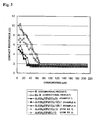
- Table 2 indicates the measurement results of the contact counts until the contact resistance exceeded 5 ⁇ .
- the pressing amounts (overdrive amount) of the probe pin on an aluminum pad from the start of the measurement until stabilization of the contact resistance in the above-described contamination resistance property evaluation were studied.
- Fig. 3 illustrates the measurement results of electrical contact properties.
- the probe pin including the material according to each of the examples exhibits an overdrive amount that is approximately half compared to a probe pin including tungsten, which is a conventional material, or a material according to each of the comparative examples, and thus, have a stable contact resistance. Accordingly, it was confirmed that they have a high electrical contact stability.
- the probe pin material according to the present invention has a high hardness and a low specific resistance, and is excellent in conductivity. Also, it includes precious metals as its main components, and thus, also has an excellent oxidation resistance.
- the present invention enables provision of probe pins that can be used stably for a long time and will not contaminate a test target.
Landscapes
- Chemical & Material Sciences (AREA)
- Engineering & Computer Science (AREA)
- Materials Engineering (AREA)
- Mechanical Engineering (AREA)
- Metallurgy (AREA)
- Organic Chemistry (AREA)
- Physics & Mathematics (AREA)
- General Physics & Mathematics (AREA)
- Thermal Sciences (AREA)
- Crystallography & Structural Chemistry (AREA)
- Measuring Leads Or Probes (AREA)
- Testing Or Measuring Of Semiconductors Or The Like (AREA)
Claims (2)
- Prozess zur Herstellung einer Sondenspitze aus einem Sondenspitzenmaterial, das aus Au, Ag, Pd und Cu und optional 0,6 bis 5 Gew.-% von zumindest einem Element besteht, das aus Ni, Zn und Co selektiert wurde, wobei das Material eine Härte von 300 bis 450 HV aufweist und durch Erhitzen einer Legierung mit einer Au-Konzentration von 40 bis 55 Gew.-%, einer Ag-Konzentration von 15 bis 30 Gew.-% und einer gesamten Pd- und Cu-Konzentration von 15 bis 40 Gew.-% bei einer Temperatur im Bereich 300 bis 500 °C gebildet wird, um die Legierung mittels Ausscheidungshärtung zu härten.
- Verfahren zum Testen der elektrischen Eigenschaften von halbleiterintegrierten Schaltkreiselementen oder Flüssigkristallanzeigegeräten, wobei Sondenspitzen auf einer Sondenkarte wiederholt mit den Elektrodenkontaktstellen solcher Elemente oder Geräte kontaktiert werden, dadurch gekennzeichnet, dass die Sondenspitzen ein Material, wie in Anspruch 1 definiert, umfassen.
Applications Claiming Priority (2)
| Application Number | Priority Date | Filing Date | Title |
|---|---|---|---|
| JP2007150737A JP4176133B1 (ja) | 2007-06-06 | 2007-06-06 | プローブピン |
| PCT/JP2008/060268 WO2008149886A1 (ja) | 2007-06-06 | 2008-06-04 | プローブピン用材料 |
Publications (3)
| Publication Number | Publication Date |
|---|---|
| EP2159581A1 EP2159581A1 (de) | 2010-03-03 |
| EP2159581A4 EP2159581A4 (de) | 2011-06-29 |
| EP2159581B1 true EP2159581B1 (de) | 2012-10-31 |
Family
ID=40056068
Family Applications (1)
| Application Number | Title | Priority Date | Filing Date |
|---|---|---|---|
| EP08765081A Not-in-force EP2159581B1 (de) | 2007-06-06 | 2008-06-04 | Verfahren zur Herstellung von Sondenspitzen |
Country Status (7)
| Country | Link |
|---|---|
| US (1) | US8310254B2 (de) |
| EP (1) | EP2159581B1 (de) |
| JP (1) | JP4176133B1 (de) |
| KR (1) | KR101323027B1 (de) |
| CN (1) | CN101715559B (de) |
| TW (1) | TWI375801B (de) |
| WO (1) | WO2008149886A1 (de) |
Families Citing this family (16)
| Publication number | Priority date | Publication date | Assignee | Title |
|---|---|---|---|---|
| JP4801757B2 (ja) * | 2009-05-29 | 2011-10-26 | 田中貴金属工業株式会社 | 接触抵抗、防汚特性に優れるプローブピン |
| JP2011158329A (ja) * | 2010-01-29 | 2011-08-18 | Citizen Tohoku Kk | コンタクトプローブ及びこれを用いた電子回路試験装置 |
| CN103249852A (zh) * | 2010-12-09 | 2013-08-14 | 株式会社德力本店 | 电气/电子材料 |
| JP4878401B1 (ja) * | 2011-05-17 | 2012-02-15 | 石福金属興業株式会社 | プローブピン用材料、プローブピン及びその製造方法 |
| JP2013101043A (ja) * | 2011-11-08 | 2013-05-23 | Renesas Electronics Corp | 半導体装置の製造方法 |
| EP2881479B1 (de) | 2012-08-03 | 2017-10-04 | Yamamoto Precious Metal Co., Ltd. | Legierungsmaterial, kontaktsonde und verbindungsklemme |
| WO2014049874A1 (ja) * | 2012-09-28 | 2014-04-03 | 株式会社徳力本店 | 電気・電子機器用途のAg‐Pd‐Cu‐Co合金 |
| MY190360A (en) | 2012-11-30 | 2022-04-17 | Honda Motor Co Ltd | Additional light structure of projector light assembly for motorcycle |
| JP6372952B2 (ja) * | 2013-10-25 | 2018-08-15 | 石福金属興業株式会社 | Pt基合金で構成されるプローブピン用材料、プローブピンの製造方法 |
| JPWO2019013163A1 (ja) * | 2017-07-10 | 2020-02-06 | 株式会社協成 | 銅銀合金を用いた導電性部材、コンタクトピン及び装置 |
| JP6850365B2 (ja) * | 2017-12-27 | 2021-03-31 | 株式会社徳力本店 | 析出硬化型Ag−Pd−Cu−In−B系合金 |
| JP7072126B1 (ja) | 2022-02-10 | 2022-05-19 | 田中貴金属工業株式会社 | Ag-Pd-Cu系合金からなるプローブピン用材料 |
| EP4325227B1 (de) * | 2022-08-16 | 2025-10-01 | Heraeus Precious Metals GmbH & Co. KG | Bandförmiger verbundwerkstoff für prüfnadeln |
| CN115792317A (zh) * | 2022-11-25 | 2023-03-14 | 卢世雄 | 一种用于检测半导体芯片的新型铍铜合金探针 |
| CN117310234B (zh) * | 2023-11-30 | 2024-03-01 | 浙江金连接科技股份有限公司 | 一种半导体芯片测试用钯合金探针套筒及其制造方法 |
| KR102934049B1 (ko) * | 2024-02-21 | 2026-03-05 | 하이콘 주식회사 | 석출경화 공정을 이용한 스프링 콘택트 핀의 제조 방법 |
Family Cites Families (15)
| Publication number | Priority date | Publication date | Assignee | Title |
|---|---|---|---|---|
| US3767391A (en) | 1969-05-19 | 1973-10-23 | Pennwalt Corp | Tarnish resistant alloy |
| SE368050B (de) | 1972-08-25 | 1974-06-17 | Electrolux Ab | |
| US5378971A (en) * | 1990-11-30 | 1995-01-03 | Tokyo Electron Limited | Probe and a method of manufacturing the same |
| JPH05154719A (ja) * | 1991-11-29 | 1993-06-22 | Tanaka Kikinzoku Kogyo Kk | プローブピンの製造装置 |
| JP3090389B2 (ja) * | 1993-11-24 | 2000-09-18 | 田中貴金属工業株式会社 | マルチワイヤープローブの製造方法 |
| JPH1038922A (ja) | 1996-07-26 | 1998-02-13 | Iwaki Electron Corp Ltd | プローブピン装置 |
| US5919320A (en) * | 1997-11-17 | 1999-07-06 | Leach & Garner Company | Nickel-free white gold alloy with reversible hardness characteristics |
| CN1073637C (zh) * | 1998-03-04 | 2001-10-24 | 贵研铂业股份有限公司 | 电接触材料金基合金 |
| US6517955B1 (en) * | 1999-02-22 | 2003-02-11 | Nippon Steel Corporation | High strength galvanized steel plate excellent in adhesion of plated metal and formability in press working and high strength alloy galvanized steel plate and method for production thereof |
| KR100745104B1 (ko) * | 2000-06-16 | 2007-08-01 | 니혼 하츠쵸 가부시키가이샤 | 컨택터 프로브, 전기 프로브 유닛, 컨택터 프로브를 위한 프로브 어셈블리와 절연체의 조합체 및 컨택터 프로브를 위한 탄성의 도전성 프로브 어셈블리 |
| EP1435398B1 (de) * | 2001-10-09 | 2007-11-28 | Kabushiki Kaisha Toshiba | Wolframdraht, kathodenheizer und glühfaden für lampe zur verwendung unter vibrationen |
| JP2004093355A (ja) | 2002-08-30 | 2004-03-25 | Toshiba Corp | Pd合金系プローブピンおよびそれを用いたプローブピン装置 |
| JP2004179327A (ja) * | 2002-11-26 | 2004-06-24 | Sharp Corp | 半導体用合金材料、該合金材料を用いた半導体チップ及びその製造方法 |
| US7135078B1 (en) * | 2005-12-05 | 2006-11-14 | Leach & Garner Company | Nickel-free white gold alloy compositions with reversible hardness characteristics |
| JP4946208B2 (ja) | 2006-06-29 | 2012-06-06 | 日本電産株式会社 | 記録媒体の保持装置とそれを用いたモータユニット |
-
2007
- 2007-06-06 JP JP2007150737A patent/JP4176133B1/ja not_active Expired - Fee Related
-
2008
- 2008-06-04 US US12/602,899 patent/US8310254B2/en not_active Expired - Fee Related
- 2008-06-04 CN CN2008800191603A patent/CN101715559B/zh not_active Expired - Fee Related
- 2008-06-04 EP EP08765081A patent/EP2159581B1/de not_active Not-in-force
- 2008-06-04 KR KR1020097025628A patent/KR101323027B1/ko not_active Expired - Fee Related
- 2008-06-04 WO PCT/JP2008/060268 patent/WO2008149886A1/ja not_active Ceased
- 2008-06-05 TW TW097120907A patent/TWI375801B/zh not_active IP Right Cessation
Also Published As
| Publication number | Publication date |
|---|---|
| KR101323027B1 (ko) | 2013-10-29 |
| CN101715559B (zh) | 2012-09-26 |
| US8310254B2 (en) | 2012-11-13 |
| TW200916788A (en) | 2009-04-16 |
| EP2159581A4 (de) | 2011-06-29 |
| CN101715559A (zh) | 2010-05-26 |
| KR20100010506A (ko) | 2010-02-01 |
| US20100176833A1 (en) | 2010-07-15 |
| JP4176133B1 (ja) | 2008-11-05 |
| EP2159581A1 (de) | 2010-03-03 |
| WO2008149886A1 (ja) | 2008-12-11 |
| TWI375801B (en) | 2012-11-01 |
| JP2008304266A (ja) | 2008-12-18 |
Similar Documents
| Publication | Publication Date | Title |
|---|---|---|
| EP2159581B1 (de) | Verfahren zur Herstellung von Sondenspitzen | |
| KR100718577B1 (ko) | 프로브 핀용 재료 | |
| EP4227426B1 (de) | Sondenstiftmaterial mit ag-pd-cu-basierter legierung | |
| JP7766290B2 (ja) | プローブピン用合金材料 | |
| JP6074244B2 (ja) | Ag基合金からなるプローブピン用材料、プローブピン、プローブピンの製造方法 | |
| JP7141098B2 (ja) | プローブピン用材料およびプローブピン | |
| JP6850365B2 (ja) | 析出硬化型Ag−Pd−Cu−In−B系合金 | |
| KR101260135B1 (ko) | 접촉저항, 방오특성이 우수한 프로브 핀 | |
| JP2021080552A (ja) | プローブピン用材料およびプローブピン | |
| JP7798263B2 (ja) | プローブピン用合金材料 | |
| KR20250053083A (ko) | 프로브 핀용 합금 재료 | |
| JP7429011B2 (ja) | プローブピン用材料およびプローブピン | |
| EP4317491A1 (de) | Legierungsmaterial für sondenspitzen | |
| JP2024089037A (ja) | プローブピン用合金材料 | |
| CN117015625A (zh) | 探测针用合金材料 |
Legal Events
| Date | Code | Title | Description |
|---|---|---|---|
| PUAI | Public reference made under article 153(3) epc to a published international application that has entered the european phase |
Free format text: ORIGINAL CODE: 0009012 |
|
| 17P | Request for examination filed |
Effective date: 20100106 |
|
| AK | Designated contracting states |
Kind code of ref document: A1 Designated state(s): AT BE BG CH CY CZ DE DK EE ES FI FR GB GR HR HU IE IS IT LI LT LU LV MC MT NL NO PL PT RO SE SI SK TR |
|
| AX | Request for extension of the european patent |
Extension state: AL BA MK RS |
|
| DAX | Request for extension of the european patent (deleted) | ||
| A4 | Supplementary search report drawn up and despatched |
Effective date: 20110530 |
|
| 17Q | First examination report despatched |
Effective date: 20120120 |
|
| GRAP | Despatch of communication of intention to grant a patent |
Free format text: ORIGINAL CODE: EPIDOSNIGR1 |
|
| GRAS | Grant fee paid |
Free format text: ORIGINAL CODE: EPIDOSNIGR3 |
|
| GRAA | (expected) grant |
Free format text: ORIGINAL CODE: 0009210 |
|
| AK | Designated contracting states |
Kind code of ref document: B1 Designated state(s): AT BE BG CH CY CZ DE DK EE ES FI FR GB GR HR HU IE IS IT LI LT LU LV MC MT NL NO PL PT RO SE SI SK TR |
|
| REG | Reference to a national code |
Ref country code: GB Ref legal event code: FG4D Ref country code: CH Ref legal event code: EP |
|
| REG | Reference to a national code |
Ref country code: AT Ref legal event code: REF Ref document number: 582287 Country of ref document: AT Kind code of ref document: T Effective date: 20121115 |
|
| REG | Reference to a national code |
Ref country code: IE Ref legal event code: FG4D |
|
| REG | Reference to a national code |
Ref country code: DE Ref legal event code: R096 Ref document number: 602008019814 Country of ref document: DE Effective date: 20121227 |
|
| REG | Reference to a national code |
Ref country code: AT Ref legal event code: MK05 Ref document number: 582287 Country of ref document: AT Kind code of ref document: T Effective date: 20121031 |
|
| REG | Reference to a national code |
Ref country code: LT Ref legal event code: MG4D |
|
| REG | Reference to a national code |
Ref country code: NL Ref legal event code: VDEP Effective date: 20121031 |
|
| PG25 | Lapsed in a contracting state [announced via postgrant information from national office to epo] |
Ref country code: SE Free format text: LAPSE BECAUSE OF FAILURE TO SUBMIT A TRANSLATION OF THE DESCRIPTION OR TO PAY THE FEE WITHIN THE PRESCRIBED TIME-LIMIT Effective date: 20121031 Ref country code: NO Free format text: LAPSE BECAUSE OF FAILURE TO SUBMIT A TRANSLATION OF THE DESCRIPTION OR TO PAY THE FEE WITHIN THE PRESCRIBED TIME-LIMIT Effective date: 20130131 Ref country code: NL Free format text: LAPSE BECAUSE OF FAILURE TO SUBMIT A TRANSLATION OF THE DESCRIPTION OR TO PAY THE FEE WITHIN THE PRESCRIBED TIME-LIMIT Effective date: 20121031 Ref country code: IS Free format text: LAPSE BECAUSE OF FAILURE TO SUBMIT A TRANSLATION OF THE DESCRIPTION OR TO PAY THE FEE WITHIN THE PRESCRIBED TIME-LIMIT Effective date: 20130228 Ref country code: LT Free format text: LAPSE BECAUSE OF FAILURE TO SUBMIT A TRANSLATION OF THE DESCRIPTION OR TO PAY THE FEE WITHIN THE PRESCRIBED TIME-LIMIT Effective date: 20121031 Ref country code: HR Free format text: LAPSE BECAUSE OF FAILURE TO SUBMIT A TRANSLATION OF THE DESCRIPTION OR TO PAY THE FEE WITHIN THE PRESCRIBED TIME-LIMIT Effective date: 20121031 Ref country code: FI Free format text: LAPSE BECAUSE OF FAILURE TO SUBMIT A TRANSLATION OF THE DESCRIPTION OR TO PAY THE FEE WITHIN THE PRESCRIBED TIME-LIMIT Effective date: 20121031 Ref country code: ES Free format text: LAPSE BECAUSE OF FAILURE TO SUBMIT A TRANSLATION OF THE DESCRIPTION OR TO PAY THE FEE WITHIN THE PRESCRIBED TIME-LIMIT Effective date: 20130211 |
|
| PG25 | Lapsed in a contracting state [announced via postgrant information from national office to epo] |
Ref country code: SI Free format text: LAPSE BECAUSE OF FAILURE TO SUBMIT A TRANSLATION OF THE DESCRIPTION OR TO PAY THE FEE WITHIN THE PRESCRIBED TIME-LIMIT Effective date: 20121031 Ref country code: PL Free format text: LAPSE BECAUSE OF FAILURE TO SUBMIT A TRANSLATION OF THE DESCRIPTION OR TO PAY THE FEE WITHIN THE PRESCRIBED TIME-LIMIT Effective date: 20121031 Ref country code: BE Free format text: LAPSE BECAUSE OF FAILURE TO SUBMIT A TRANSLATION OF THE DESCRIPTION OR TO PAY THE FEE WITHIN THE PRESCRIBED TIME-LIMIT Effective date: 20121031 Ref country code: PT Free format text: LAPSE BECAUSE OF FAILURE TO SUBMIT A TRANSLATION OF THE DESCRIPTION OR TO PAY THE FEE WITHIN THE PRESCRIBED TIME-LIMIT Effective date: 20130228 Ref country code: GR Free format text: LAPSE BECAUSE OF FAILURE TO SUBMIT A TRANSLATION OF THE DESCRIPTION OR TO PAY THE FEE WITHIN THE PRESCRIBED TIME-LIMIT Effective date: 20130201 Ref country code: LV Free format text: LAPSE BECAUSE OF FAILURE TO SUBMIT A TRANSLATION OF THE DESCRIPTION OR TO PAY THE FEE WITHIN THE PRESCRIBED TIME-LIMIT Effective date: 20121031 |
|
| PG25 | Lapsed in a contracting state [announced via postgrant information from national office to epo] |
Ref country code: AT Free format text: LAPSE BECAUSE OF FAILURE TO SUBMIT A TRANSLATION OF THE DESCRIPTION OR TO PAY THE FEE WITHIN THE PRESCRIBED TIME-LIMIT Effective date: 20121031 |
|
| PG25 | Lapsed in a contracting state [announced via postgrant information from national office to epo] |
Ref country code: CZ Free format text: LAPSE BECAUSE OF FAILURE TO SUBMIT A TRANSLATION OF THE DESCRIPTION OR TO PAY THE FEE WITHIN THE PRESCRIBED TIME-LIMIT Effective date: 20121031 Ref country code: EE Free format text: LAPSE BECAUSE OF FAILURE TO SUBMIT A TRANSLATION OF THE DESCRIPTION OR TO PAY THE FEE WITHIN THE PRESCRIBED TIME-LIMIT Effective date: 20121031 Ref country code: BG Free format text: LAPSE BECAUSE OF FAILURE TO SUBMIT A TRANSLATION OF THE DESCRIPTION OR TO PAY THE FEE WITHIN THE PRESCRIBED TIME-LIMIT Effective date: 20130131 Ref country code: DK Free format text: LAPSE BECAUSE OF FAILURE TO SUBMIT A TRANSLATION OF THE DESCRIPTION OR TO PAY THE FEE WITHIN THE PRESCRIBED TIME-LIMIT Effective date: 20121031 Ref country code: SK Free format text: LAPSE BECAUSE OF FAILURE TO SUBMIT A TRANSLATION OF THE DESCRIPTION OR TO PAY THE FEE WITHIN THE PRESCRIBED TIME-LIMIT Effective date: 20121031 |
|
| PG25 | Lapsed in a contracting state [announced via postgrant information from national office to epo] |
Ref country code: IT Free format text: LAPSE BECAUSE OF FAILURE TO SUBMIT A TRANSLATION OF THE DESCRIPTION OR TO PAY THE FEE WITHIN THE PRESCRIBED TIME-LIMIT Effective date: 20121031 Ref country code: RO Free format text: LAPSE BECAUSE OF FAILURE TO SUBMIT A TRANSLATION OF THE DESCRIPTION OR TO PAY THE FEE WITHIN THE PRESCRIBED TIME-LIMIT Effective date: 20121031 |
|
| PLBE | No opposition filed within time limit |
Free format text: ORIGINAL CODE: 0009261 |
|
| STAA | Information on the status of an ep patent application or granted ep patent |
Free format text: STATUS: NO OPPOSITION FILED WITHIN TIME LIMIT |
|
| 26N | No opposition filed |
Effective date: 20130801 |
|
| REG | Reference to a national code |
Ref country code: DE Ref legal event code: R097 Ref document number: 602008019814 Country of ref document: DE Effective date: 20130801 |
|
| PG25 | Lapsed in a contracting state [announced via postgrant information from national office to epo] |
Ref country code: CY Free format text: LAPSE BECAUSE OF FAILURE TO SUBMIT A TRANSLATION OF THE DESCRIPTION OR TO PAY THE FEE WITHIN THE PRESCRIBED TIME-LIMIT Effective date: 20121031 |
|
| PG25 | Lapsed in a contracting state [announced via postgrant information from national office to epo] |
Ref country code: MC Free format text: LAPSE BECAUSE OF FAILURE TO SUBMIT A TRANSLATION OF THE DESCRIPTION OR TO PAY THE FEE WITHIN THE PRESCRIBED TIME-LIMIT Effective date: 20121031 |
|
| REG | Reference to a national code |
Ref country code: CH Ref legal event code: PL |
|
| REG | Reference to a national code |
Ref country code: IE Ref legal event code: MM4A |
|
| PG25 | Lapsed in a contracting state [announced via postgrant information from national office to epo] |
Ref country code: CH Free format text: LAPSE BECAUSE OF NON-PAYMENT OF DUE FEES Effective date: 20130630 Ref country code: IE Free format text: LAPSE BECAUSE OF NON-PAYMENT OF DUE FEES Effective date: 20130604 Ref country code: LI Free format text: LAPSE BECAUSE OF NON-PAYMENT OF DUE FEES Effective date: 20130630 |
|
| PG25 | Lapsed in a contracting state [announced via postgrant information from national office to epo] |
Ref country code: MT Free format text: LAPSE BECAUSE OF FAILURE TO SUBMIT A TRANSLATION OF THE DESCRIPTION OR TO PAY THE FEE WITHIN THE PRESCRIBED TIME-LIMIT Effective date: 20121031 |
|
| PG25 | Lapsed in a contracting state [announced via postgrant information from national office to epo] |
Ref country code: TR Free format text: LAPSE BECAUSE OF FAILURE TO SUBMIT A TRANSLATION OF THE DESCRIPTION OR TO PAY THE FEE WITHIN THE PRESCRIBED TIME-LIMIT Effective date: 20121031 |
|
| PG25 | Lapsed in a contracting state [announced via postgrant information from national office to epo] |
Ref country code: LU Free format text: LAPSE BECAUSE OF NON-PAYMENT OF DUE FEES Effective date: 20130604 Ref country code: HU Free format text: LAPSE BECAUSE OF FAILURE TO SUBMIT A TRANSLATION OF THE DESCRIPTION OR TO PAY THE FEE WITHIN THE PRESCRIBED TIME-LIMIT; INVALID AB INITIO Effective date: 20080604 |
|
| REG | Reference to a national code |
Ref country code: FR Ref legal event code: PLFP Year of fee payment: 9 |
|
| REG | Reference to a national code |
Ref country code: FR Ref legal event code: PLFP Year of fee payment: 10 |
|
| REG | Reference to a national code |
Ref country code: FR Ref legal event code: PLFP Year of fee payment: 11 |
|
| PGFP | Annual fee paid to national office [announced via postgrant information from national office to epo] |
Ref country code: FR Payment date: 20210622 Year of fee payment: 14 |
|
| PGFP | Annual fee paid to national office [announced via postgrant information from national office to epo] |
Ref country code: GB Payment date: 20210625 Year of fee payment: 14 |
|
| PGFP | Annual fee paid to national office [announced via postgrant information from national office to epo] |
Ref country code: DE Payment date: 20220620 Year of fee payment: 15 |
|
| GBPC | Gb: european patent ceased through non-payment of renewal fee |
Effective date: 20220604 |
|
| PG25 | Lapsed in a contracting state [announced via postgrant information from national office to epo] |
Ref country code: FR Free format text: LAPSE BECAUSE OF NON-PAYMENT OF DUE FEES Effective date: 20220630 |
|
| PG25 | Lapsed in a contracting state [announced via postgrant information from national office to epo] |
Ref country code: GB Free format text: LAPSE BECAUSE OF NON-PAYMENT OF DUE FEES Effective date: 20220604 |
|
| REG | Reference to a national code |
Ref country code: DE Ref legal event code: R119 Ref document number: 602008019814 Country of ref document: DE |
|
| PG25 | Lapsed in a contracting state [announced via postgrant information from national office to epo] |
Ref country code: DE Free format text: LAPSE BECAUSE OF NON-PAYMENT OF DUE FEES Effective date: 20240103 |