EP2159648B1 - Verfahren zum Aufladen von Toner zur Elektrofotografie unter Verwendung von Kohlenstoffnanoröhrchen oder anderen Nanostrukturen - Google Patents
Verfahren zum Aufladen von Toner zur Elektrofotografie unter Verwendung von Kohlenstoffnanoröhrchen oder anderen Nanostrukturen Download PDFInfo
- Publication number
- EP2159648B1 EP2159648B1 EP09167683.3A EP09167683A EP2159648B1 EP 2159648 B1 EP2159648 B1 EP 2159648B1 EP 09167683 A EP09167683 A EP 09167683A EP 2159648 B1 EP2159648 B1 EP 2159648B1
- Authority
- EP
- European Patent Office
- Prior art keywords
- electrode
- electric field
- nanostructures
- array
- particles
- Prior art date
- Legal status (The legal status is an assumption and is not a legal conclusion. Google has not performed a legal analysis and makes no representation as to the accuracy of the status listed.)
- Not-in-force
Links
- 239000002086 nanomaterial Substances 0.000 title claims description 45
- 238000000034 method Methods 0.000 title claims description 29
- OKTJSMMVPCPJKN-UHFFFAOYSA-N Carbon Chemical compound [C] OKTJSMMVPCPJKN-UHFFFAOYSA-N 0.000 title description 3
- 239000002041 carbon nanotube Substances 0.000 title description 2
- 229910021393 carbon nanotube Inorganic materials 0.000 title description 2
- 239000002245 particle Substances 0.000 claims description 76
- 230000005684 electric field Effects 0.000 claims description 50
- 239000000758 substrate Substances 0.000 claims description 20
- 238000003491 array Methods 0.000 claims description 4
- 239000011248 coating agent Substances 0.000 description 3
- 238000000576 coating method Methods 0.000 description 3
- 230000001681 protective effect Effects 0.000 description 3
- RYGMFSIKBFXOCR-UHFFFAOYSA-N Copper Chemical compound [Cu] RYGMFSIKBFXOCR-UHFFFAOYSA-N 0.000 description 2
- 229910052802 copper Inorganic materials 0.000 description 2
- 239000010949 copper Substances 0.000 description 2
- 239000002079 double walled nanotube Substances 0.000 description 2
- 239000000463 material Substances 0.000 description 2
- VNWKTOKETHGBQD-UHFFFAOYSA-N methane Chemical compound C VNWKTOKETHGBQD-UHFFFAOYSA-N 0.000 description 2
- 229920001721 polyimide Polymers 0.000 description 2
- 239000002109 single walled nanotube Substances 0.000 description 2
- 239000004642 Polyimide Substances 0.000 description 1
- 239000004793 Polystyrene Substances 0.000 description 1
- 239000000654 additive Substances 0.000 description 1
- 239000011365 complex material Substances 0.000 description 1
- 239000004020 conductor Substances 0.000 description 1
- 230000001276 controlling effect Effects 0.000 description 1
- 238000011161 development Methods 0.000 description 1
- 238000001914 filtration Methods 0.000 description 1
- PCHJSUWPFVWCPO-UHFFFAOYSA-N gold Chemical compound [Au] PCHJSUWPFVWCPO-UHFFFAOYSA-N 0.000 description 1
- 229910052737 gold Inorganic materials 0.000 description 1
- 239000010931 gold Substances 0.000 description 1
- 239000002184 metal Substances 0.000 description 1
- 229910052751 metal Inorganic materials 0.000 description 1
- 238000001465 metallisation Methods 0.000 description 1
- 239000000615 nonconductor Substances 0.000 description 1
- 229920000728 polyester Polymers 0.000 description 1
- 229920002223 polystyrene Polymers 0.000 description 1
- 239000000843 powder Substances 0.000 description 1
- 230000001105 regulatory effect Effects 0.000 description 1
- 238000011160 research Methods 0.000 description 1
- 230000003068 static effect Effects 0.000 description 1
- 238000001771 vacuum deposition Methods 0.000 description 1
- XLYOFNOQVPJJNP-UHFFFAOYSA-N water Substances O XLYOFNOQVPJJNP-UHFFFAOYSA-N 0.000 description 1
Images


Classifications
-
- G—PHYSICS
- G03—PHOTOGRAPHY; CINEMATOGRAPHY; ANALOGOUS TECHNIQUES USING WAVES OTHER THAN OPTICAL WAVES; ELECTROGRAPHY; HOLOGRAPHY
- G03G—ELECTROGRAPHY; ELECTROPHOTOGRAPHY; MAGNETOGRAPHY
- G03G15/00—Apparatus for electrographic processes using a charge pattern
- G03G15/02—Apparatus for electrographic processes using a charge pattern for laying down a uniform charge, e.g. for sensitising; Corona discharge devices
- G03G15/0291—Apparatus for electrographic processes using a charge pattern for laying down a uniform charge, e.g. for sensitising; Corona discharge devices corona discharge devices, e.g. wires, pointed electrodes, means for cleaning the corona discharge device
-
- G—PHYSICS
- G03—PHOTOGRAPHY; CINEMATOGRAPHY; ANALOGOUS TECHNIQUES USING WAVES OTHER THAN OPTICAL WAVES; ELECTROGRAPHY; HOLOGRAPHY
- G03G—ELECTROGRAPHY; ELECTROPHOTOGRAPHY; MAGNETOGRAPHY
- G03G15/00—Apparatus for electrographic processes using a charge pattern
- G03G15/06—Apparatus for electrographic processes using a charge pattern for developing
- G03G15/08—Apparatus for electrographic processes using a charge pattern for developing using a solid developer, e.g. powder developer
-
- G—PHYSICS
- G03—PHOTOGRAPHY; CINEMATOGRAPHY; ANALOGOUS TECHNIQUES USING WAVES OTHER THAN OPTICAL WAVES; ELECTROGRAPHY; HOLOGRAPHY
- G03G—ELECTROGRAPHY; ELECTROPHOTOGRAPHY; MAGNETOGRAPHY
- G03G15/00—Apparatus for electrographic processes using a charge pattern
- G03G15/02—Apparatus for electrographic processes using a charge pattern for laying down a uniform charge, e.g. for sensitising; Corona discharge devices
-
- G—PHYSICS
- G03—PHOTOGRAPHY; CINEMATOGRAPHY; ANALOGOUS TECHNIQUES USING WAVES OTHER THAN OPTICAL WAVES; ELECTROGRAPHY; HOLOGRAPHY
- G03G—ELECTROGRAPHY; ELECTROPHOTOGRAPHY; MAGNETOGRAPHY
- G03G15/00—Apparatus for electrographic processes using a charge pattern
- G03G15/06—Apparatus for electrographic processes using a charge pattern for developing
- G03G15/08—Apparatus for electrographic processes using a charge pattern for developing using a solid developer, e.g. powder developer
- G03G15/0822—Arrangements for preparing, mixing, supplying or dispensing developer
-
- G—PHYSICS
- G03—PHOTOGRAPHY; CINEMATOGRAPHY; ANALOGOUS TECHNIQUES USING WAVES OTHER THAN OPTICAL WAVES; ELECTROGRAPHY; HOLOGRAPHY
- G03G—ELECTROGRAPHY; ELECTROPHOTOGRAPHY; MAGNETOGRAPHY
- G03G2215/00—Apparatus for electrophotographic processes
- G03G2215/06—Developing structures, details
- G03G2215/0602—Developer
- G03G2215/0604—Developer solid type
- G03G2215/0614—Developer solid type one-component
- G03G2215/0619—Developer solid type one-component non-contact (flying development)
-
- G—PHYSICS
- G03—PHOTOGRAPHY; CINEMATOGRAPHY; ANALOGOUS TECHNIQUES USING WAVES OTHER THAN OPTICAL WAVES; ELECTROGRAPHY; HOLOGRAPHY
- G03G—ELECTROGRAPHY; ELECTROPHOTOGRAPHY; MAGNETOGRAPHY
- G03G2215/00—Apparatus for electrophotographic processes
- G03G2215/06—Developing structures, details
- G03G2215/0634—Developing device
- G03G2215/0636—Specific type of dry developer device
- G03G2215/0641—Without separate supplying member (i.e. with developing housing sliding on donor member)
Definitions
- the present invention relates to image forming apparatus and more particularly to systems and methods of charging particles.
- US-A-2006/0210316 describes a system for providing charged particles in which a string of particles is subjected to electron bondardment while being blown along a passage extending between carbon nanotubes.
- US-A-2002/0037102 discloses an image forming apparatus including a toner flying device for electrostatically conveying toner along a conveying surface using electric field extending between opposed arrays of electrodes.
- US-A-5893015 describes another example of apparatus for transporting charged particles using a donor member.
- the donor member includes an electric array on its surface including a plurality of spaced apart electrodes.
- US-A-2007/0235647 discloses electrophotographic charging devices that can be used to charge or discharge, for example, a receptor in the electrophotographic process are provided.
- the exemplary charging devices can include a coronode disposed opposing and spaced apart from a receptor, and a plurality of nanostructures, wherein each of the plurality of nanostructures has an end, edge, or side in electrical contact with the coronode.
- a method to impart an electrostatic charge to particles comprises providing a plurality of particles to be charged; and providing a plurality of nanostructures disposed over a first electrode, the first electrode disposed in close proximity to a rotating surface; characterised in that the particles are toner particles; and in that the method further comprises applying an electric field between the first electrode and the rotating surface, thereby causing electron emission from the plurality of nanostructures and charging a plurality of charged toner particles between the first electrode and the rotating surface.
- the method can also include providing a multi-phase voltage source operatively coupled to the first electrode array and applying a multi-phase voltage to the first electrode array to create a traveling electric field between each electrode of the first electrode array, thereby causing electron emission from the plurality of nanostructures and forming a plurality of charged toner particles.
- the method can further include transporting each of the plurality of charged toner particles using the traveling electric field onto a surface.
- a system to impart an electrostatic charge to particles comprises a plurality of particles to be charged; and a plurality of nanostructures disposed over a first electrode, the first electrode disposed in close proximity to a rotating surface; characterized in that the particles are toner particles; and in that the system further comprises a power source operatively coupled between the first electrode and the surface to supply a voltage to create an electric field between the first electrode and the rotating surface, wherein the electric field causes an electron emission from the plurality of nanostructures to form a plurality of charged particles.
- FIG. 1 illustrates an exemplary system 100 to impart an electrostatic charge to a particle 145.
- the system 100 can include a plurality of nanostructures 120 disposed over a first electrode array 111, wherein the first electrode array 111 can include a plurality of electrodes spaced apart, as shown in FIG. 1 .
- the plurality of nanostructures 120 can be disposed over a first substrate 110, the first substrate 110 including the first electrode array 111.
- the first electrode array 111 can be deposited over an electrically insulating substrate 110 and coated over with a protective and charge dissipative coating (not shown) to get rid of the static charge build up.
- Exemplary materials for the substrate 110 can include, but are not limited to, polyimide, polyester, polystyrene, or any good electrical insulator.
- Exemplary material for the first electrode array 111 can include, copper, gold, or any good electrical conductor.
- Exemplary nanostructures 120 can include, but are not limited to single walled carbon nanotubes (SWNT), double walled carbon nanotubes (DWNT), and combinations thereof.
- SWNT single walled carbon nanotubes
- DWNT double walled carbon nanotubes
- nanostructures 120 can be formed of one or more elements from Groups IV, V, VI, VII VIII, IB, IIB, IVA and VA.
- the nanostructures 120 can be fabricated by any suitable method, including, but not limited to, vacuum metallization and vacuum deposition.
- the nanostructures 120 can have a diameter from about 10 nm to about 450 nm and length from about 1 ⁇ m to about 200 ⁇ m.
- the system 100 can also include a power source 130 operatively coupled to the first electrode array 111 to supply a multi-phase voltage to the first electrode array 111 to create a traveling electric field between each electrode of the first electrode array 111, wherein the traveling electric field can cause an electron emission from the plurality of nanostructures 120 and form a plurality of charged particles 146.
- an amount of electrostatic charge of each of the plurality of charged particles 146 can be controlled by the magnitude and frequency of the traveling electric field.
- the system 100 can also include a surface 150 in close proximity to the plurality of nanostructures 120, wherein the plurality of charged particles 146 can be transported onto the surface 150 using the traveling electric field.
- the surface 150 can include at least one of a donor roll, a belt, a receptor, and a semi-conductive substrate. In certain embodiments, the surface 150 can include a rotating substrate. In some embodiments, the power source 130 can be operatively coupled to the first electrode array 111 and the surface150.
- FIG. 2 shows another exemplary system 200 to impart an electrostatic charge to particles 245.
- the system 200 can include a first plurality of nanostructures 220 disposed over a first electrode array 211, the first electrode array 211 including a plurality of electrodes spaced apart and a second plurality of nanostructures 220' disposed over a second electrode array 211', the second electrode array 211' including a plurality of electrodes spaced apart, wherein the second electrode array 211' can be disposed substantially parallel to and opposite to the first electrode array 211.
- the first plurality of nanostructures 220 can be disposed over a first substrate 210, the first substrate 210 including the first electrode array 211 and the second plurality of nanostructures 220' can be disposed over a second substrate 210', the second substrate 210' including the second electrode array 211'.
- the first electrode array 211 can be deposited over an electrically insulating substrate 210 and coated over with a protective and charge dissipative coating.
- the second electrode array 211' can be deposited over an electrically insulating substrate 210' and coated over with a protective and charge dissipative coating.
- the system 200 can also include a power source 230 operatively coupled to the first electrode array 211 and the second electrode array 211' to apply multi-phase voltages to the first electrode array 211 and the second electrode array 211' to create a traveling electric field between each electrode of the first and the second electrode array 211, 211'.
- the system 200 can also include a surface 250 in close proximity to the plurality of nanostructures 220, 220' wherein the plurality of charged particles 246 can be transported onto the surface 250 using the traveling electric field.
- the substrate 110, 210, 210' can be a flexible circuit board including about 20 ⁇ m to about 150 ⁇ m thick polyimide film having metal electrodes such as, copper.
- each of the plurality of electrodes of the first electrode array 111, 211 and the second electrode array 211' can have a width from about 10 ⁇ m to about 100 ⁇ m and a thickness from about 4 ⁇ m to about 10 ⁇ m.
- the first and the second electrode array 111, 211, 211' can have a spacing between each of the plurality of electrodes equal to the width of each of the plurality of electrodes.
- the method can include providing a plurality of particles 145, 245 to be charged, providing a plurality of nanostructures 120, 220 disposed over a first electrode array 111, 211, the first electrode array 111, 211 including a plurality of electrodes spaced apart, and providing a multi-phase voltage source 130, 230 operatively coupled to the first electrode array 211.
- the step of providing a multi-phase voltage source 130, 230 can include providing a multi-phase voltage source 130 operatively coupled to the first electrode array 111 and the surface 150 as shown in FIG. 1 .
- the step of providing a plurality of nanostructures 120, 220 disposed over a first electrode array 111, 211 can include providing a plurality of nanostructures 120, 220 disposed over the substrate 110, 210 including the first electrode array 111, 211.
- the method can also include applying a multi-phase voltage to the first electrode array 111, 211 to create a traveling electric field between each electrode of the first electrode array 111, 211, thereby causing an electron emission from the plurality of nanostructures 120, 220 and forming a plurality of charged particles 146, 246 and transporting each of the plurality of charged particles 146, 246 using the traveling electric field onto a surface150, 250.
- the method can further include using the frequency and magnitude of the traveling electric field to control an amount of electrostatic charge of each of the plurality of charged particles 146, 246.
- the method can further include providing a second plurality of nanostructures 220' disposed over a second electrode array 211', the second electrode array 211' including a plurality of electrodes spaced apart, wherein the second electrode array 211' can be disposed substantially parallel to and opposite to the first electrode array 211, as shown in FIG. 2 .
- the step of applying a multi-phase voltage to the first electrode array 211 to create a traveling electric field between each electrode of the first electrode array 211 can include applying multi-phase voltages to the first and the second electrode array 211, 211' to create traveling electric fields between each electrode of the first and the second electrode array.
- the electric field in the traveling electric field drops off as one move off the substrate 210 in a direction perpendicular to the active region.
- particle charging can occur in the regions where the fields are strongest and the transport field (traveling electric field) is also strongest here tending to move the charged particles along the substrate 210.
- the placement of the parallel traveling electric field grid allows particles 145, 245 which drift out of the transport fields of the first or the second electrode array 111, 211, 211' to be captured by the other.
- the traveling electric field can be at least one of a square-wave alternating electric field, a sinusoidal alternating electric field, and sum of sinusoidal electric fields, wherein the sum of sinusoidal electric fields would encompass any continuous waveform of the sort: f 2 ⁇ ⁇ ⁇ ⁇ x ⁇ 2 ⁇ ⁇ f ⁇ t .
- a traveling electric field can be created using two or more phases and one or more different waveforms.
- the method to impart an electrostatic charge to the particles 145, 245 can include filtering with respect to charge concurrently with the charging of the particles 145, 245 because the condition for particle 145, 245 travel is a function of the charge of the particle 145, 245, so the particle 145, 245 move out of the electrode area and onto the surface when the particle 145, 245 reaches an optimum charge and become charged particle 146, 246 as determined by the frequency and magnitude of the traveling electric field. Furthermore, the frequency and/or magnitude of the traveling electric field can be controlled to produce an optimum charge level of the particles 146, 246.
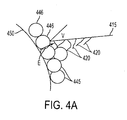
- the systems 300, 400 can include a plurality of particles 345, 445 to be charged and a plurality of nanostructures 320, 420 disposed over a first electrode 315, 415, wherein the first electrode 315, 415 can be disposed in close proximity to a rotating surface 350, 450.
- the systems 300, 400 can also include a power source 330, 430 to supply a voltage to create an electric field between the first electrode 315, 415 and the rotating surface 350, 450, wherein the electric field can cause an electron emission from the plurality of nanostructures 320, 420 and form a plurality of charged particles 346, 446.
- the plurality of particles 345 to be charged can be disposed over the plurality of nanostructures 320, as shown in FIG. 3 .
- the plurality of particles 445 to be charged can be disposed over the rotating surface 450, as shown in FIGS. 4 and 4A .
- the first electrode 415 can have a blade shape, as shown in FIGS. 4 and 4A .
- the rotating surface 350, 450 can include at least one of a donor roll, a belt, a receptor, and a semi-conductive substrate.
- the method can include providing a plurality of particles 345, 445 to be charged and providing a plurality of nanostructures 320, 420 disposed over a first electrode 315, 415, wherein the first electrode 315, 415 can be disposed in close proximity to a rotating surface 350, 450, as shown in FIGS. 3, 4 , and 4A .
- the step of providing a plurality of particles 345, 445 to be charged can include providing a plurality of particles 345 to be charged disposed over the plurality of nanostructures 320, as shown in FIG. 3 .
- the step of providing a plurality of particles 345, 445 to be charged can include providing a plurality of particles 445 to be charged disposed over the rotating surface 450, as shown in FIGS. 4 and 4A .
- the step of providing a plurality of nanostructures 420 disposed over a first electrode 415 can include providing a first electrode 415 having a blade shape, as shown in FIGS. 4 and 4A .
- the method can also include applying an electric field between the first electrode 315, 415 and the rotating surface 350, 450, thereby causing electron emission from the plurality of nanostructures 320, 420 and forming a plurality of charged particles 346, 446.
Landscapes
- Physics & Mathematics (AREA)
- General Physics & Mathematics (AREA)
- Engineering & Computer Science (AREA)
- Plasma & Fusion (AREA)
- Dry Development In Electrophotography (AREA)
- Electrostatic Spraying Apparatus (AREA)
- Printers Or Recording Devices Using Electromagnetic And Radiation Means (AREA)
- Physical Or Chemical Processes And Apparatus (AREA)
- Developing For Electrophotography (AREA)
- Elimination Of Static Electricity (AREA)
Claims (15)
- Verfahren zum Versehen von Partikeln mit einer elektrostatischen Ladung, umfassend:Vorsehen einer Vielzahl von Partikeln (145), die geladen werden sollen, undVorsehen einer Vielzahl von Nanostrukturen (120) über einer ersten Elektrode (111), wobei die erste Elektrode in nächster Nähe zu einer sich drehenden Fläche (150) angeordnet ist, dadurch gekennzeichnet, dass die Partikel Tonerpartikel (145) sind und das Verfahren weiterhin umfasst:Anlegen eines elektrischen Felds zwischen der ersten Elektrode (111) und der sich drehenden Fläche (150), um eine Elektronenemission von der Vielzahl von Nanostrukturen (120) zu veranlassen und eine Vielzahl von geladenen Tonerpartikeln zwischen der ersten Elektrode (111) und der sich drehenden Fläche (150) zu laden.
- Verfahren nach Anspruch 1, wobei der Schritt zum Vorsehen einer Vielzahl von Nanostrukturen (120) über einer ersten Elektrode das Vorsehen einer ersten Elektrode mit einer Klingenform (415) umfasst.
- Verfahren nach Anspruch 1, das weiterhin umfasst:Vorsehen der Vielzahl von Nanostrukturen (120) über einer Anordnung aus lateral beabstandeten ersten Elektroden (111),wobei das elektrische Feld durch eine Mehrphasen-Spannungsquelle (130) vorgesehen wird, die operativ mit den ersten Elektroden gekoppelt ist,Anlegen einer Mehrphasenspannung an der Anordnung von ersten Elektroden (111), um ein sich bewegendes elektrisches Feld zwischen den ersten Elektroden zu erzeugen, wobei die Mehrphasen-Spannungsquelle operativ mit der Elektrodenanordnung (111) und der Fläche (150) gekoppelt ist, um eine Elektronenemission von der Vielzahl von Nanostrukturen zu veranlassen und eine Vielzahl von geladenen Tonerpartikeln zu bilden, undTransportieren jeder aus der Vielzahl von geladenen Tonerpartikeln (145) unter Verwendung des sich bewegenden elektrischen Fels auf die Fläche (150).
- Verfahren nach Anspruch 3, das weiterhin das Verwenden der Frequenz und der Größe des sich bewegenden elektrischen Felds zum Steuern der Menge der elektrostatischen Ladung jedes aus der Vielzahl von geladenen Tonerpartikeln umfasst.
- Verfahren nach Anspruch 3 oder Anspruch 4, das weiterhin das Vorsehen einer zweiten Vielzahl von Nanostrukturen (220') über einer zweiten Elektrodenanordnung (211') umfasst, wobei die zweite Elektrodenanordnung eine Vielzahl von lateral beabstandeten Elektroden umfasst, wobei die zweite Elektrodenanordnung (211') im Wesentlichen parallel zu und gegenüber der einen Elektrodenanordnung (211) angeordnet ist.
- Verfahren nach Anspruch 5, wobei der Schritt zum Anlegen einer Mehrphasenspannung an der Anordnung der ersten Elektroden (211) zum Erzeugen eines sich bewegenden elektrischen Felds zwischen jeder ersten Elektrode das Anlegen von Mehrphasenspannungen an der Anordnung der ersten Elektroden (211) und an der zweiten Elektrodenanordnung (211') umfasst, um sich bewegende elektrische Felder zwischen jeder Elektrode der zwei Anordnungen zu erzeugen.
- Verfahren nach einem der Ansprüche 3 bis 6, wobei das sich bewegende elektrische Feld ein Quadratwellen-Wechselfeld, ein sinusförmiges Wechselfeld und/oder eine Summe aus sinusförmigen Wechselfeldern ist.
- Verfahren nach einem der vorstehenden Ansprüche, wobei die Fläche (150) eine Donorrolle, ein Band, einen Rezeptor, ein halbleitendes Substrat und/oder ein sich drehendes Substrat umfasst.
- System zum Versehen von Partikeln mit einer elektrostatischen Ladung, umfassend:eine Vielzahl von Partikeln (145), die geladen werden sollen,eine Vielzahl von Nanostrukturen (120) über einer ersten Elektrode (111), wobei die erste Elektrode in nächster Nähe zu einer sich drehenden Fläche (150) angeordnet ist, dadurch gekennzeichnet, dass die Partikel Tonerpartikel sind und das System weiterhin umfasst:eine Stromquelle (130), die operativ zwischen der ersten Elektrode und der Fläche gekoppelt ist, um eine Spannung zuzuführen, um ein elektrisches Feld zwischen der ersten Elektrode und der sich drehenden Fläche zu erzeugen, wobei das elektrische Feld eine Elektronenemission von der Vielzahl von Nanostrukturen veranlasst, um eine Vielzahl von geladenen Partikeln zu bilden.
- System nach Anspruch 9, wobei die erste Elektrode eine Klingenform (415) aufweist.
- System nach Anspruch 9, wobei:die Vielzahl von Nanostrukturen (120) über einer Anordnung von lateral beabstandeten ersten Elektroden (111) angeordnet ist, und wobeidie Stromquelle (130) operativ mit der Anordnung von ersten Elektroden (111) gekoppelt ist, um eine Mehrphasenspannung zu den ersten Elektroden zuzuführen, um ein sich bewegendes elektrisches Feld zwischen jeder ersten Elektrode zu erzeugen, und operativ mit der Fläche (150) gekoppelt ist, wobei das sich bewegende elektrische Feld eine Elektronenemission zu der Vielzahl von Nanostrukturen veranlasst, um eine Vielzahl von geladenen Tonerpartikeln zu bilden, undwobei die Vielzahl von geladenen Tonerpartikeln auf die Fläche (150) unter Verwendung des sich bewegenden elektrischen Felds transportiert wird.
- System nach Anspruch 11, das weiterhin eine zweite Vielzahl von Nanostrukturen (220') über einer zweiten Elektrodenanordnung (211') umfasst, wobei die zweite Elektrodenanordnung eine Vielzahl von lateral beabstandeten Elektroden umfasst, wobei die zweite Elektrodenanordnung im Wesentlichen parallel zu und gegenüber der ersten Anordnung von Elektroden angeordnet ist.
- System nach Anspruch 12, wobei die Stromquelle (130) operativ mit der Anordnung von ersten Elektroden und der zweiten Elektrodenanordnung gekoppelt ist, um Mehrphasenspannungen an den zwei Elektrodenanordnungen anzulegen, um ein sich bewegendes elektrisches Feld zwischen jeder Elektrode der Anordnungen zu erzeugen.
- System nach einem der Ansprüche 9 bis 13, wobei die Fläche eine Donorrolle, ein Band, einen Rezeptor und/oder ein halbleitendes Substrat umfasst.
- System nach einem der Ansprüche 9 bis 14, das ausgebildet ist, um ein Verfahren nach einem der Ansprüche 1 bis 8 auszuführen.
Applications Claiming Priority (1)
| Application Number | Priority Date | Filing Date | Title |
|---|---|---|---|
| US12/202,787 US8472159B2 (en) | 2008-09-02 | 2008-09-02 | Method to charge toner for electrophotography using carbon nanotubes or other nanostructures |
Publications (2)
| Publication Number | Publication Date |
|---|---|
| EP2159648A1 EP2159648A1 (de) | 2010-03-03 |
| EP2159648B1 true EP2159648B1 (de) | 2014-04-16 |
Family
ID=41342552
Family Applications (1)
| Application Number | Title | Priority Date | Filing Date |
|---|---|---|---|
| EP09167683.3A Not-in-force EP2159648B1 (de) | 2008-09-02 | 2009-08-12 | Verfahren zum Aufladen von Toner zur Elektrofotografie unter Verwendung von Kohlenstoffnanoröhrchen oder anderen Nanostrukturen |
Country Status (5)
| Country | Link |
|---|---|
| US (1) | US8472159B2 (de) |
| EP (1) | EP2159648B1 (de) |
| JP (1) | JP5469402B2 (de) |
| KR (1) | KR101519394B1 (de) |
| CN (2) | CN104698793A (de) |
Citations (1)
| Publication number | Priority date | Publication date | Assignee | Title |
|---|---|---|---|---|
| US20070235647A1 (en) * | 2006-04-06 | 2007-10-11 | Xerox Corporation | Nano-structure coated coronodes for low voltage charging devices |
Family Cites Families (19)
| Publication number | Priority date | Publication date | Assignee | Title |
|---|---|---|---|---|
| US5893015A (en) * | 1996-06-24 | 1999-04-06 | Xerox Corporation | Flexible donor belt employing a DC traveling wave |
| US6999619B2 (en) | 2000-07-12 | 2006-02-14 | Canon Kabushiki Kaisha | Processing for accurate reproduction of symbols and other high-frequency areas in a color image |
| US6597884B2 (en) * | 2000-09-08 | 2003-07-22 | Ricoh Company, Ltd. | Image forming apparatus including electrostatic conveyance of charged toner |
| JP2003316115A (ja) * | 2002-04-19 | 2003-11-06 | Canon Inc | 帯電部材、帯電装置、及び画像形成装置 |
| US7079812B2 (en) * | 2002-05-16 | 2006-07-18 | Cognio, Inc. | Systems and methods for interference mitigation with respect to periodic interferers in short-range wireless applications |
| JP3817496B2 (ja) * | 2002-05-21 | 2006-09-06 | キヤノン株式会社 | 現像装置、プロセスカートリッジ及び画像形成装置 |
| JP4156359B2 (ja) * | 2002-12-20 | 2008-09-24 | シャープ株式会社 | 現像装置 |
| GB0304216D0 (en) * | 2003-02-25 | 2003-03-26 | Koninkl Philips Electronics Nv | Wireless network |
| JP2004279903A (ja) * | 2003-03-18 | 2004-10-07 | Ricoh Co Ltd | 帯電搬送装置、現像装置、プロセスカートリッジ及び画像形成装置 |
| JP4456893B2 (ja) * | 2003-07-31 | 2010-04-28 | 株式会社リコー | トナー搬送装置、現像装置、プロセスユニット及び画像形成装置 |
| JP3838235B2 (ja) * | 2003-09-26 | 2006-10-25 | コニカミノルタビジネステクノロジーズ株式会社 | 接触帯電器及び画像形成装置 |
| DE102004024047A1 (de) * | 2004-05-14 | 2005-12-08 | OCé PRINTING SYSTEMS GMBH | Verfahren und Vorrichtung zum Einfärben eines Applikatorelements eines elektrofotografischen Druckers oder Kopierers |
| CN100495232C (zh) * | 2004-06-08 | 2009-06-03 | 株式会社理光 | 充电装置及配备有该装置的成像装置 |
| US7149460B2 (en) * | 2005-03-16 | 2006-12-12 | Xerox Corporation | Systems and methods for electron charging particles |
| JP2006267481A (ja) * | 2005-03-23 | 2006-10-05 | Fuji Xerox Co Ltd | クリーニングブレード、及びこのクリーニングブレードを備えるクリーニング装置、並びに、このクリーニング装置を備える画像形成装置 |
| US7228091B2 (en) * | 2005-06-10 | 2007-06-05 | Xerox Corporation | Compact charging method and device with gas ions produced by electric field electron emission and ionization from nanotubes |
| JP2007079282A (ja) * | 2005-09-15 | 2007-03-29 | Ricoh Co Ltd | 静電画像形成装置におけるクリーニングブレード |
| US7466942B2 (en) * | 2006-04-06 | 2008-12-16 | Xerox Corporation | Direct charging device using nano-structures within a metal coated pore matrix |
| US7995952B2 (en) * | 2008-03-05 | 2011-08-09 | Xerox Corporation | High performance materials and processes for manufacture of nanostructures for use in electron emitter ion and direct charging devices |
-
2008
- 2008-09-02 US US12/202,787 patent/US8472159B2/en not_active Expired - Fee Related
-
2009
- 2009-08-04 JP JP2009181585A patent/JP5469402B2/ja not_active Expired - Fee Related
- 2009-08-12 EP EP09167683.3A patent/EP2159648B1/de not_active Not-in-force
- 2009-09-01 KR KR1020090081768A patent/KR101519394B1/ko not_active Expired - Fee Related
- 2009-09-01 CN CN201510134354.XA patent/CN104698793A/zh active Pending
- 2009-09-01 CN CN200910161934A patent/CN101666986A/zh active Pending
Patent Citations (1)
| Publication number | Priority date | Publication date | Assignee | Title |
|---|---|---|---|---|
| US20070235647A1 (en) * | 2006-04-06 | 2007-10-11 | Xerox Corporation | Nano-structure coated coronodes for low voltage charging devices |
Also Published As
| Publication number | Publication date |
|---|---|
| US20100053840A1 (en) | 2010-03-04 |
| CN101666986A (zh) | 2010-03-10 |
| JP2010061122A (ja) | 2010-03-18 |
| US8472159B2 (en) | 2013-06-25 |
| CN104698793A (zh) | 2015-06-10 |
| EP2159648A1 (de) | 2010-03-03 |
| JP5469402B2 (ja) | 2014-04-16 |
| KR101519394B1 (ko) | 2015-05-12 |
| KR20100027984A (ko) | 2010-03-11 |
Similar Documents
| Publication | Publication Date | Title |
|---|---|---|
| JP2002341656A (ja) | 静電搬送装置、現像装置及び画像形成装置 | |
| US7397032B2 (en) | Nano-structure coated coronodes for low voltage charging devices | |
| US7388736B2 (en) | Static eliminator and a static eliminating method for an insulating sheet, a method for producing and insulating sheet, and an insulating sheet | |
| US7398035B2 (en) | Nanostructure-based solid state charging device | |
| JP2008523429A (ja) | エレクトログラフィ式の印刷装置または複写装置ならびに印刷装置または複写装置を運転する方法 | |
| JP3996363B2 (ja) | 現像装置 | |
| EP2159648B1 (de) | Verfahren zum Aufladen von Toner zur Elektrofotografie unter Verwendung von Kohlenstoffnanoröhrchen oder anderen Nanostrukturen | |
| US6606477B2 (en) | Method to control pre- and post-nip fields for transfer | |
| JP4331763B2 (ja) | 導電性粒子の現像方法 | |
| JP4143423B2 (ja) | 現像装置およびそれを備えた画像形成装置 | |
| US8406662B2 (en) | Developer supply device | |
| JP3418116B2 (ja) | 粉体搬送装置 | |
| JP2001018440A (ja) | 微粒子帯電装置及び現像装置 | |
| JP4018110B2 (ja) | 導電性粒子の現像方法 | |
| CN102385279B (zh) | 充电装置、及图像形成设备 | |
| US20060050132A1 (en) | Ion print head and image forming apparatus using the same | |
| JP2003295615A (ja) | 現像装置、及び画像形成装置 | |
| JPH1152730A (ja) | 現像装置 | |
| JPH01144075A (ja) | 現像装置 | |
| JPH09179401A (ja) | 静電潜像の現像方法および装置 | |
| JPS58178378A (ja) | 画像記録装置 | |
| JPH08110676A (ja) | 帯電装置 | |
| WO2000029220A1 (en) | Image forming device and head | |
| JPH05254173A (ja) | 画像形成装置 | |
| JP2000187369A (ja) | 微粒子帯電装置 |
Legal Events
| Date | Code | Title | Description |
|---|---|---|---|
| PUAI | Public reference made under article 153(3) epc to a published international application that has entered the european phase |
Free format text: ORIGINAL CODE: 0009012 |
|
| AK | Designated contracting states |
Kind code of ref document: A1 Designated state(s): AT BE BG CH CY CZ DE DK EE ES FI FR GB GR HR HU IE IS IT LI LT LU LV MC MK MT NL NO PL PT RO SE SI SK SM TR |
|
| AX | Request for extension of the european patent |
Extension state: AL BA RS |
|
| 17P | Request for examination filed |
Effective date: 20100903 |
|
| 17Q | First examination report despatched |
Effective date: 20100924 |
|
| GRAP | Despatch of communication of intention to grant a patent |
Free format text: ORIGINAL CODE: EPIDOSNIGR1 |
|
| INTG | Intention to grant announced |
Effective date: 20140130 |
|
| GRAS | Grant fee paid |
Free format text: ORIGINAL CODE: EPIDOSNIGR3 |
|
| GRAA | (expected) grant |
Free format text: ORIGINAL CODE: 0009210 |
|
| AK | Designated contracting states |
Kind code of ref document: B1 Designated state(s): AT BE BG CH CY CZ DE DK EE ES FI FR GB GR HR HU IE IS IT LI LT LU LV MC MK MT NL NO PL PT RO SE SI SK SM TR |
|
| REG | Reference to a national code |
Ref country code: GB Ref legal event code: FG4D |
|
| REG | Reference to a national code |
Ref country code: CH Ref legal event code: EP |
|
| REG | Reference to a national code |
Ref country code: AT Ref legal event code: REF Ref document number: 662903 Country of ref document: AT Kind code of ref document: T Effective date: 20140515 |
|
| REG | Reference to a national code |
Ref country code: IE Ref legal event code: FG4D |
|
| REG | Reference to a national code |
Ref country code: DE Ref legal event code: R096 Ref document number: 602009023245 Country of ref document: DE Effective date: 20140528 |
|
| REG | Reference to a national code |
Ref country code: AT Ref legal event code: MK05 Ref document number: 662903 Country of ref document: AT Kind code of ref document: T Effective date: 20140416 |
|
| REG | Reference to a national code |
Ref country code: NL Ref legal event code: VDEP Effective date: 20140416 |
|
| REG | Reference to a national code |
Ref country code: LT Ref legal event code: MG4D |
|
| PG25 | Lapsed in a contracting state [announced via postgrant information from national office to epo] |
Ref country code: NL Free format text: LAPSE BECAUSE OF FAILURE TO SUBMIT A TRANSLATION OF THE DESCRIPTION OR TO PAY THE FEE WITHIN THE PRESCRIBED TIME-LIMIT Effective date: 20140416 Ref country code: BG Free format text: LAPSE BECAUSE OF FAILURE TO SUBMIT A TRANSLATION OF THE DESCRIPTION OR TO PAY THE FEE WITHIN THE PRESCRIBED TIME-LIMIT Effective date: 20140716 Ref country code: GR Free format text: LAPSE BECAUSE OF FAILURE TO SUBMIT A TRANSLATION OF THE DESCRIPTION OR TO PAY THE FEE WITHIN THE PRESCRIBED TIME-LIMIT Effective date: 20140717 Ref country code: CY Free format text: LAPSE BECAUSE OF FAILURE TO SUBMIT A TRANSLATION OF THE DESCRIPTION OR TO PAY THE FEE WITHIN THE PRESCRIBED TIME-LIMIT Effective date: 20140416 Ref country code: IS Free format text: LAPSE BECAUSE OF FAILURE TO SUBMIT A TRANSLATION OF THE DESCRIPTION OR TO PAY THE FEE WITHIN THE PRESCRIBED TIME-LIMIT Effective date: 20140816 Ref country code: FI Free format text: LAPSE BECAUSE OF FAILURE TO SUBMIT A TRANSLATION OF THE DESCRIPTION OR TO PAY THE FEE WITHIN THE PRESCRIBED TIME-LIMIT Effective date: 20140416 Ref country code: NO Free format text: LAPSE BECAUSE OF FAILURE TO SUBMIT A TRANSLATION OF THE DESCRIPTION OR TO PAY THE FEE WITHIN THE PRESCRIBED TIME-LIMIT Effective date: 20140716 Ref country code: LT Free format text: LAPSE BECAUSE OF FAILURE TO SUBMIT A TRANSLATION OF THE DESCRIPTION OR TO PAY THE FEE WITHIN THE PRESCRIBED TIME-LIMIT Effective date: 20140416 |
|
| PG25 | Lapsed in a contracting state [announced via postgrant information from national office to epo] |
Ref country code: HR Free format text: LAPSE BECAUSE OF FAILURE TO SUBMIT A TRANSLATION OF THE DESCRIPTION OR TO PAY THE FEE WITHIN THE PRESCRIBED TIME-LIMIT Effective date: 20140416 Ref country code: AT Free format text: LAPSE BECAUSE OF FAILURE TO SUBMIT A TRANSLATION OF THE DESCRIPTION OR TO PAY THE FEE WITHIN THE PRESCRIBED TIME-LIMIT Effective date: 20140416 Ref country code: ES Free format text: LAPSE BECAUSE OF FAILURE TO SUBMIT A TRANSLATION OF THE DESCRIPTION OR TO PAY THE FEE WITHIN THE PRESCRIBED TIME-LIMIT Effective date: 20140416 Ref country code: PL Free format text: LAPSE BECAUSE OF FAILURE TO SUBMIT A TRANSLATION OF THE DESCRIPTION OR TO PAY THE FEE WITHIN THE PRESCRIBED TIME-LIMIT Effective date: 20140416 Ref country code: LV Free format text: LAPSE BECAUSE OF FAILURE TO SUBMIT A TRANSLATION OF THE DESCRIPTION OR TO PAY THE FEE WITHIN THE PRESCRIBED TIME-LIMIT Effective date: 20140416 Ref country code: SE Free format text: LAPSE BECAUSE OF FAILURE TO SUBMIT A TRANSLATION OF THE DESCRIPTION OR TO PAY THE FEE WITHIN THE PRESCRIBED TIME-LIMIT Effective date: 20140416 |
|
| PG25 | Lapsed in a contracting state [announced via postgrant information from national office to epo] |
Ref country code: PT Free format text: LAPSE BECAUSE OF FAILURE TO SUBMIT A TRANSLATION OF THE DESCRIPTION OR TO PAY THE FEE WITHIN THE PRESCRIBED TIME-LIMIT Effective date: 20140818 |
|
| REG | Reference to a national code |
Ref country code: DE Ref legal event code: R097 Ref document number: 602009023245 Country of ref document: DE |
|
| PG25 | Lapsed in a contracting state [announced via postgrant information from national office to epo] |
Ref country code: RO Free format text: LAPSE BECAUSE OF FAILURE TO SUBMIT A TRANSLATION OF THE DESCRIPTION OR TO PAY THE FEE WITHIN THE PRESCRIBED TIME-LIMIT Effective date: 20140416 Ref country code: BE Free format text: LAPSE BECAUSE OF FAILURE TO SUBMIT A TRANSLATION OF THE DESCRIPTION OR TO PAY THE FEE WITHIN THE PRESCRIBED TIME-LIMIT Effective date: 20140416 Ref country code: EE Free format text: LAPSE BECAUSE OF FAILURE TO SUBMIT A TRANSLATION OF THE DESCRIPTION OR TO PAY THE FEE WITHIN THE PRESCRIBED TIME-LIMIT Effective date: 20140416 Ref country code: CZ Free format text: LAPSE BECAUSE OF FAILURE TO SUBMIT A TRANSLATION OF THE DESCRIPTION OR TO PAY THE FEE WITHIN THE PRESCRIBED TIME-LIMIT Effective date: 20140416 Ref country code: SK Free format text: LAPSE BECAUSE OF FAILURE TO SUBMIT A TRANSLATION OF THE DESCRIPTION OR TO PAY THE FEE WITHIN THE PRESCRIBED TIME-LIMIT Effective date: 20140416 Ref country code: DK Free format text: LAPSE BECAUSE OF FAILURE TO SUBMIT A TRANSLATION OF THE DESCRIPTION OR TO PAY THE FEE WITHIN THE PRESCRIBED TIME-LIMIT Effective date: 20140416 |
|
| PLBE | No opposition filed within time limit |
Free format text: ORIGINAL CODE: 0009261 |
|
| STAA | Information on the status of an ep patent application or granted ep patent |
Free format text: STATUS: NO OPPOSITION FILED WITHIN TIME LIMIT |
|
| 26N | No opposition filed |
Effective date: 20150119 |
|
| PG25 | Lapsed in a contracting state [announced via postgrant information from national office to epo] |
Ref country code: LU Free format text: LAPSE BECAUSE OF FAILURE TO SUBMIT A TRANSLATION OF THE DESCRIPTION OR TO PAY THE FEE WITHIN THE PRESCRIBED TIME-LIMIT Effective date: 20140812 Ref country code: MC Free format text: LAPSE BECAUSE OF FAILURE TO SUBMIT A TRANSLATION OF THE DESCRIPTION OR TO PAY THE FEE WITHIN THE PRESCRIBED TIME-LIMIT Effective date: 20140416 Ref country code: IT Free format text: LAPSE BECAUSE OF FAILURE TO SUBMIT A TRANSLATION OF THE DESCRIPTION OR TO PAY THE FEE WITHIN THE PRESCRIBED TIME-LIMIT Effective date: 20140416 |
|
| REG | Reference to a national code |
Ref country code: CH Ref legal event code: PL |
|
| PG25 | Lapsed in a contracting state [announced via postgrant information from national office to epo] |
Ref country code: CH Free format text: LAPSE BECAUSE OF NON-PAYMENT OF DUE FEES Effective date: 20140831 Ref country code: LI Free format text: LAPSE BECAUSE OF NON-PAYMENT OF DUE FEES Effective date: 20140831 |
|
| REG | Reference to a national code |
Ref country code: DE Ref legal event code: R097 Ref document number: 602009023245 Country of ref document: DE Effective date: 20150119 |
|
| REG | Reference to a national code |
Ref country code: IE Ref legal event code: MM4A |
|
| PG25 | Lapsed in a contracting state [announced via postgrant information from national office to epo] |
Ref country code: SI Free format text: LAPSE BECAUSE OF FAILURE TO SUBMIT A TRANSLATION OF THE DESCRIPTION OR TO PAY THE FEE WITHIN THE PRESCRIBED TIME-LIMIT Effective date: 20140416 |
|
| PG25 | Lapsed in a contracting state [announced via postgrant information from national office to epo] |
Ref country code: IE Free format text: LAPSE BECAUSE OF NON-PAYMENT OF DUE FEES Effective date: 20140812 |
|
| PG25 | Lapsed in a contracting state [announced via postgrant information from national office to epo] |
Ref country code: SM Free format text: LAPSE BECAUSE OF FAILURE TO SUBMIT A TRANSLATION OF THE DESCRIPTION OR TO PAY THE FEE WITHIN THE PRESCRIBED TIME-LIMIT Effective date: 20140416 |
|
| PG25 | Lapsed in a contracting state [announced via postgrant information from national office to epo] |
Ref country code: MT Free format text: LAPSE BECAUSE OF FAILURE TO SUBMIT A TRANSLATION OF THE DESCRIPTION OR TO PAY THE FEE WITHIN THE PRESCRIBED TIME-LIMIT Effective date: 20140416 |
|
| REG | Reference to a national code |
Ref country code: FR Ref legal event code: PLFP Year of fee payment: 8 |
|
| PG25 | Lapsed in a contracting state [announced via postgrant information from national office to epo] |
Ref country code: TR Free format text: LAPSE BECAUSE OF FAILURE TO SUBMIT A TRANSLATION OF THE DESCRIPTION OR TO PAY THE FEE WITHIN THE PRESCRIBED TIME-LIMIT Effective date: 20140416 Ref country code: HU Free format text: LAPSE BECAUSE OF FAILURE TO SUBMIT A TRANSLATION OF THE DESCRIPTION OR TO PAY THE FEE WITHIN THE PRESCRIBED TIME-LIMIT; INVALID AB INITIO Effective date: 20090812 |
|
| REG | Reference to a national code |
Ref country code: FR Ref legal event code: PLFP Year of fee payment: 9 |
|
| PG25 | Lapsed in a contracting state [announced via postgrant information from national office to epo] |
Ref country code: MK Free format text: LAPSE BECAUSE OF FAILURE TO SUBMIT A TRANSLATION OF THE DESCRIPTION OR TO PAY THE FEE WITHIN THE PRESCRIBED TIME-LIMIT Effective date: 20140416 |
|
| REG | Reference to a national code |
Ref country code: FR Ref legal event code: PLFP Year of fee payment: 10 |
|
| PGFP | Annual fee paid to national office [announced via postgrant information from national office to epo] |
Ref country code: DE Payment date: 20200721 Year of fee payment: 12 Ref country code: GB Payment date: 20200722 Year of fee payment: 12 Ref country code: FR Payment date: 20200721 Year of fee payment: 12 |
|
| REG | Reference to a national code |
Ref country code: DE Ref legal event code: R119 Ref document number: 602009023245 Country of ref document: DE |
|
| GBPC | Gb: european patent ceased through non-payment of renewal fee |
Effective date: 20210812 |
|
| PG25 | Lapsed in a contracting state [announced via postgrant information from national office to epo] |
Ref country code: GB Free format text: LAPSE BECAUSE OF NON-PAYMENT OF DUE FEES Effective date: 20210812 Ref country code: FR Free format text: LAPSE BECAUSE OF NON-PAYMENT OF DUE FEES Effective date: 20210831 Ref country code: DE Free format text: LAPSE BECAUSE OF NON-PAYMENT OF DUE FEES Effective date: 20220301 |