EP2159685B1 - Processeur - Google Patents
Processeur Download PDFInfo
- Publication number
- EP2159685B1 EP2159685B1 EP07767283.0A EP07767283A EP2159685B1 EP 2159685 B1 EP2159685 B1 EP 2159685B1 EP 07767283 A EP07767283 A EP 07767283A EP 2159685 B1 EP2159685 B1 EP 2159685B1
- Authority
- EP
- European Patent Office
- Prior art keywords
- thread
- commit
- instructions
- threads
- instruction
- Prior art date
- Legal status (The legal status is an assumption and is not a legal conclusion. Google has not performed a legal analysis and makes no representation as to the accuracy of the status listed.)
- Not-in-force
Links
Images








Classifications
-
- G—PHYSICS
- G06—COMPUTING OR CALCULATING; COUNTING
- G06F—ELECTRIC DIGITAL DATA PROCESSING
- G06F11/00—Error detection; Error correction; Monitoring
- G06F11/30—Monitoring
- G06F11/34—Recording or statistical evaluation of computer activity, e.g. of down time, of input/output operation ; Recording or statistical evaluation of user activity, e.g. usability assessment
- G06F11/3466—Performance evaluation by tracing or monitoring
-
- G—PHYSICS
- G06—COMPUTING OR CALCULATING; COUNTING
- G06F—ELECTRIC DIGITAL DATA PROCESSING
- G06F9/00—Arrangements for program control, e.g. control units
- G06F9/06—Arrangements for program control, e.g. control units using stored programs, i.e. using an internal store of processing equipment to receive or retain programs
- G06F9/30—Arrangements for executing machine instructions, e.g. instruction decode
- G06F9/30098—Register arrangements
- G06F9/3012—Organisation of register space, e.g. banked or distributed register file
- G06F9/3013—Organisation of register space, e.g. banked or distributed register file according to data content, e.g. floating-point registers, address registers
-
- G—PHYSICS
- G06—COMPUTING OR CALCULATING; COUNTING
- G06F—ELECTRIC DIGITAL DATA PROCESSING
- G06F9/00—Arrangements for program control, e.g. control units
- G06F9/06—Arrangements for program control, e.g. control units using stored programs, i.e. using an internal store of processing equipment to receive or retain programs
- G06F9/30—Arrangements for executing machine instructions, e.g. instruction decode
- G06F9/38—Concurrent instruction execution, e.g. pipeline or look ahead
- G06F9/3836—Instruction issuing, e.g. dynamic instruction scheduling or out of order instruction execution
- G06F9/3851—Instruction issuing, e.g. dynamic instruction scheduling or out of order instruction execution from multiple instruction streams, e.g. multistreaming
-
- G—PHYSICS
- G06—COMPUTING OR CALCULATING; COUNTING
- G06F—ELECTRIC DIGITAL DATA PROCESSING
- G06F9/00—Arrangements for program control, e.g. control units
- G06F9/06—Arrangements for program control, e.g. control units using stored programs, i.e. using an internal store of processing equipment to receive or retain programs
- G06F9/30—Arrangements for executing machine instructions, e.g. instruction decode
- G06F9/38—Concurrent instruction execution, e.g. pipeline or look ahead
- G06F9/3854—Instruction completion, e.g. retiring, committing or graduating
-
- G—PHYSICS
- G06—COMPUTING OR CALCULATING; COUNTING
- G06F—ELECTRIC DIGITAL DATA PROCESSING
- G06F9/00—Arrangements for program control, e.g. control units
- G06F9/06—Arrangements for program control, e.g. control units using stored programs, i.e. using an internal store of processing equipment to receive or retain programs
- G06F9/30—Arrangements for executing machine instructions, e.g. instruction decode
- G06F9/38—Concurrent instruction execution, e.g. pipeline or look ahead
- G06F9/3854—Instruction completion, e.g. retiring, committing or graduating
- G06F9/3858—Result writeback, i.e. updating the architectural state or memory
-
- G—PHYSICS
- G06—COMPUTING OR CALCULATING; COUNTING
- G06F—ELECTRIC DIGITAL DATA PROCESSING
- G06F2201/00—Indexing scheme relating to error detection, to error correction, and to monitoring
- G06F2201/88—Monitoring involving counting
Definitions
- the present invention relates to a processing unit for executing a plurality of threads each having a plurality of instructions, more particularly relates to a processing unit provided with the function of simultaneous multithreading (usually abbreviated as "SMT") where a plurality of threads sharing a cache memory, arithmetic logic units, or other resources are simultaneously executed.
- SMT simultaneous multithreading
- a processing unit for example, a processor, provided with a function of simultaneous multithreading desirably can measure the number of executed instructions and other various types of events for each thread and can analyze an average value of the number of clock cycles required for completion of one instruction of a program in a plurality of threads as one of the indicators of the performance of a processor (usually abbreviated as "CPI (cycles per instructions)").
- CPI cycles per instructions
- This single thread processor sends instructions from a primary instruction cache memory to an instruction decoder. Further, it registers all instructions decoded by the instruction decoder in a commit stack entry unit (usually abbreviated as "CSE") and simultaneously registers them at reservation stations (usually abbreviated as "RS”) for controlling execution out of order. It reads out from a register the instructions which can be executed by the priority cycle of the RS's by a buffer cycle so as to load them into the arithmetic logic units and execute the operations by the operation execution cycle.
- CSE commit stack entry unit
- RS reservation stations
- the results of execution of such operations are stored by a register update cycle in an update buffer where instruction end (“commit”) processing is awaited.
- Commit processing is performed in order upon receiving reports of end of execution of operations, end of transfer of data from the primary data cache memory, end of branch judgment from the branch prediction mechanism, etc.
- the processor writes these results by the register write cycle from the update buffer in the register and updates the program counter (usually abbreviated as "PC") and next program counter (NEXT PC).
- PC program counter
- NXT PC next program counter
- a single thread processor is usually provided with a performance analysis (usually abbreviated as "PA”) circuit having the function of dynamically analyzing the number of instruction executions and the state of occurrence of other events and the frequency of usage of resources.
- PA performance analysis
- This performance analysis circuit selects the type of events sent from the parts of the processor by software and counts and stores the selected events.
- the stored events can be read out by software after the end of analysis and the combination of events used for evaluation of the performance of the processor.
- a conventional single thread processor registers the instructions of one thread in the CSE, registers commit candidates of one thread selected by a pointer selection circuit representing a head entry of the CSE every clock cycle in a commit scope register, and performs commit processing.
- the value of the CPI (Cycle Per Instruction) representing the average value of the number of clock cycles required for completion of one instruction of a program may be mentioned. This value of CPI is found by dividing the number of cycles by the number of executed instructions.
- the CPI becomes the result of dividing the number of cycles measured for each commit event, that is, 0 end-op (end of zero operations), 1 end-op (end of one operation), 2 end-op (end of two operations), 3 end-op (end of three operations), and 4 end-op (end of four operations), by the number of executed instructions and cumulatively adding the values.
- 0 end-op this indicates the commit processing of the head instruction (usually abbreviated as "TOQ" (Top of Queue)) in in-order commit processing was not possible.
- Multithreading includes “simultaneous multithreading (SMT)" having the function of simultaneously executing a plurality of threads.
- SMT simultaneous multithreading
- two or more threads are simultaneously executed and instructions of the threads are registered in the commit stack entry unit.
- the commit stack entry unit has a plurality of threads registered in it, but the commit scope register has registered in it only the commit candidates of the commit scope register limited to part of the threads selected by the thread selection circuit for each clock cycle. Accordingly, the commit scope register performs commit processing for only the partially limited threads.
- the events of the selected threads are sent from the commit scope register to the performance analysis circuits. However, in this case, events from the not selected threads are not analyzed.
- simultaneous multithreading as well, in the same way as the single thread method, the CPI is analyzed accurately for each thread, so it is necessary to simultaneously analyze the events of all of the threads (first problem).
- simultaneous multithreading it is desirable to analyze the CPI when combining a plurality of threads in a core comprised of a plurality of threads.
- this simultaneous multithreading by executing a plurality of threads, it becomes possible to improve the efficiency of use with a core over the case of execution of only single threads.
- the processing as a core in a clock cycle in which all threads have no instruction commits, the processing as a core also has no instruction commits, but in a clock cycle in which one thread has no instruction commits, if the other threads have for example four instruction simultaneous commits, the processing as a core has four instruction simultaneous commits.
- the 1 end-op (end of one operation), 2 end-op (end of two operations), 3 end-op (end of three operations), and 4 end-op (end of four operations) are independent for each thread, so can be accurately analyzed, but 0 end-op (end of zero operations) ends up being detected even when not registered in the commit scope register. Due to this, with this method of analysis, it is not possible to accurately analyze the CPI of processing of a combination of a plurality of threads of a core. Accordingly, in simultaneous multithreading, even for a core comprised of a plurality of threads, to accurately analyze the CPI of all threads, it is necessary to accurately analyze events of 0 end-op (end of zero operations) (second problem).
- Patent Literature 1 and Patent Literature 2 relating to conventional multithreading are presented as prior art literature.
- Patent Literature 1 discloses a performance monitoring system supporting independent monitoring of performance for each of a plurality of parallel threads supported by a processor.
- Patent Literature 1 two parallel threads are executed by VMT (Vertical MultiThreading) where the active states and inactive states of two parallel threads are switched at different timings. Due to this, two parallel threads are not simultaneously executed like in simultaneous multithreading, so the above problems never occur.
- VMT Very MultiThreading
- Patent Literature 2 discloses a device and method for changing the selection of instruction threads when selecting instruction threads in a multithread processor. However, Patent Literature 2 does not allude at all to the configuration and operation of a simultaneous multithreading type processor.
- Patent Literature 1 and Patent Literature 2 can deal with the problems arising due to the conventional simultaneous multithreading.
- Patent Literature 1 is Japanese Laid-open Patent Publication No. 10-275100 .
- Patent Literature 2 is Japanese Laid-open Patent Publication No. 2004-326765 .
- US patent publication US6,052,708 discloses a multithreaded processor and a method for performance monitoring within a multithreaded processor including execution circuitry within the multithreaded processor which executes instructions in an active thread among first and second concurrent threads, while buffering circuitry buffers instructions and/or data of an inactive one of the first and second concurrent threads.
- Thread switch logic in the multithreaded processor switches threads by activating the inactive thread and inactivating the active thread.
- the operation of the multithreaded processor is monitored by a performance monitor, which records occurrences of an event generated by switching threads.
- An object of the present invention is to provide a processing unit of a simultaneous multithreading type where a plurality of threads are simultaneously executed which enables accurate analysis of the CPI for each thread by accurately analyzing all events, including events from not selected threads, and accurately analyzing events of factors due to which instructions could not be completed for a core comprised of a plurality of threads.
- commit events of threads stored in the commit scope register at the time of commit processing are analyzed by a performance analysis circuit for each thread, even for threads not stored in the commit scope register, events representing that an instruction could not be completed are measured by a performance analysis circuit for each thread, and all events are simultaneously measured for all threads, so it becomes possible to accurately analyze the CPI for each thread and suitably evaluate the performance of the processor.
- FIG. 1 is a block diagram illustrating the overall configuration of a conventional single thread processor
- FIG. 2 is a view illustrating a single thread type pipeline. Note that, after this, components similar to the ones explained above will be expressed with the same reference notations attached.
- the conventional single thread processor of FIG. 1 is provided with a processing unit 1 for processing various types of instructions and data, a control unit 4 controlling overall the operations of the parts of the processing unit 1, and a memory 6 storing programs and related data for execution of the processing by the processing unit 1.
- the processing unit 1 has an instruction fetch address generator 10 for generating instruction fetch addresses, a primary instruction cache memory 12 for temporarily storing instructions sent from the instruction fetch address generator 10, and an instruction decoder 13 for decoding instructions sent from the primary instruction cache memory 12.
- the processing unit 1 has a commit stack entry unit (CSE) 2 for registering all instructions decoded by the instruction decoder 13 and various types of reservation stations (RS) for temporarily storing these instructions.
- CSE commit stack entry unit
- RS reservation stations
- These reservation stations include an RSA (Reservation Station for Address Generator) 14 for temporarily holding addresses of instructions, an RSE (Reservation Station for Execute) 15 for calculating a fixed decimal point of data, an RSF (Reservation Station for Execute) 16 for calculating a floating decimal point of data, and an RSBR (Reservation Station for Branch) 17 for branch instructions.
- the processing unit 1 has an operand address generator 18 and primary data cache memory 19 for processing addresses of instructions sent from the RSA 14, an arithmetic logic unit 20 for executing a fixed decimal point operation of data sent from the RSE 15, a fixed decimal point update buffer 21 and fixed decimal point register 22, an arithmetic logic unit 23 for executing a floating decimal point operation of data sent from the RSF 16, a floating decimal point update buffer 24 and floating decimal point register 25, and a branch prediction mechanism 11 for branch judgment of a branch instruction sent from the RSBR 17.
- the processing unit 1 has a program counter (PC) 26 for counting instructions of a current plurality of threads and a next program counter (NEXT PC) 27 for counting instructions of a next plurality of threads.
- PC program counter
- NXT PC next program counter
- This single thread processor When using the single thread processor of FIG. 1 to execute a plurality of threads, in the past, as illustrated in FIG. 2 , the practice has been to sequentially execute the instructions of one thread every clock cycle (time axis (t)).
- This single thread processor first, sends instructions from the primary instruction cache memory 12 to the instruction decoder 13. Next, it decodes them in order at the decode (D) cycle. Further, it registers all instructions decoded by the instruction decoder 13 in the commit stack entry unit (CSE) 2 and simultaneously registers these in the individual RS's for controlling execution of instructions out of order.
- CSE commit stack entry unit
- a single thread processor is usually provided with a performance analysis (PA) circuit 3 having the function of dynamically measuring the number of instruction executions and the state of occurrence of other events and the frequency of usage of resources.
- PA performance analysis
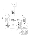
- FIG. 3 is a block diagram illustrating the configuration of a single thread type commit control unit.
- the configuration of the commit control unit 40 included in the control unit 4 of FIG. 1 will be simply illustrated.
- the commit control unit 40 of FIG. 3 instructions of one thread are registered in the CSE 2.
- the commit control unit 40 of FIG. 3 is provided with a released entry selection circuit 41 illustrating a head entry of the CSE 2 for each clock cycle and an execution completion entry selection circuit 46 illustrating the entries of execution completion events of the CSE 2 for each clock cycle.
- the commit control unit 40 of FIG. 3 is provided with a commit scope register selection circuit for selecting a thread having commit events (CSE window selection circuit 43) and a commit scope register for registering commit events of the selected thread (CSE window 44).
- the results of execution when executing operations at the RSA 14, RSE 15, RSF 16, and RSBR 17 are notified from an execution completion report block 48 to the execution completion entry selection circuit 46.
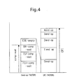
- FIG. 4 is a view illustrating factors of a single thread type CPI.
- the value of the CPI used as one indicator of performance of a processor is found by dividing the number of cycles by the number of executed instructions. If viewing the value of CPI from the perspective of the commit processing, when a number of instructions can be ended in a simultaneous clock cycle, for example, four instructions can be simultaneously committed, the CPI becomes the result of dividing the number of cycles measured for each commit event, that is, 0 end-op (end of zero operations), 1 end-op (end of one operation), 2 end-op (end of two operations), 3 end-op (end of three operations), and 4 end-op (end of four operations), by the number of executed instructions and cumulatively adding the values.
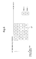
- FIG. 5 is a flow chart illustrating a general super scalar/out-of-order processing
- FIG. 6 is a view conceptually illustrating simultaneous multithreading
- FIG. 7 is a flowchart illustrating processing by simultaneous multithreading.
- a plurality of instruction fetch cycles 100, a plurality of instruction decode (D) cycles 101, and commits (W) of a plurality of instructions 104 are processed in order.
- the plurality of instructions decoded by the plurality of instruction decode (D) cycles 101 are individually executed out of order (plurality of execution cycles 102-1, 102-2, 102-3, and 102-4).
- commit waits 103-1, 103-2, and 103-3 occur.
- simultaneous multithreading having the function of simultaneously executing a plurality of threads (execution cycles) is employed.
- SMT simultaneous multithreading
- two or more threads are simultaneously executed and instructions of the threads are registered in the CSE.
- CSE window By copying into a commit scope register (CSE window) limited to one or more threads like a single thread the entries of commit candidates of threads alternately selected for each clock cycle, commit processing is performed. Performance of each thread is analyzed by the performance analysis circuit.
- the instruction fetch cycle 110, decode cycle 111, execute cycle 112, and commit cycle 113 of the thread A and the instruction fetch cycle 120, decode cycle 121, execute cycle 122, and commit cycle 123 of the thread B are simultaneously executed.
- the instruction fetch cycle 120, decode cycle 121, execute cycle 122, and commit cycle 123 of the thread B are simultaneously executed.
- the commit scope register register In the SMT illustrated in FIG. 6 and FIG. 7 , a plurality of threads are registered in the CSE, but the commit scope register registers only commit candidates of the commit scope register selected by the thread selection circuit for each clock cycle. Accordingly, the commit scope register performs only the commit processing of the selected thread. Further, the events of the selected thread are sent from the commit scope register to the performance analysis circuit.
- FIG. 8 is a block diagram illustrating the configuration of a simultaneous multithreading type commit control unit (thread measurement) according to the present invention
- FIG. 9 is a view illustrating the way of viewing the number of instruction commits of a core
- FIG. 10 is a view illustrating the factors of the CPI of each thread.
- the configuration of a commit control unit 40MS included in a control unit 4M of the later explained FIG. 13 will be simply explained.
- the configuration of the commit control unit 40MS of FIG. 8 is substantially the same as the configuration of the single thread type commit control unit 40 of the above-mentioned FIG. 3 .
- the CSE's 2-1 and 2-2 are separated for the different threads (for example, thread 0 and thread 1). Commit processing is performed at the CSE window 44 for the commit candidates of the thread selected by the thread selection circuit 49.
- the instructions registered at the CSEs 2-1 and 2-2 every clock cycle, four instructions of commit candidates to be next committed in the thread selected by the thread selection circuit 49 are copied in the CSE window 43.
- the commit processing at the completion judgment block 45 it is judged if execution has been completed, if commit processing has been performed for the previous instruction, or if simultaneous commit processing is possible.
- the performance analysis (PA) circuits 3-1 and 3-2 analyze events relating to a thread sent from the CSE window 44 and analyze events relating to not selected threads sent from either of the CSEs 2-1 and 2-2.
- the thread selected by the thread selection circuit 49 is measured for events from the CSE window 44 of 0 end-op (end of zero operations), 1 end-op (end of one operation), 2 end-op (end of two operations), 3 end-op (end of three operations), and 4 end-op (end of four operations), while the not selected threads are measured by the performance analysis circuits 3-1 and 3-2 of the threads judged to be 0 end-op (end of zero operations). Due to this, both the selected thread and the not selected threads can be simultaneously measured for events by the performance analysis circuits 3-1 and 3-2 of the different threads.
- events stored in the CSE window 44 such as EU comp-wait (waiting for completion of operation), BR comp-wait (waiting for completion of branching), and FCH comp-wait (waiting for completion of forwarding of data from cache memory) (all belonging to comp-wait) are analyzed by the performance analysis circuits 3-1 and 3-2 and factors of the 0 end-op are analyzed.
- TOQ comp-wait registers holding events of factors of EU comp-wait (waiting for completion of operation), BR comp-wait (waiting for completion of branching), and FCH comp-wait (waiting for completion of forwarding of data from cache memory) for all threads, it is possible to measure the factors from the TOQ comp-wait register to 0 end-op by the performance analysis circuits 3-1 and 3-2 only when TOQ commit processing is not possible.
- the CPI is comprised of 0 end-op (end of zero operations), 1 end-op (end of one operation)), 2 end-op (end of two operations), 3 end-op (end of three operations), and 4 end-op (end of four operations) as components.
- 0 end-op represents that commit processing of TOQ was not possible
- 1 end-op, 2 end-op, 3 end-op, and 4 end-op represent that commit processing was simultaneously performed for one instruction, two instructions, three instructions, and four instructions from the TOQ.
- the thread selected by the thread selection circuit is measured for events of 0 end-op, 1 end-op, 2 end-op, 3 end-op, and 4 end-op from the CSE window, while the not selected threads are measured by the performance analysis circuit of each thread judging them as 0 end-op whereby both the selected thread and the not selected threads can be simultaneously measured for events by the performance analysis circuits of the different threads.
- FIG. 11 is a block diagram illustrating the configuration of an SMT type commit control unit (core measurement) according to the present invention
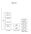
- FIG. 12 is a view illustrating the reasons for the CPI of a core.
- the configuration of a commit control unit 40MC (core measurement) of FIG. 11 is substantially the same as the configuration of the above-mentioned commit control unit 40MS of FIG. 8 (thread measurement).
- the CSEs 2-3 and 2-3 are separated for each thread (for example, thread 0 and thread 1), but are configured as a single one core 2-5.
- the instructions registered in the core 2-5 comprised of the CSEs 2-3 and 2-4 are copied in each clock cycle in the CSE window 44 in groups of four instructions of commit candidates to be next committed in the thread selected by the thread selection circuit 49.
- commit processing at the completion judgment block 45 it is judged if execution has been completed, if the previous instruction has finished being processed by commit processing, or if simultaneous commit processing is possible.
- commit processing is performed simultaneously for a maximum of four instructions for each clock cycle.
- the thread selection circuit 49 when using the thread selection circuit 49 to register just one thread in the CSE window 44 and performing the commit processing for only the selected thread limited to one thread, it becomes possible to measure the event of commit processing corresponding to the thread selected at the CSE window 44. For example, as illustrated in FIG. 9 , in a clock cycle in which all threads have no instruction commits, the processing as a core also has no instruction commits, but in a clock cycle in which one thread has no instruction commits, if the other threads have for example four instruction simultaneous commits, the processing as a core has four instruction simultaneous commits.
- the instruction commit processing is always performed in the CSE window 44, so if obtaining 1 end-op (end of one operation), 2 end-op (end of two operations), 3 end-op (end of three operations), and 4 end-op (end of four operations) for each thread as a means for solution of the first inconvenient situation, it is possible to calculate this by cumulatively adding all threads.
- the factors of CPI that is, Core 0 end-op, Core 1 end-op, Core 2 end-op, Core 3 end-op, and Core 4 end-op and the factors of Core 0 end-op, that is, Core EU comp-wait, Core BR comp-wait, Core FCH comp-wait, and Core CSE-empty, registered the CSE window 44 are analyzed.
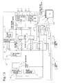
- FIG. 13 is a block diagram illustrating the overall configuration of a simultaneous multithreading processor (SMT type processor) according to the present invention, while FIG. 14 is a view illustrating a simultaneous multithreading type pipeline.
- the configuration of the SMT type processor of FIG. 13 is substantially the same as the configuration of the single thread type processor of FIG. 1 .
- the processing unit 1M is provided with, for the two threads, the CSEs 2-1 and 2-2, fixed decimal point registers 22-1 and 22-2, fixed decimal point registers 25-1 and 25-2, program counters (PC) 26-1 and 26-2, next program counters (NEXT PC) 27-1 and 27-2, and performance analysis (PA) circuits 3-1 and 3-2.
- the other resources are used in common for all threads or are utilized switching threads every clock cycle.
- the primary instruction cache memory 12 sends instructions of the addresses to the instruction decoder 13.
- the instructions of the same thread are decoded in order up to a maximum of four instructions.
- all instructions decoded by the instruction decoder 13 are registered for each thread in the CSEs 2-1 and 2-2 performing the commit processing. Simultaneously with this, they are registered in the RS's controlling the execution of instructions out of order. Instructions not able to be executed by the RS's are loaded out of order in the arithmetic logic units 20 and 23.
- the results of execution of the operations are stored in an update buffer (for example, fixed decimal point update buffer 21 or floating decimal point update buffer 24).
- the CSE's 2-1 and 2-2 receive reports of end of execution of operations, end of transfer of data from the primary data cache memory 19, end of branch judgment from the branch prediction mechanism 11, etc., perform commit processing in order for the same thread simultaneously for up to a maximum of four instructions, store the results from the update buffer in a register (for example, fixed decimal point registers 22-1 and 22-2 or floating decimal point registers 25-1 and 25-2), and update the program counters of the threads.
- the performance analysis circuits 3-1 and 3-2 for analyzing events are circuits for analyzing events from the parts of the processor. Two threads worth are provided for each thread and can analyze events separately for each thread.
- FIG. 14 illustrates an SMT type pipeline.
- SMT the same operation is performed as with a single thread when viewed for each thread on the time axis (t). For example, when cache miss of the thread ($miss) occurs, the commit processing for all of the following instructions ends up stopping in a single thread.
- commit processing of the instructions of the thread 1 is possible, so by alternately using two threads, it becomes possible to raise the operating rate of the commit processing unit.
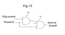
- FIG. 15 is a circuit diagram illustrating one example of an 0 end-op generation circuit of one thread.
- an 0 end-op generation circuit of one thread is comprised of a plurality of logic devices each comprised of an AND device 50 and OR device 51.
- the thread ID of the CSE window (Thread-ID) is 0 (that is, when the thread 0 is assigned priority) and the head instruction cannot be completed (TOQ-commit) or, further, when the Thread-ID is 1 (that is, the thread 1 is assigned priority) and the thread 0 is not selected, an 0 end-op event is generated illustrating that the commit processing of the thread 0 could not be completed. The thus generated 0 end-op event is analyzed by a performance analysis circuit for each thread.
- the components of the 0 end-op event can be classified into an EU comp-wait (waiting for completion of operation), BR comp-wait (waiting for completion of branching), FCH comp-wait (waiting for completion of forwarding of data from cache memory), or other state where conditions of execution completion are not met, state where no thread is selected (CSE priority-wait), or state where nothing is registered in the CSE (CSE empty).
- FIG. 16 is a block diagram illustrating the configuration of an event generation circuit in a commit control unit of the present invention
- FIG. 17 is a view conceptually illustrating the relationship between a CSE window and TOQ comp wait
- FIG. 18 is a timing chart illustrating the timings of set and reset of TOQ comp wait.
- FIG. 16 a specific example of an event generation circuit included in the commit control unit of FIG. 8 is illustrated.
- the event generation circuit of FIG. 16 is comprised of a plurality of logic devices for each thread.
- the thread 0 side event generation circuit is comprised of two AND devices 54-1 and 55-1 and one OR device 56-1.
- one AND device 54-1 has the function of using the thread ID 44N to detect an event representing that an instruction could not be completed due to the thread 0 not being selected
- the other AND device 55-1 has the function of detecting an event representing that an instruction could not be completed due to some reason or another regardless of the thread 0 being selected.
- the thread 1 side event generation circuit is comprised of two AND devices 54-2 and 55-2 and one OR device 56-2.
- one AND device 55-2 has the function of using a thread ID 44N to detect an event representing that an instruction could not be completed since the thread 1 was not selected, while the other AND device 54-2 has the function of detecting an event representing that an instruction could not be completed due to some reason or another despite the thread 1 being selected.
- the state where the conditions for end of execution completion are not met can be analyzed by sending events to the performance analysis circuits 3-1 and 3-2 of the threads.
- execution completion wait events of the head instruction such as EU comp-wait, BR comp-wait, and FCH comp-wait are stored in the TOQ comp-wait registers 52 and 53 of the threads (see FIG. 17 ) and are held until there is no longer any execution completion wait.
- the timing for setting and resetting for TOQ comp-wait is illustrated in the timing chart of FIG. 18 .
- the state in the first and third clock cycles, it is illustrated that when the thread 0 is not selected, the state is one where the conditions for execution completion of the thread 0 are met (set state where flag 1 is set at TOQ comp-wait register of thread 0).
- the state in the second clock cycle, when the thread 1 is selected, the state is one where the conditions for execution completion of the thread 0 are not met (set state where flag 1 is set at TOQ comp-wait register of thread 0).
- the state is one where the conditions for execution completion of the thread 0 are met (reset state where flag 0 is set at TOQ comp-wait register of thread 0).
- the state is the execution completion wait state at the thread 0.
- the thread 0 when the thread 0 is selected, the state becomes one where the execution completion conditions of the thread 0 are met and the completion of commit processing is illustrated.
- FIG. 19 is a circuit diagram illustrating one example of a CSE priority wait generation circuit of one thread.
- the CSE priority-wait generation circuit of one thread is comprised of a logic device comprised of one AND device 57.
- FIG. 20 is a circuit diagram illustrating one example of an 0 end-op generation circuit of a core.
- the 0 end-op generation circuit of the core is comprised of a plurality of logic devices each comprised of two AND devices 58 and 59.
- an 0 end-op generation circuit of a core such as in FIG. 20 in a performance analysis circuit, it is possible to generate an 0 end-op of the thread 0 of the core.
- the thread ID is 0, Core 0 end-op of the thread 0 is generated and measured.
- the thread ID is 1, the Core 0 end-op of the thread 1 is generated and measured.
Landscapes
- Engineering & Computer Science (AREA)
- Theoretical Computer Science (AREA)
- Software Systems (AREA)
- General Engineering & Computer Science (AREA)
- Physics & Mathematics (AREA)
- General Physics & Mathematics (AREA)
- Multimedia (AREA)
- Computer Hardware Design (AREA)
- Quality & Reliability (AREA)
- Advance Control (AREA)
- Debugging And Monitoring (AREA)
- Multi Processors (AREA)
Claims (3)
- Unité de traitement comprenant :une pluralité d'unités d'exécution de fil, chacune agencée pour exécuter un fil ayant une pluralité d'instructions, dans laquelle chaque unité d'exécution de fil est pourvued'un circuit d'analyse de performance (3-1, 3-2) pour mesurer divers types d'événements résultant de l'exécution desdites instructions, etd'une unité d'entrée de pile de validation (2-1, 2-2) pour commander l'achèvement d'instructions exécutées ;caractérisée par :un registre de portée de validation (44) pour stocker des instructions de candidats d'achèvement stockés dans chaque unité d'entrée de pile de validation (2-1, 2-2), où le traitement pour l'achèvement d'instructions est effectué sur la base des instructions dans le registre de portée de validation (44) lorsque chacune de la pluralité d'unités d'exécution de fil achève les instructions exécutées ; etun moyen de sélection de fil (49) pour sélectionner un fil pour lequel des instructions des candidats d'achèvement doivent être copiées de l'unité d'entrée de pile de validation (2-1, 2-2) associée à ce fil sélectionné au registre de portée de validation (44) ;l'unité de traitement est pourvue, pour chaque fil, d'un registre (52, 53) pour, lorsqu'une instruction de tête ne peut pas être achevée par un traitement d'achèvement de l'instruction, contenir un événement d'un facteur en attente d'achèvement, etle moyen de sélection de fil (49) est agencé pour envoyer simultanémentun événement d'un facteur en raison duquel une instruction de tête du fil sélectionné stocké dans le registre de portée de validation n'a pas pu être achevée au circuit d'analyse de performance (3-1, 3-2) du fil sélectionné afin d'analyser ainsi le facteur en raison duquel l'instruction de tête du fil n'a pas pu être achevée, etun événement d'un facteur stocké dans le registre (52, 53) d'un fil non sélectionné au circuit d'analyse de performance (3-1, 3-2).
- Unité de traitement selon la revendication 1, dans laquelle le circuit générant un événement d'un facteur en raison duquel l'instruction de tête du fil stocké dans le registre de portée de validation n'a pas pu être achevée et un événement d'un facteur stocké dans un registre contenant un facteur d'uniquement quand une instruction de tête d'un autre fil n'a pas pu être achevée se compose d'une combinaison d'une pluralité de dispositifs logiques.
- Unité de traitement selon la revendication 1, qui divise les événements de validation pour chaque fil par le nombre d'instructions exécutées pour chaque fil et ajoute cumulativement les valeurs pour tous les événements de validation des fils respectifs afin d'analyser les facteurs de la valeur moyenne du nombre de cycles d'horloge requis pour l'achèvement d'une instruction d'un programme.
Applications Claiming Priority (1)
| Application Number | Priority Date | Filing Date | Title |
|---|---|---|---|
| PCT/JP2007/062445 WO2008155845A1 (fr) | 2007-06-20 | 2007-06-20 | Processeur |
Publications (3)
| Publication Number | Publication Date |
|---|---|
| EP2159685A1 EP2159685A1 (fr) | 2010-03-03 |
| EP2159685A4 EP2159685A4 (fr) | 2010-12-08 |
| EP2159685B1 true EP2159685B1 (fr) | 2013-08-21 |
Family
ID=40156011
Family Applications (1)
| Application Number | Title | Priority Date | Filing Date |
|---|---|---|---|
| EP07767283.0A Not-in-force EP2159685B1 (fr) | 2007-06-20 | 2007-06-20 | Processeur |
Country Status (4)
| Country | Link |
|---|---|
| US (1) | US8001362B2 (fr) |
| EP (1) | EP2159685B1 (fr) |
| JP (1) | JP5136553B2 (fr) |
| WO (1) | WO2008155845A1 (fr) |
Families Citing this family (2)
| Publication number | Priority date | Publication date | Assignee | Title |
|---|---|---|---|---|
| GB2489708B (en) * | 2011-04-05 | 2020-04-15 | Advanced Risc Mach Ltd | Thread selection for multithreaded processing |
| US10977075B2 (en) * | 2019-04-10 | 2021-04-13 | Mentor Graphics Corporation | Performance profiling for a multithreaded processor |
Family Cites Families (14)
| Publication number | Priority date | Publication date | Assignee | Title |
|---|---|---|---|---|
| US5835705A (en) * | 1997-03-11 | 1998-11-10 | International Business Machines Corporation | Method and system for performance per-thread monitoring in a multithreaded processor |
| US6076157A (en) * | 1997-10-23 | 2000-06-13 | International Business Machines Corporation | Method and apparatus to force a thread switch in a multithreaded processor |
| US6052709A (en) * | 1997-12-23 | 2000-04-18 | Bright Light Technologies, Inc. | Apparatus and method for controlling delivery of unsolicited electronic mail |
| US6535905B1 (en) * | 1999-04-29 | 2003-03-18 | Intel Corporation | Method and apparatus for thread switching within a multithreaded processor |
| JP3512678B2 (ja) | 1999-05-27 | 2004-03-31 | 富士通株式会社 | キャッシュメモリ制御装置および計算機システム |
| US6791367B2 (en) * | 2002-03-19 | 2004-09-14 | Broadcom Corporation | Hardware and software programmable fuses for memory repair |
| US7472258B2 (en) * | 2003-04-21 | 2008-12-30 | International Business Machines Corporation | Dynamically shared group completion table between multiple threads |
| US7657893B2 (en) * | 2003-04-23 | 2010-02-02 | International Business Machines Corporation | Accounting method and logic for determining per-thread processor resource utilization in a simultaneous multi-threaded (SMT) processor |
| US7360062B2 (en) | 2003-04-25 | 2008-04-15 | International Business Machines Corporation | Method and apparatus for selecting an instruction thread for processing in a multi-thread processor |
| US20050138333A1 (en) * | 2003-12-19 | 2005-06-23 | Samra Nicholas G. | Thread switching mechanism |
| US20050183065A1 (en) * | 2004-02-13 | 2005-08-18 | Wolczko Mario I. | Performance counters in a multi-threaded processor |
| JP2005284749A (ja) * | 2004-03-30 | 2005-10-13 | Kyushu Univ | 並列処理コンピュータ |
| JP4327008B2 (ja) * | 2004-04-21 | 2009-09-09 | 富士通株式会社 | 演算処理装置及び演算処理装置の制御方法 |
| JP4486434B2 (ja) * | 2004-07-29 | 2010-06-23 | 富士通株式会社 | 命令リトライ検証機能付き情報処理装置および命令リトライ検証方法 |
-
2007
- 2007-06-20 JP JP2009520199A patent/JP5136553B2/ja not_active Expired - Fee Related
- 2007-06-20 WO PCT/JP2007/062445 patent/WO2008155845A1/fr not_active Ceased
- 2007-06-20 EP EP07767283.0A patent/EP2159685B1/fr not_active Not-in-force
-
2009
- 2009-12-08 US US12/633,108 patent/US8001362B2/en active Active
Also Published As
| Publication number | Publication date |
|---|---|
| EP2159685A1 (fr) | 2010-03-03 |
| JPWO2008155845A1 (ja) | 2010-08-26 |
| US20100088491A1 (en) | 2010-04-08 |
| US8001362B2 (en) | 2011-08-16 |
| EP2159685A4 (fr) | 2010-12-08 |
| WO2008155845A1 (fr) | 2008-12-24 |
| JP5136553B2 (ja) | 2013-02-06 |
Similar Documents
| Publication | Publication Date | Title |
|---|---|---|
| KR101994636B1 (ko) | 데이터 처리장치의 추적 | |
| US5691920A (en) | Method and system for performance monitoring of dispatch unit efficiency in a processing system | |
| US6708296B1 (en) | Method and system for selecting and distinguishing an event sequence using an effective address in a processing system | |
| US5797019A (en) | Method and system for performance monitoring time lengths of disabled interrupts in a processing system | |
| US5752062A (en) | Method and system for performance monitoring through monitoring an order of processor events during execution in a processing system | |
| US5751945A (en) | Method and system for performance monitoring stalls to identify pipeline bottlenecks and stalls in a processing system | |
| US7086035B1 (en) | Method and system for counting non-speculative events in a speculative processor | |
| EP3320427B1 (fr) | Dispositif et architecture de traitement permettant une efficacité de mémoire d'instructions | |
| JP4467093B2 (ja) | プロセッサパイプラインにおいて命令をランダムにサンプリングする装置 | |
| US9720695B2 (en) | System for providing trace data in a data processor having a pipelined architecture | |
| CN100458727C (zh) | 同时多线程处理器内核及其核算处理器时间利用的方法 | |
| US5949971A (en) | Method and system for performance monitoring through identification of frequency and length of time of execution of serialization instructions in a processing system | |
| US9952871B2 (en) | Controlling execution of instructions for a processing pipeline having first out-of order execution circuitry and second execution circuitry | |
| US6338133B1 (en) | Measured, allocation of speculative branch instructions to processor execution units | |
| US6530042B1 (en) | Method and apparatus for monitoring the performance of internal queues in a microprocessor | |
| US20100031006A1 (en) | Thread completion rate controlled scheduling | |
| US5729726A (en) | Method and system for performance monitoring efficiency of branch unit operation in a processing system | |
| US5748855A (en) | Method and system for performance monitoring of misaligned memory accesses in a processing system | |
| US20120046912A1 (en) | Processor core having a saturating event counter for making performance measurements | |
| US6550002B1 (en) | Method and system for detecting a flush of an instruction without a flush indicator | |
| US20100095305A1 (en) | Simultaneous multithread instruction completion controller | |
| US8001362B2 (en) | Processing unit | |
| US8561079B2 (en) | Inter-thread load arbitration control detecting information registered in commit stack entry units and controlling instruction input control unit | |
| US20040128476A1 (en) | Scheme to simplify instruction buffer logic supporting multiple strands | |
| WO2017199106A1 (fr) | Fils d'exécution multiples spéculatifs à fil unique |
Legal Events
| Date | Code | Title | Description |
|---|---|---|---|
| PUAI | Public reference made under article 153(3) epc to a published international application that has entered the european phase |
Free format text: ORIGINAL CODE: 0009012 |
|
| 17P | Request for examination filed |
Effective date: 20100113 |
|
| AK | Designated contracting states |
Kind code of ref document: A1 Designated state(s): AT BE BG CH CY CZ DE DK EE ES FI FR GB GR HU IE IS IT LI LT LU LV MC MT NL PL PT RO SE SI SK TR |
|
| AX | Request for extension of the european patent |
Extension state: AL BA HR MK RS |
|
| DAX | Request for extension of the european patent (deleted) | ||
| A4 | Supplementary search report drawn up and despatched |
Effective date: 20101110 |
|
| RIC1 | Information provided on ipc code assigned before grant |
Ipc: G06F 9/38 20060101ALI20101104BHEP Ipc: G06F 11/34 20060101AFI20101104BHEP |
|
| 17Q | First examination report despatched |
Effective date: 20110809 |
|
| GRAP | Despatch of communication of intention to grant a patent |
Free format text: ORIGINAL CODE: EPIDOSNIGR1 |
|
| GRAS | Grant fee paid |
Free format text: ORIGINAL CODE: EPIDOSNIGR3 |
|
| GRAA | (expected) grant |
Free format text: ORIGINAL CODE: 0009210 |
|
| AK | Designated contracting states |
Kind code of ref document: B1 Designated state(s): AT BE BG CH CY CZ DE DK EE ES FI FR GB GR HU IE IS IT LI LT LU LV MC MT NL PL PT RO SE SI SK TR |
|
| REG | Reference to a national code |
Ref country code: GB Ref legal event code: FG4D |
|
| REG | Reference to a national code |
Ref country code: CH Ref legal event code: EP |
|
| REG | Reference to a national code |
Ref country code: AT Ref legal event code: REF Ref document number: 628453 Country of ref document: AT Kind code of ref document: T Effective date: 20130915 |
|
| REG | Reference to a national code |
Ref country code: IE Ref legal event code: FG4D |
|
| REG | Reference to a national code |
Ref country code: DE Ref legal event code: R096 Ref document number: 602007032398 Country of ref document: DE Effective date: 20131017 |
|
| REG | Reference to a national code |
Ref country code: NL Ref legal event code: VDEP Effective date: 20130821 Ref country code: AT Ref legal event code: MK05 Ref document number: 628453 Country of ref document: AT Kind code of ref document: T Effective date: 20130821 |
|
| REG | Reference to a national code |
Ref country code: LT Ref legal event code: MG4D |
|
| PG25 | Lapsed in a contracting state [announced via postgrant information from national office to epo] |
Ref country code: PT Free format text: LAPSE BECAUSE OF FAILURE TO SUBMIT A TRANSLATION OF THE DESCRIPTION OR TO PAY THE FEE WITHIN THE PRESCRIBED TIME-LIMIT Effective date: 20131223 Ref country code: LT Free format text: LAPSE BECAUSE OF FAILURE TO SUBMIT A TRANSLATION OF THE DESCRIPTION OR TO PAY THE FEE WITHIN THE PRESCRIBED TIME-LIMIT Effective date: 20130821 Ref country code: IS Free format text: LAPSE BECAUSE OF FAILURE TO SUBMIT A TRANSLATION OF THE DESCRIPTION OR TO PAY THE FEE WITHIN THE PRESCRIBED TIME-LIMIT Effective date: 20131221 Ref country code: AT Free format text: LAPSE BECAUSE OF FAILURE TO SUBMIT A TRANSLATION OF THE DESCRIPTION OR TO PAY THE FEE WITHIN THE PRESCRIBED TIME-LIMIT Effective date: 20130821 Ref country code: SE Free format text: LAPSE BECAUSE OF FAILURE TO SUBMIT A TRANSLATION OF THE DESCRIPTION OR TO PAY THE FEE WITHIN THE PRESCRIBED TIME-LIMIT Effective date: 20130821 Ref country code: CY Free format text: LAPSE BECAUSE OF FAILURE TO SUBMIT A TRANSLATION OF THE DESCRIPTION OR TO PAY THE FEE WITHIN THE PRESCRIBED TIME-LIMIT Effective date: 20130821 |
|
| PG25 | Lapsed in a contracting state [announced via postgrant information from national office to epo] |
Ref country code: SI Free format text: LAPSE BECAUSE OF FAILURE TO SUBMIT A TRANSLATION OF THE DESCRIPTION OR TO PAY THE FEE WITHIN THE PRESCRIBED TIME-LIMIT Effective date: 20130821 Ref country code: BE Free format text: LAPSE BECAUSE OF FAILURE TO SUBMIT A TRANSLATION OF THE DESCRIPTION OR TO PAY THE FEE WITHIN THE PRESCRIBED TIME-LIMIT Effective date: 20130821 Ref country code: FI Free format text: LAPSE BECAUSE OF FAILURE TO SUBMIT A TRANSLATION OF THE DESCRIPTION OR TO PAY THE FEE WITHIN THE PRESCRIBED TIME-LIMIT Effective date: 20130821 Ref country code: LV Free format text: LAPSE BECAUSE OF FAILURE TO SUBMIT A TRANSLATION OF THE DESCRIPTION OR TO PAY THE FEE WITHIN THE PRESCRIBED TIME-LIMIT Effective date: 20130821 Ref country code: GR Free format text: LAPSE BECAUSE OF FAILURE TO SUBMIT A TRANSLATION OF THE DESCRIPTION OR TO PAY THE FEE WITHIN THE PRESCRIBED TIME-LIMIT Effective date: 20131122 Ref country code: PL Free format text: LAPSE BECAUSE OF FAILURE TO SUBMIT A TRANSLATION OF THE DESCRIPTION OR TO PAY THE FEE WITHIN THE PRESCRIBED TIME-LIMIT Effective date: 20130821 |
|
| PG25 | Lapsed in a contracting state [announced via postgrant information from national office to epo] |
Ref country code: DK Free format text: LAPSE BECAUSE OF FAILURE TO SUBMIT A TRANSLATION OF THE DESCRIPTION OR TO PAY THE FEE WITHIN THE PRESCRIBED TIME-LIMIT Effective date: 20130821 Ref country code: SK Free format text: LAPSE BECAUSE OF FAILURE TO SUBMIT A TRANSLATION OF THE DESCRIPTION OR TO PAY THE FEE WITHIN THE PRESCRIBED TIME-LIMIT Effective date: 20130821 Ref country code: RO Free format text: LAPSE BECAUSE OF FAILURE TO SUBMIT A TRANSLATION OF THE DESCRIPTION OR TO PAY THE FEE WITHIN THE PRESCRIBED TIME-LIMIT Effective date: 20130821 Ref country code: CZ Free format text: LAPSE BECAUSE OF FAILURE TO SUBMIT A TRANSLATION OF THE DESCRIPTION OR TO PAY THE FEE WITHIN THE PRESCRIBED TIME-LIMIT Effective date: 20130821 Ref country code: NL Free format text: LAPSE BECAUSE OF FAILURE TO SUBMIT A TRANSLATION OF THE DESCRIPTION OR TO PAY THE FEE WITHIN THE PRESCRIBED TIME-LIMIT Effective date: 20130821 Ref country code: EE Free format text: LAPSE BECAUSE OF FAILURE TO SUBMIT A TRANSLATION OF THE DESCRIPTION OR TO PAY THE FEE WITHIN THE PRESCRIBED TIME-LIMIT Effective date: 20130821 |
|
| PG25 | Lapsed in a contracting state [announced via postgrant information from national office to epo] |
Ref country code: IT Free format text: LAPSE BECAUSE OF FAILURE TO SUBMIT A TRANSLATION OF THE DESCRIPTION OR TO PAY THE FEE WITHIN THE PRESCRIBED TIME-LIMIT Effective date: 20130821 Ref country code: ES Free format text: LAPSE BECAUSE OF FAILURE TO SUBMIT A TRANSLATION OF THE DESCRIPTION OR TO PAY THE FEE WITHIN THE PRESCRIBED TIME-LIMIT Effective date: 20130821 |
|
| PLBE | No opposition filed within time limit |
Free format text: ORIGINAL CODE: 0009261 |
|
| STAA | Information on the status of an ep patent application or granted ep patent |
Free format text: STATUS: NO OPPOSITION FILED WITHIN TIME LIMIT |
|
| 26N | No opposition filed |
Effective date: 20140522 |
|
| REG | Reference to a national code |
Ref country code: DE Ref legal event code: R097 Ref document number: 602007032398 Country of ref document: DE Effective date: 20140522 |
|
| PG25 | Lapsed in a contracting state [announced via postgrant information from national office to epo] |
Ref country code: LU Free format text: LAPSE BECAUSE OF FAILURE TO SUBMIT A TRANSLATION OF THE DESCRIPTION OR TO PAY THE FEE WITHIN THE PRESCRIBED TIME-LIMIT Effective date: 20140620 Ref country code: MC Free format text: LAPSE BECAUSE OF FAILURE TO SUBMIT A TRANSLATION OF THE DESCRIPTION OR TO PAY THE FEE WITHIN THE PRESCRIBED TIME-LIMIT Effective date: 20130821 |
|
| REG | Reference to a national code |
Ref country code: CH Ref legal event code: PL |
|
| REG | Reference to a national code |
Ref country code: IE Ref legal event code: MM4A |
|
| PG25 | Lapsed in a contracting state [announced via postgrant information from national office to epo] |
Ref country code: IE Free format text: LAPSE BECAUSE OF NON-PAYMENT OF DUE FEES Effective date: 20140620 Ref country code: LI Free format text: LAPSE BECAUSE OF NON-PAYMENT OF DUE FEES Effective date: 20140630 Ref country code: CH Free format text: LAPSE BECAUSE OF NON-PAYMENT OF DUE FEES Effective date: 20140630 |
|
| PG25 | Lapsed in a contracting state [announced via postgrant information from national office to epo] |
Ref country code: MT Free format text: LAPSE BECAUSE OF FAILURE TO SUBMIT A TRANSLATION OF THE DESCRIPTION OR TO PAY THE FEE WITHIN THE PRESCRIBED TIME-LIMIT Effective date: 20130821 |
|
| REG | Reference to a national code |
Ref country code: FR Ref legal event code: PLFP Year of fee payment: 10 |
|
| PG25 | Lapsed in a contracting state [announced via postgrant information from national office to epo] |
Ref country code: BG Free format text: LAPSE BECAUSE OF FAILURE TO SUBMIT A TRANSLATION OF THE DESCRIPTION OR TO PAY THE FEE WITHIN THE PRESCRIBED TIME-LIMIT Effective date: 20130821 |
|
| PG25 | Lapsed in a contracting state [announced via postgrant information from national office to epo] |
Ref country code: TR Free format text: LAPSE BECAUSE OF FAILURE TO SUBMIT A TRANSLATION OF THE DESCRIPTION OR TO PAY THE FEE WITHIN THE PRESCRIBED TIME-LIMIT Effective date: 20130821 Ref country code: HU Free format text: LAPSE BECAUSE OF FAILURE TO SUBMIT A TRANSLATION OF THE DESCRIPTION OR TO PAY THE FEE WITHIN THE PRESCRIBED TIME-LIMIT; INVALID AB INITIO Effective date: 20070620 |
|
| REG | Reference to a national code |
Ref country code: FR Ref legal event code: PLFP Year of fee payment: 11 |
|
| REG | Reference to a national code |
Ref country code: FR Ref legal event code: PLFP Year of fee payment: 12 |
|
| PGFP | Annual fee paid to national office [announced via postgrant information from national office to epo] |
Ref country code: FR Payment date: 20230510 Year of fee payment: 17 Ref country code: DE Payment date: 20230502 Year of fee payment: 17 |
|
| PGFP | Annual fee paid to national office [announced via postgrant information from national office to epo] |
Ref country code: GB Payment date: 20230427 Year of fee payment: 17 |
|
| REG | Reference to a national code |
Ref country code: DE Ref legal event code: R119 Ref document number: 602007032398 Country of ref document: DE |
|
| GBPC | Gb: european patent ceased through non-payment of renewal fee |
Effective date: 20240620 |
|
| PG25 | Lapsed in a contracting state [announced via postgrant information from national office to epo] |
Ref country code: DE Free format text: LAPSE BECAUSE OF NON-PAYMENT OF DUE FEES Effective date: 20250101 |
|
| PG25 | Lapsed in a contracting state [announced via postgrant information from national office to epo] |
Ref country code: FR Free format text: LAPSE BECAUSE OF NON-PAYMENT OF DUE FEES Effective date: 20240630 |
|
| PG25 | Lapsed in a contracting state [announced via postgrant information from national office to epo] |
Ref country code: GB Free format text: LAPSE BECAUSE OF NON-PAYMENT OF DUE FEES Effective date: 20240620 |