EP2164199A2 - Transmetteur de lumière de polarisation multiplexée et son procédé de commande - Google Patents
Transmetteur de lumière de polarisation multiplexée et son procédé de commande Download PDFInfo
- Publication number
- EP2164199A2 EP2164199A2 EP09169702A EP09169702A EP2164199A2 EP 2164199 A2 EP2164199 A2 EP 2164199A2 EP 09169702 A EP09169702 A EP 09169702A EP 09169702 A EP09169702 A EP 09169702A EP 2164199 A2 EP2164199 A2 EP 2164199A2
- Authority
- EP
- European Patent Office
- Prior art keywords
- polarization
- section
- light
- optical
- interfering
- Prior art date
- Legal status (The legal status is an assumption and is not a legal conclusion. Google has not performed a legal analysis and makes no representation as to the accuracy of the status listed.)
- Withdrawn
Links
Images










Classifications
-
- H—ELECTRICITY
- H04—ELECTRIC COMMUNICATION TECHNIQUE
- H04J—MULTIPLEX COMMUNICATION
- H04J14/00—Optical multiplex systems
- H04J14/06—Polarisation multiplex systems
-
- H—ELECTRICITY
- H04—ELECTRIC COMMUNICATION TECHNIQUE
- H04B—TRANSMISSION
- H04B10/00—Transmission systems employing electromagnetic waves other than radio-waves, e.g. infrared, visible or ultraviolet light, or employing corpuscular radiation, e.g. quantum communication
- H04B10/50—Transmitters
- H04B10/501—Structural aspects
- H04B10/503—Laser transmitters
- H04B10/505—Laser transmitters using external modulation
- H04B10/5053—Laser transmitters using external modulation using a parallel, i.e. shunt, combination of modulators
-
- H—ELECTRICITY
- H04—ELECTRIC COMMUNICATION TECHNIQUE
- H04B—TRANSMISSION
- H04B10/00—Transmission systems employing electromagnetic waves other than radio-waves, e.g. infrared, visible or ultraviolet light, or employing corpuscular radiation, e.g. quantum communication
- H04B10/50—Transmitters
- H04B10/501—Structural aspects
- H04B10/503—Laser transmitters
- H04B10/505—Laser transmitters using external modulation
- H04B10/5057—Laser transmitters using external modulation using a feedback signal generated by analysing the optical output
-
- H—ELECTRICITY
- H04—ELECTRIC COMMUNICATION TECHNIQUE
- H04B—TRANSMISSION
- H04B10/00—Transmission systems employing electromagnetic waves other than radio-waves, e.g. infrared, visible or ultraviolet light, or employing corpuscular radiation, e.g. quantum communication
- H04B10/50—Transmitters
- H04B10/516—Details of coding or modulation
- H04B10/532—Polarisation modulation
-
- H—ELECTRICITY
- H04—ELECTRIC COMMUNICATION TECHNIQUE
- H04B—TRANSMISSION
- H04B10/00—Transmission systems employing electromagnetic waves other than radio-waves, e.g. infrared, visible or ultraviolet light, or employing corpuscular radiation, e.g. quantum communication
- H04B10/50—Transmitters
- H04B10/58—Compensation for non-linear transmitter output
Definitions
- the embodiments discusses herein are directed to a polarization multiplexed light transmitter which applies a polarization multiplexing technology to transmit optical signals in optical communications and a control method thereof.
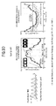
- bit-interleaved polarization multiplexing which shifts pulses of the orthogonal polarization components to each other by a half bit, achieves excellent transmission characteristics (refer to the right side of FIG. 30 ).
- bit-aligned polarization multiplexing which makes the pulse timing between the orthogonal polarization components in the polarization multiplexed light to be in-phase, achieves the excellent transmission characteristics (refer to the center of FIG. 30 ). Accordingly, in order to obtain desired transmission characteristics, it is necessary to set the above pulse timing according to a state of the optical transmission system.
- the invention has been accomplished in view of the above problems and has the objective to provide a polarization multiplexed light transmitter capable of flexibly varying a delay time between orthogonal polarization components in a polarization multiplexed light with a simple configuration, and also, capable of suppressing transmission characteristics degradation of the polarization multiplexed light due to a change in system state; and a control method thereof.
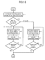
- a polarization multiplexed light transmitter which transmits a polarization multiplexed light containing a first optical signal and a second optical signal of which polarization states are mutually orthogonal, includes: a delay regulating unit configured to regulate relative delay times of the first and second optical signals; and a delay control unit configured to make orthogonal polarization components contained in a monitor light which is obtained by taking out a part of the polarization multiplexed light to interfere with each other, to thereby generate a polarization interfering light, and configured to judge a delay time between the first and second optical signals based on a change in state of an electric signal which is obtained by photo-electrically converting the polarization interfering light, and configured to control regulation amounts in the delay regulating unit so that the judged delay time reaches a predetermined value.
- the conventional polarization multiplexing optical transmission system has a problem in that pulse timing between orthogonal polarization components is not adjustable according to a change in system state.
- the applicant of this invention has proposed, in the prior Japanese Patent Application No. 2008-119011 , a technology for: receiving, in a reception unit, a polarization multiplexed light transmitted from a transmission unit to an optical transmission path; monitoring information relating to transmission characteristics of the received polarization multiplexed light to transfer a monitoring result to the transmission unit; and controlling, in the transmission unit, an inter-polarized channel delay time based on the transmission characteristics information from the reception unit.
- This prior invention is effective for solving the above problem, but a configuration of a control system is complicated. Further, a feedback loop made up between the transmission unit and the reception unit is long, and therefore, a problem in that a control time is long still remains.
- this invention proposes a polarization multiplexed light transmitter capable of flexibly varying at a high speed, with a simple configuration, a delay time between the orthogonal polarization components in the polarization multiplexed light, and also, capable of suppressing transmission characteristics degradation of the polarization multiplexed light due to the change in system state; and a control method thereof.
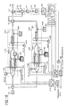
- FIG. 1 is a block diagram illustrating a configuration of a polarization multiplexed light transmitter in a first embodiment.
- the polarization multiplexed light transmitter in the first embodiment comprises: a light source section 11; a polarization separating section 12; a pair of optical modulating sections 13A, 13B: a pair of modulation driving sections 14A, 14B; a polarization combining section 15; a delay regulating unit 20; and a delay control unit 30.
- the delay regulating unit 20 includes a pair of delay amount varying sections 21A and 21B
- the delay control unit 30 includes an optical branching section 31, a polarization interfering section 32, a photoelectric conversion section 33, a signal processing section 34, a power measuring section 35 and a delay control section 36.
- the light source section 11 generates a continuous light or an optical pulse train having a required wavelength, to output it to the polarization separating section 12.
- the polarization separating section 12 separates the output light from the light source section 11 to two lights of which polarization states are mutually orthogonal, and outputs one of the two lights to the optical modulating section 13A while outputting the other light to the optical modulating section 13B.
- the optical modulating sections 13A and 13B modulate the input lights in accordance with modulation signals output from the modulation driving sections 14A and 14B, and thus, generate first and second optical signals (sometimes to be referred to as polarized channels, hereunder) corresponding to a desired optical modulation format, to thereby output the first and second optical signals to the polarization combining section 15.
- first and second optical signals sometimes to be referred to as polarized channels, hereunder
- an intensity modulation format such as NRZ (Non Return to Zero), RZ (Return to Zero), CS-RZ (Carrier-Suppressed Return to Zero), Duobinary or the like
- a phase modulation format such as QPSK (Quadrature Phase Shit Keying), DQPSK (Differential Quadrature Phase Shift Keying), DBPSK (Differential Binary Phase Shift Keying) or the like
- QPSK Quadratture Phase Shit Keying
- DQPSK Differential Quadrature Phase Shift Keying
- DBPSK Differential Binary Phase Shift Keying
- the modulation driving sections 14A and 14B generate the modulation signals corresponding to the modulation format of the optical modulating sections 13A and 13B, in accordance with transmission data fed from the outside or the like, to supply them to the optical modulating sections 13A and 13B via the delay amount varying sections 21 A and 21B.
- the polarization combining section 15 combines the orthogonal polarized optical signals output from the optical modulating sections 13A and 13B into one light.
- the combined polarization multiplexed light passes through the optical branching section 31 in the delay control unit 30 to be transmitted from an output port OUT of the present polarization multiplexed light transmitted to the outside.
- the configuration example is described in which the two polarization components are branched and combined using the polarization branching section 12 and the polarization combining section 15.
- this invention is not limited thereto, and it is also possible to apply a configuration in which an optical branching section 16.
- polarization regulating sections 17A and 17B, and an optical multiplexing section 18 are combined with each other, as illustrated in an upper stage of FIG. 2 .
- the output light form the light source section 11 is branched into two lights by the optical branching section 16, and thereafter, the two branched lights are respectively modulated by the optical modulating sections 13A and 13B, and the respective modulated lights are input to the corresponding polarization regulating sections 17A and 17B.
- polarization states of the two modulated lights are regulated to be mutually orthogonal.
- a ⁇ /4 plate may be disposed to one of the polarization regulating sections 17A and 17B while a - ⁇ /4 plate being disposed to the other thereof, to make the polarization states of the two modulated lights to be mutually orthogonal.
- a ⁇ /2 plate may be disposed to one of the polarization sections 17A and 17B, to realize the orthogonal polarization.
- variable polarization controlling devices may be disposed to both the polarization regulating sections 17A and 17B and the respective output lights are fed back, to thereby regulate the polarization states of the two modulated lights to be mutually orthogonal Then, the output lights from the polarization regulating sections 17A and 17B are fed to the optical multiplexing section 18 so that the polarization multiplexed light is generated. Further, it is also possible to apply a configuration in which two light sources 11A and 11B are used as the light source section 11 and output lights from the light sources 11A anti 11B are supplied to the optical modulating sections 13A and 13B, as illustrated in a lower stage of FIG 2 . In this case, it is possible to realize the light source section 11 by using two low power light sources.
- the optical branching section 31 branches a part of the polarization multiplexed light sent from the polarization combining section 15 to the output port OUT as a monitor light, to output the monitor light to the polarization interfering section 32.
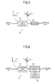
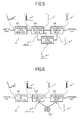
- the polarization interfering section 32 makes the orthogonal polarization components (polarized channels) contained in the monitor light from the optical branching section 31 to interfere with each other, to generate a polarization interfering light, and outputs the polarization interfering light to the photoelectric conversion section 33. It is possible to realize such a polarization interfering section 32 by various types of configurations as illustrated in FIG. 3 to FIG. 7 for example.
- a first configuration example of the polarization interfering section 32 illustrated in FIG. 3 includes a polarization angle regulator 321 and a polarizer 322.
- the polarization angle regulator 321 is fed with the monitor light from the optical blanching section 31, and regulates a polarization angle of the monitor light so that polarization directions of orthogonal polarized channels "x" and "y” in the monitor light are deviated from a direction of main axis "a" of the polarizer 322.
- a z-direction illustrated by a broken line arrow in the figure indicates an optical axis direction of the monitor light.
- the polarizer 322 is fed with the monitor light of which polarization angle is regulated by the polarization angle regulator 321, thereby generating a light obtained by making the polarized channels "x" and “y” in the monitor light to interfere with each other, to output the polarization interfering light to the photoelectric conversion section 33.
- a deviation angle of the polarization direction of the one polarized channel "y" relative to the direction of the main axis "a" of the polarizer 322 is ⁇
- this deviation angle ⁇ is desirable to be 45°+360°xN (N is integer).
- N is integer
- a second configuration example of the polarization interfering section 32 illustrated in FIG. 4 applies a polarization separating device 323 in place of the polarizer 322 in the first configuration example of FIG. 3 .
- the polarization angle regulator 321 the polarization angle of the monitor light is regulated, so that the polarization directions of the orthogonal polarized channels "x" and "y" in the monitor light output from the optical branching section 31 are deviated from a direction of a main axis "a" of the polarization separating device 323 (desirably, the deviation angle ⁇ is to be 45°+360°xN).
- the polarization separating device 323 is fed with the output light from the polarization angle regulator 321 to generate a light obtained by making the polarized channels "x" and “y” in the monitor light to interfere with each other, to thereby output the polarization interfering light from first and second output ports thereof.
- the polarization interfering light output from the first output port of the polarization separating device 323 is sent to the photoelectric conversion section 33, and an optical terminator 324 is connected to the second output port of the polarization separating device 323.
- a branching port of the optical branching section 31 may be connected via a polarization-preservation fiber to an input port of the polarizer 322 or the polarization separating device 323, to thereby add required angle deviation when the polarization-preservation fiber is splice connected to the respective ports.
- a polarization angle regulator 325 is connected to the second output port of the polarization separating device 323, and further, a polarization combining device 326 is disposed for combining an output light from the polarization angle regulator 325 with the output light from the first output port of the polarization separating device 323.
- the polarization angle of the monitor light is regulated by the polarization angle regulator 321, so that the polarization direction of one of the orthogonal polarized channels "x" and “y” in the monitor light output from the optical branching section 31 (herein, the polarization direction of the polarized channel "y") is coincident with the main axis "a" of the polarization separating device 323.
- the output light from the polarization angle regulator 325 is fed to the polarization separating device 323, so that the polarized channel "y” is output from the first output port of the polarization separating device 323, whereas the polarized channel "x” is output from the second output port of the polarization separating device 323.
- the polarization direction of the polarized channel "x" output from the second output port of the polarization separating device 323 is rotated by 90° in the polarization angle regulator 325, to be in the same polarization direction as that of the polarized channel "y". Then, the polarized channel "y" output from the first output port of the polarization separating device 323 and the polarized channel "x" of which polarization direction is rotated by 90° by the polarization angle regulator 325, are input to the polarization combining device 326, so that the light obtained by making the polarized channels "x" and "y” to interfere with each other is generated, and the polarization interfering light is sent to the photoelectric conversion section 33.
- a faraday rotating mirror (FRM) 327 is disposed in place of the polarization angle regulator 325 used in the third configuration example of FIG. 5 .
- the FRM 327 has optical characteristics of rotating a polarization angle by 90° when reflecting an incident light.
- the polarized channel "x" output from the second output port of the polarization separating device 323 is reflected from the FRM 327, so that the polarization direction of the polarized channel "x" is made to be same as that of the polarized channel "y".
- the light obtained by making the polarized channels "x" and “y” to interfere with each other is generated in the polarization combining device 326, and the polarization interfering light is sent to the photoelectric conversion section 33.
- a fifth configuration example of the polarization interfering section 32 illustrated in FIG. 7 includes an optical amplifier 328 and a nonlinear element 329.
- the optical amplifier 328 receives the monitor light from the optical branching section 31, and amplifies the power of the monitor light up to a level at which a nonlinear effect can be generated in the latter staged nonlinear element 329, to output the amplified monitor light.
- the nonlinear element 329 receives the monitor light amplified by the optical amplifier 328 and a control light fed from the outside or the like, and similarly to an operating principle of a known optical Kerr switch, rotates the polarization directions of the polarized channels in the monitor light, by cross phase modulation (XPM) which is one of nonlinear effects.
- XPM cross phase modulation
- the polarization direction of the polarized channel "x" in the monitor light is rotated by a predetermined angle ⁇ , by XPM generated in the nonlinear element 329, so that a component, which is parallel to the polarized channel "y", in the rotated polarized channel "x”, and the polarized channel "y” interfere with each other, and consequently, the polarization interfering light is sent to the photoelectric conversion section 33 from the nonlinear element 329.
- the first to fifth configuration examples for the polarization interfering section 32 have been recited.
- the polarization interfering section to be used in the invention is not limited to the above configuration examples, and it is possible to apply arbitrary configurations capable of making the orthogonal polarized channels "x" and "y" in the monitor light to interfere with each other.
- the inter-polarized channel delay time is variably controlled in an electric signal (modulation signal) stage thereof by the delay amount varying sections 21A and 21B
- the inter-polarized channel delay time is variably controlled in an optical signal stage thereof.
- optical delay amount varying sections 22A and 22B are disposed on optical paths between the optical modulating section 13A and 13B, and the polarization combining section 15. Then, optical delay amounts in the optical delay amount varying sections 22A and 22B are feedback controlled by the delay control section 36.
- other configurations in the second embodiment except for the optical delay amount varying sections 22A and 22B are same as those in the first embodiment, and accordingly, the description thereof is omitted here.
- FIG. 19A is a block diagram illustrating a configuration of a practical example of the polarization multiplexed light transmitter corresponding to the second embodiment.
- optical delay devices 221A and 221B are inserted on optical paths between the RZ modulator 132A and 132B, and the polarization beam combiner 151.
- the optical delay devices 221A and 221B are feedback controlled by the delay control circuit 362, similarly to the practical example 1-1.
- the delay control circuit 362 similarly to the practical example 1-1.
- the low frequency signal from the oscillator 363 is superimposed on the RZ-DQPSK modulated light output from the RZ modulator 132B.
- the delay time between the orthogonal polarized channels in the polarization multiplexed light can be changed flexibly at a high speed, it is possible to effectively suppress the transmission characteristics degradation due to the change in system state.
- the RZ modulator 132 is arranged between the semiconductor laser 111 and the polarization beam splitter 121. And optical delay devices 221A' and 221B' are inserted on optical paths between the polarization beam splitter 121 and the DQPSK modulators 131A, 131B.
- the continuous light output from a semiconductor laser 111 is intensity modulated according to clock signal CLK.
- a pulse light output from the RZ modulator 132 is split into two lights of which polarization states are mutually orthogonal by the polarization beam splitter 121, then the split lights are given to the optical delay devices 221A' and 221B' respectively.
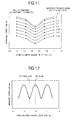
- the peak amplitude of the measured waveform is mostly increased when the inter-polarized channel delay time is n bit time (n is integer), whereas the peak amplitude of the measured waveform is mostly decreased when the inter-polarized channel delay time is (2n+1)/2 bit time.
- the inter-polarized channel delay time may be variably controlled in the optical signal stage thereof
- the direct current component in the electric signal obtained by photo-electrically converting the polarization interfering light is eliminated by the signal processing section 34, and the inter-polarized channel delay time is judged based on the change in the power of the alternate current component of which frequency band is restricted as needed.
- FIG. 23 is a block diagram illustrating a configuration of the polarization multiplexed light transmitter in the fourth embodiment.
- a synchronous detecting section 38 that extracts the frequency component at the baud rate (or the frequency component at n times the baud rate) from the electric signal output from the photoelectric conversion section 33, is disposed, so that the power of the frequency component extracted by the synchronous detecting section 38 is measured by the power measuring section 35 and a measurement result is transferred to the delay control section 36.
- other configurations in the fourth embodiment except for the synchronous detecting section 38 are same as those in the first embodiment, and accordingly, the description thereof is omitted here.
- the synchronous detecting section 38 is fed with a signal having a frequency corresponding to the baud rate (or n times the baud rate) of the modulation signal generated by each of the modulation driving sections 14A and 14B, and using this signal, synchronously detects the electric signal from the photoelectric conversion section 33 to extract the frequency component corresponding to the baud rate (or n times of the baud rate).
- a narrow band-pass filter which incudes the frequency corresponding the baud rate (or n times the baud rate) within a pass-band thereof, may be inserted between the photoelectric conversion section 33 and the synchronous detecting section 38 or may be disposed in place of the photoelectric conversion section 33.
- the inter-polarized channel delay time is judged based on the change in the power measured by the power measuring section 35.
- the frequency component surrounded by each broken line in calculation results illustrated in FIG. 24 is extracted by the synchronous detecting section 38.
- the power measured by the power measuring section 35 is the power obtained by combining a linear spectrum component at the baud rate (or n times the baud rate) with the frequency component in the vicinity thereof.
- the power measured by the power measuring section 35 is mostly increased when the inter-polarized channel delay time is 0 bit time, while being mostly decreased when the inter-polarized channel delay time is 1/2 bit time. Further, in the case where the frequency component corresponding to two times the baud rate is extracted, the power measured by the power measuring section 35 is mostly decreased when the inter-polarized channel delay time is 0 bit time, while being mostly increased when the inter-polarized channel delay time is 1/2 bit time. Incidentally, focusing on only the linear spectrum component of two times the baud rate, there is a feature in that the linear spectrum component is lost when the inter-polarized channel delay time is 1/4 bit time.
- the delay control section 36 may feedback control the delay amount varying sections 21A and 21B so that the measured power of the power measuring section 25 becomes minimal, whereas when the inter-polarized channel delay time is set to be bit-aligned, the delay control section 36 may feedback control the delay amount varying sections 21A and 21B so that the measured power of the power measuring section 25 becomes maximal.
- the delay control section 36 may feedback control the delay amount varying sections 21A and 21B in accordance with relations adverse to the above.
- the delay amount varying sections 21A and 21B are feedback controlled so that the linear spectrum component of two times the baud rate is lost, it becomes also possible to set the inter-polarized channel delay time to 1/4 bit time (an intermediate state between the bit interleave and the bit align).
- FIG. 25 is a block diagram illustrating a configuration of a practical example of the polarization multiplexed light transmitter corresponding to the fourth embodiment.
- a synchronous detecting circuit 381 is disposed, and in the synchronous detecting circuit 381, the frequency component corresponding to the baud rate (or n times the baud rate) is extracted from the electric signal output from the light receiving element 331, and further, the power of the frequency component is monitored by the power monitor 351.
- the fourth embodiment described above and the practical example thereof similarly to the first embodiment and the practical example 1-1, it is possible to effectively suppress the transmission characteristics degradation of the polarization multiplexed light due to the change in system state, by extracting the frequency component corresponding to the baud rate (or n times the baud rate) from the electric signal obtained by photo-electrically converting the polarization interfering light to control the inter-polarized channel delay time based on the change in the monitored power of the frequency component.
- the pulse timing between the polarized channels may be variably controlled in an optical signal stage thereof.
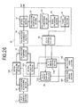
- FIG. 26 is a block diagram illustrating a configuration of the polarization multiplexed light transmitter in the fifth embodiment.
- a polarization scrambling section 39 is disposed on an optical path between the polarization combining section 15 and the optical branching section 31, and the polarization state of the polarization multiplexed light combined by the polarization combining section 15 fluctuates randomly by the polarization scrambling section 39.
- other configurations in the fifth embodiment except for the polarization scrambling section 39 are same as those in the first embodiment, and accordingly, the description thereof is omitted here.
- the delay control section 36 may feedback control the delay amount varying sections 21A and 21B so that the measured power becomes minimal, when the inter-polarized channel delay time is set to be bit-interleaved. Further, the delay control section 36 may feedback control the delay amount varying sections 21A and 21B so that the measured power becomes maximal, when the inter-polarized channel delay time is set to be bit-aligned.
- the polarization state of the polarization multiplexed light is varied randomly by the polarization scrabbling section 39. Therefore, since the polarization state of the monitor light does not need to be administrated when the orthogonal polarization channels in the monitor light are made to interfere with each other, it becomes possible to readily realize a monitoring system.
- the polarization scrambling section 39 is arranged between the polarization combining section 15 and the optical branching section 31.
- FIG. 28 it is possible to obtain a similar functional effect by disposing the polarization scrambling section 39 on an optical path between the branching port of the optical branching section 31 and the polarization interfering section 32.
- the polarization scrambling section 39 is disposed to the configuration of the first embodiment.
- the modulation format for the polarization multiplexed light in this invention is not limited to the above example.
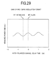
- the power of the alternate current component in the electric signal obtained by photo-electrically converting the polarization interfering light is measured for a signal light obtained by polarization multiplexing a NRZ-DQPSK modulated light of which pulsed format is different from that of the RZ-DQPSK modulated light, it can be verified that the change in the measured power indicates dependence, as illustrated in calculation results of FIG.
- the NRZ-DQPSK modulation format has dependence basically same as that of the RZ-DQPSK modulation format although the control sensitivity thereof is inferior to that of the RZ-DQPSK modulation format, and accordingly, it is understood that the inter-polarized channel delay time can be judged based on the change in the measured power.
Landscapes
- Physics & Mathematics (AREA)
- Engineering & Computer Science (AREA)
- Computer Networks & Wireless Communication (AREA)
- Signal Processing (AREA)
- Electromagnetism (AREA)
- Optics & Photonics (AREA)
- Nonlinear Science (AREA)
- Optical Communication System (AREA)
Applications Claiming Priority (1)
| Application Number | Priority Date | Filing Date | Title |
|---|---|---|---|
| JP2008232413A JP5083134B2 (ja) | 2008-09-10 | 2008-09-10 | 偏波多重光送信器およびその制御方法 |
Publications (2)
| Publication Number | Publication Date |
|---|---|
| EP2164199A2 true EP2164199A2 (fr) | 2010-03-17 |
| EP2164199A3 EP2164199A3 (fr) | 2012-04-25 |
Family
ID=41382427
Family Applications (1)
| Application Number | Title | Priority Date | Filing Date |
|---|---|---|---|
| EP09169702A Withdrawn EP2164199A3 (fr) | 2008-09-10 | 2009-09-08 | Transmetteur de lumière de polarisation multiplexée et son procédé de commande |
Country Status (3)
| Country | Link |
|---|---|
| US (1) | US8412047B2 (fr) |
| EP (1) | EP2164199A3 (fr) |
| JP (1) | JP5083134B2 (fr) |
Cited By (6)
| Publication number | Priority date | Publication date | Assignee | Title |
|---|---|---|---|---|
| EP2280498A1 (fr) * | 2009-07-28 | 2011-02-02 | Fujitsu Limited | Émetteur de signaux optiques et procédé de contrôle d'un signal optique multiplexé par polarisation |
| EP2385637A1 (fr) * | 2010-05-07 | 2011-11-09 | Telefonaktiebolaget L M Ericsson AB (Publ) | Procédés et dispositifs pour moduler un signal |
| WO2013045423A1 (fr) * | 2011-09-26 | 2013-04-04 | Alcatel Lucent | Procédé de génération de format de modulation pm inrz-xpsk |
| WO2014083800A1 (fr) * | 2012-11-27 | 2014-06-05 | 日本電気株式会社 | Emetteur de lumière multiplexé par polarisation et procédé de détermination de polarité |
| EP3029512A1 (fr) * | 2014-12-02 | 2016-06-08 | Xieon Networks S.à r.l. | Détection d'inversion spectrale pour transmission optique multiplexée à division de polarisation |
| EP2875599A4 (fr) * | 2012-07-20 | 2016-08-03 | Finisar Corp | Procede et appareil pour la stabilisation d'un emetteur optique |
Families Citing this family (48)
| Publication number | Priority date | Publication date | Assignee | Title |
|---|---|---|---|---|
| US9235100B1 (en) * | 2007-02-27 | 2016-01-12 | Celight | Apparatus for dual-polarization QAM and optical communications system using the same cross-reference to related application |
| JP5186993B2 (ja) * | 2008-04-30 | 2013-04-24 | 富士通株式会社 | 偏波多重光送受信装置 |
| JP5476697B2 (ja) | 2008-09-26 | 2014-04-23 | 富士通株式会社 | 光信号送信装置 |
| US9374188B2 (en) * | 2008-12-12 | 2016-06-21 | Alcatel Lucent | Optical communication using polarized transmit signal |
| JP2010199657A (ja) * | 2009-02-23 | 2010-09-09 | Oki Electric Ind Co Ltd | 時分割多重符号化送信信号生成方法及び時分割多重符号化送信信号生成装置 |
| US20120087653A1 (en) * | 2009-07-01 | 2012-04-12 | Mitsubishi Electric Corporation | Optical transmission apparatus and optical transmission method |
| US8811827B2 (en) * | 2009-09-25 | 2014-08-19 | Infinera Corporation | System for generating optical RZ signals based on electrical RZ signals |
| JP2011188213A (ja) * | 2010-03-08 | 2011-09-22 | Fujitsu Ltd | 光信号送信装置、光増幅装置、光減衰装置及び光信号送信方法 |
| JP5585190B2 (ja) | 2010-04-30 | 2014-09-10 | 富士通株式会社 | 光伝送システム,光送信装置,光受信装置及び光伝送方法 |
| US9054808B2 (en) * | 2010-10-08 | 2015-06-09 | Infinera Corporation | Controlled depolarization using chirp for mitigation of nonlinear polarization scattering |
| US8842997B2 (en) | 2011-01-06 | 2014-09-23 | Alcatel Lucent | Apparatus and method for generating interleaved return-to-zero (IRZ) polarization-division multiplexed (PDM) signals |
| EP2506478A1 (fr) * | 2011-03-25 | 2012-10-03 | Alcatel Lucent | Procédé de transmission optique de données utilisant le multiplexage de division de polarisation |
| CN102201868B (zh) * | 2011-04-06 | 2014-01-01 | 烽火通信科技股份有限公司 | 双并联mz调制器的偏置控制方法与装置 |
| US8873953B2 (en) * | 2011-06-17 | 2014-10-28 | Nec Laboratories America, Inc. | Multiple-symbol polarization switching for differential-detection modulation formats |
| CN102439887B (zh) * | 2011-10-18 | 2015-01-07 | 华为技术有限公司 | 信号调制装置和调制方法 |
| US20130177316A1 (en) * | 2012-01-06 | 2013-07-11 | Emcore Corporation | Optical communication system, and transmitter and receiver apparatus therefor |
| JP5877727B2 (ja) * | 2012-02-14 | 2016-03-08 | 日本オクラロ株式会社 | 半導体光変調素子及び光モジュール |
| JP5962455B2 (ja) * | 2012-11-21 | 2016-08-03 | 富士通株式会社 | 光伝送装置、ノード装置、光伝送方法および光伝送システム |
| US9407361B1 (en) * | 2012-12-12 | 2016-08-02 | Juniper Networks, Inc. | Minimizing polarization-dependent optical power for PM-M-QAM transmitters |
| TWI497927B (zh) * | 2013-12-31 | 2015-08-21 | Ind Tech Res Inst | 可見光通訊發射端裝置、接收裝置及可見光通訊系統 |
| US9853737B2 (en) * | 2014-02-05 | 2017-12-26 | Acacia Communications, Inc. | Bias control of nested Mach-Zehnder modulators for the generation of optical QAM signals |
| WO2016008662A1 (fr) * | 2014-07-17 | 2016-01-21 | Infibra Technologies S.R.L. | Procede et appareil pour mesurer une valeur physique distribuee d'un dispositif optique a l'essai |
| JP6661913B2 (ja) * | 2015-07-28 | 2020-03-11 | 富士通オプティカルコンポーネンツ株式会社 | 光モジュール、及びこれを用いた光送信機 |
| US9705592B1 (en) * | 2016-04-05 | 2017-07-11 | Infinera Corporation | In-service skew monitoring in a nested Mach-Zehnder modulator structure using pilot signals and balanced phase detection |
| US20180351317A1 (en) * | 2017-04-27 | 2018-12-06 | Analog Photonics LLC | On-chip optical gain circuits |
| JP7024234B2 (ja) * | 2017-07-18 | 2022-02-24 | 富士通株式会社 | 光送信機、及び光送信機の制御方法 |
| US11251878B2 (en) | 2018-02-07 | 2022-02-15 | Infinera Corporation | Independently routable digital subcarriers for optical communication networks |
| US11368228B2 (en) | 2018-04-13 | 2022-06-21 | Infinera Corporation | Apparatuses and methods for digital subcarrier parameter modifications for optical communication networks |
| US11095389B2 (en) | 2018-07-12 | 2021-08-17 | Infiriera Corporation | Subcarrier based data center network architecture |
| US11258528B2 (en) | 2019-09-22 | 2022-02-22 | Infinera Corporation | Frequency division multiple access optical subcarriers |
| US11095364B2 (en) | 2019-03-04 | 2021-08-17 | Infiriera Corporation | Frequency division multiple access optical subcarriers |
| US11336369B2 (en) | 2019-03-22 | 2022-05-17 | Infinera Corporation | Framework for handling signal integrity using ASE in optical networks |
| JP7239822B2 (ja) * | 2019-03-26 | 2023-03-15 | 日本電信電話株式会社 | 偏波多重光送受信回路 |
| US11418312B2 (en) | 2019-04-19 | 2022-08-16 | Infinera Corporation | Synchronization for subcarrier communication |
| US11838105B2 (en) | 2019-05-07 | 2023-12-05 | Infinera Corporation | Bidirectional optical communications |
| US11190291B2 (en) | 2019-05-14 | 2021-11-30 | Infinera Corporation | Out-of-band communication channel for subcarrier-based optical communication systems |
| US11088764B2 (en) * | 2019-05-14 | 2021-08-10 | Infinera Corporation | Out-of-band communication channel for sub-carrier-based optical communication systems |
| US11489613B2 (en) | 2019-05-14 | 2022-11-01 | Infinera Corporation | Out-of-band communication channel for subcarrier-based optical communication systems |
| US11239935B2 (en) * | 2019-05-14 | 2022-02-01 | Infinera Corporation | Out-of-band communication channel for subcarrier-based optical communication systems |
| US11476966B2 (en) | 2019-05-14 | 2022-10-18 | Infinera Corporation | Out-of-band communication channel for subcarrier-based optical communication systems |
| US11218220B2 (en) | 2019-05-14 | 2022-01-04 | Infinera Corporation | Out-of-band communication channel for subcarrier-based optical communication systems |
| US11296812B2 (en) | 2019-05-14 | 2022-04-05 | Infinera Corporation | Out-of-band communication channel for subcarrier-based optical communication systems |
| US11297005B2 (en) | 2019-09-05 | 2022-04-05 | Infiriera Corporation | Dynamically switching queueing schemes for network switches |
| US12580673B2 (en) | 2019-09-20 | 2026-03-17 | Infinera Corporation | Optical communication system transmitting and receiving optical subcarriers having different spectral widths and/or power values |
| WO2021072409A1 (fr) | 2019-10-10 | 2021-04-15 | Tulasi Veguru | Systèmes de commutateurs de réseaux pour réseaux de communications optiques |
| EP4042606A1 (fr) | 2019-10-10 | 2022-08-17 | Infinera Corporation | Protection et restauration à double trajet de sous-porteuse optique pour réseaux de communication optique |
| US12081269B2 (en) | 2019-10-10 | 2024-09-03 | Infinera Corporation | Hub-leaf laser synchronization |
| JP7823778B2 (ja) * | 2023-02-08 | 2026-03-04 | 日本電気株式会社 | 光通信システムにおける変調タイミング調整方法および装置 |
Citations (2)
| Publication number | Priority date | Publication date | Assignee | Title |
|---|---|---|---|---|
| JP2002344426A (ja) | 2001-05-18 | 2002-11-29 | Kansai Electric Power Co Inc:The | 偏光状態制御信号の送受信方法および送受信装置 |
| JP2008119011A (ja) | 1999-08-27 | 2008-05-29 | Tahitian Noni Internatl Inc | モリンダ・シトリフォリア食物繊維 |
Family Cites Families (8)
| Publication number | Priority date | Publication date | Assignee | Title |
|---|---|---|---|---|
| US5111322A (en) * | 1991-04-04 | 1992-05-05 | At&T Bell Laboratories | Polarization multiplexing device with solitons and method using same |
| US6654105B2 (en) * | 2000-03-06 | 2003-11-25 | Corning Applied Technologies Corporation | Cross-correlating PMD detector |
| CN100452690C (zh) | 2002-05-10 | 2009-01-14 | 诺基亚西门子通信有限责任两合公司 | 减少光偏振-多路信号的信号递降的方法和装置 |
| DE102004005718A1 (de) * | 2004-02-05 | 2005-08-25 | Siemens Ag | Verfahren zur optischen Übertragung eines Polarisations-Multiplexsignals |
| JP4328724B2 (ja) | 2005-01-17 | 2009-09-09 | 富士通株式会社 | 光波形測定装置および光波形測定方法 |
| JP4657860B2 (ja) * | 2005-09-16 | 2011-03-23 | 富士通株式会社 | 光送信装置および光通信システム |
| JP4678653B2 (ja) * | 2006-05-09 | 2011-04-27 | 富士通株式会社 | 光送信装置 |
| JP5186993B2 (ja) | 2008-04-30 | 2013-04-24 | 富士通株式会社 | 偏波多重光送受信装置 |
-
2008
- 2008-09-10 JP JP2008232413A patent/JP5083134B2/ja not_active Expired - Fee Related
-
2009
- 2009-09-04 US US12/585,156 patent/US8412047B2/en not_active Expired - Fee Related
- 2009-09-08 EP EP09169702A patent/EP2164199A3/fr not_active Withdrawn
Patent Citations (2)
| Publication number | Priority date | Publication date | Assignee | Title |
|---|---|---|---|---|
| JP2008119011A (ja) | 1999-08-27 | 2008-05-29 | Tahitian Noni Internatl Inc | モリンダ・シトリフォリア食物繊維 |
| JP2002344426A (ja) | 2001-05-18 | 2002-11-29 | Kansai Electric Power Co Inc:The | 偏光状態制御信号の送受信方法および送受信装置 |
Non-Patent Citations (1)
| Title |
|---|
| "1.6-b/s/Hz Spectrally Efficient Transmission Over 1700km of SSMF Using 40x85.6-Gb/s POLMUX-RZ-DOPSK", JOUMAL OF LIGHTWAVE TECHNOLOGY, vol. 25, no. 1, 2 January 2007 (2007-01-02), pages 222 - 232 |
Cited By (14)
| Publication number | Priority date | Publication date | Assignee | Title |
|---|---|---|---|---|
| EP2280498A1 (fr) * | 2009-07-28 | 2011-02-02 | Fujitsu Limited | Émetteur de signaux optiques et procédé de contrôle d'un signal optique multiplexé par polarisation |
| US8731409B2 (en) | 2009-07-28 | 2014-05-20 | Fujitsu Limited | Method for controlling polarization multiplexed optical signal |
| US8472810B2 (en) | 2009-07-28 | 2013-06-25 | Fujitsu Limited | Optical signal transmitter and method for controlling polarization multiplexed optical signal |
| US8649687B2 (en) | 2010-05-07 | 2014-02-11 | Telefonaktiebolaget L M Ericsson (Publ) | Methods and devices for modulating a signal |
| EP2385637A1 (fr) * | 2010-05-07 | 2011-11-09 | Telefonaktiebolaget L M Ericsson AB (Publ) | Procédés et dispositifs pour moduler un signal |
| WO2011139222A1 (fr) * | 2010-05-07 | 2011-11-10 | Telefonaktiebolaget Lm Ericsson (Publ) | Procédés et dispositifs de modulation de signal |
| WO2013045423A1 (fr) * | 2011-09-26 | 2013-04-04 | Alcatel Lucent | Procédé de génération de format de modulation pm inrz-xpsk |
| EP2579484A1 (fr) * | 2011-09-26 | 2013-04-10 | Alcatel Lucent | Procédé de génération de format de modulation pm iNRZ-xPSK |
| EP2875599A4 (fr) * | 2012-07-20 | 2016-08-03 | Finisar Corp | Procede et appareil pour la stabilisation d'un emetteur optique |
| US9692518B2 (en) | 2012-07-20 | 2017-06-27 | Finisar Corporation | Method and apparatus for stabilization of optical transmitter |
| WO2014083800A1 (fr) * | 2012-11-27 | 2014-06-05 | 日本電気株式会社 | Emetteur de lumière multiplexé par polarisation et procédé de détermination de polarité |
| EP3029512A1 (fr) * | 2014-12-02 | 2016-06-08 | Xieon Networks S.à r.l. | Détection d'inversion spectrale pour transmission optique multiplexée à division de polarisation |
| WO2016087538A1 (fr) * | 2014-12-02 | 2016-06-09 | Xieon Networks S.À R.L. | Détection d'inversion de spectre pour une transmission optique multiplexée par répartition en polarisation |
| US10038516B2 (en) | 2014-12-02 | 2018-07-31 | Xieon Networks S.A.R.L. | Spectral inversion detection for polarization-division multiplexed optical transmission |
Also Published As
| Publication number | Publication date |
|---|---|
| EP2164199A3 (fr) | 2012-04-25 |
| US20100067914A1 (en) | 2010-03-18 |
| JP2010068235A (ja) | 2010-03-25 |
| JP5083134B2 (ja) | 2012-11-28 |
| US8412047B2 (en) | 2013-04-02 |
Similar Documents
| Publication | Publication Date | Title |
|---|---|---|
| US8412047B2 (en) | Polarization multiplexed light transmitter and control method thereof | |
| JP5446586B2 (ja) | 偏波多重光送信器および偏波多重光信号の制御方法 | |
| JP5476697B2 (ja) | 光信号送信装置 | |
| US8693870B2 (en) | Control apparatus, polarization multiplexing light modulator, light transmitting apparatus, and method of controlling polarization multiplexing light modulator | |
| JP4108254B2 (ja) | 光送信器および光伝送システム | |
| JP3892326B2 (ja) | 光変調器の制御装置 | |
| EP2840444A2 (fr) | Appareil et procédé de contrôle d'un modulateur optique | |
| US8086109B2 (en) | Polarization multiplexed optical transmitting and receiving apparatus | |
| EP1760520B1 (fr) | Modulateur à déplacement de phase différentiel quadratique et méthode pour déterminer sa tension de commande | |
| US8483576B2 (en) | Driving method and driving apparatus for optical modulator, and optical transmitter using same | |
| EP1825612B1 (fr) | Procede et appareil de controle de polarisation et d'alignement dans un emetteur de signal optique | |
| US20060263097A1 (en) | Optical transmitting apparatus, optical receiving apparatus, and optical communication system comprising them | |
| US20230396339A1 (en) | Configurable intensity-modulation direct detection (imdd) optical transceivers | |
| US20140294402A1 (en) | Optical transmission apparatus, optical transmission method and program for optical transmission | |
| US9264142B2 (en) | RZ optical modulator and RZ optical modulation method | |
| WO2010035662A1 (fr) | Emetteur optique, récepteur optique et système de communication optique | |
| JP5207993B2 (ja) | 光伝送装置及び方法 | |
| US8811827B2 (en) | System for generating optical RZ signals based on electrical RZ signals | |
| Zhao et al. | 40G QPSK and DQPSK modulation | |
| US20040090665A1 (en) | Separating apparatus for time division multiplexed signal light, and optical receiving apparatus and optical transmission system using the same | |
| WO2013031786A1 (fr) | Circuit de réglage de phase, dispositif de transmission optique et procédé de réglage de phase | |
| JP2010226769A (ja) | 差分m位相偏移変調方式に対応した光受信器および光受信方法 |
Legal Events
| Date | Code | Title | Description |
|---|---|---|---|
| PUAI | Public reference made under article 153(3) epc to a published international application that has entered the european phase |
Free format text: ORIGINAL CODE: 0009012 |
|
| AK | Designated contracting states |
Kind code of ref document: A2 Designated state(s): AT BE BG CH CY CZ DE DK EE ES FI FR GB GR HR HU IE IS IT LI LT LU LV MC MK MT NL NO PL PT RO SE SI SK SM TR |
|
| AX | Request for extension of the european patent |
Extension state: AL BA RS |
|
| PUAL | Search report despatched |
Free format text: ORIGINAL CODE: 0009013 |
|
| AK | Designated contracting states |
Kind code of ref document: A3 Designated state(s): AT BE BG CH CY CZ DE DK EE ES FI FR GB GR HR HU IE IS IT LI LT LU LV MC MK MT NL NO PL PT RO SE SI SK SM TR |
|
| AX | Request for extension of the european patent |
Extension state: AL BA RS |
|
| RIC1 | Information provided on ipc code assigned before grant |
Ipc: H04J 14/06 20060101AFI20120320BHEP Ipc: H04B 10/155 20060101ALI20120320BHEP |
|
| 17P | Request for examination filed |
Effective date: 20120917 |
|
| 17Q | First examination report despatched |
Effective date: 20121018 |
|
| STAA | Information on the status of an ep patent application or granted ep patent |
Free format text: STATUS: THE APPLICATION IS DEEMED TO BE WITHDRAWN |
|
| 18D | Application deemed to be withdrawn |
Effective date: 20180118 |