EP2166426A2 - Taktbereitstellungsvorrichtung - Google Patents
Taktbereitstellungsvorrichtung Download PDFInfo
- Publication number
- EP2166426A2 EP2166426A2 EP09011728A EP09011728A EP2166426A2 EP 2166426 A2 EP2166426 A2 EP 2166426A2 EP 09011728 A EP09011728 A EP 09011728A EP 09011728 A EP09011728 A EP 09011728A EP 2166426 A2 EP2166426 A2 EP 2166426A2
- Authority
- EP
- European Patent Office
- Prior art keywords
- clock
- frequency
- unit
- determination unit
- modules
- Prior art date
- Legal status (The legal status is an assumption and is not a legal conclusion. Google has not performed a legal analysis and makes no representation as to the accuracy of the status listed.)
- Withdrawn
Links
Images


Classifications
-
- G—PHYSICS
- G06—COMPUTING OR CALCULATING; COUNTING
- G06F—ELECTRIC DIGITAL DATA PROCESSING
- G06F1/00—Details not covered by groups G06F3/00 - G06F13/00 and G06F21/00
- G06F1/04—Generating or distributing clock signals or signals derived directly therefrom
- G06F1/08—Clock generators with changeable or programmable clock frequency
-
- G—PHYSICS
- G06—COMPUTING OR CALCULATING; COUNTING
- G06F—ELECTRIC DIGITAL DATA PROCESSING
- G06F1/00—Details not covered by groups G06F3/00 - G06F13/00 and G06F21/00
- G06F1/04—Generating or distributing clock signals or signals derived directly therefrom
-
- G—PHYSICS
- G06—COMPUTING OR CALCULATING; COUNTING
- G06F—ELECTRIC DIGITAL DATA PROCESSING
- G06F1/00—Details not covered by groups G06F3/00 - G06F13/00 and G06F21/00
- G06F1/04—Generating or distributing clock signals or signals derived directly therefrom
- G06F1/10—Distribution of clock signals, e.g. skew
-
- G—PHYSICS
- G06—COMPUTING OR CALCULATING; COUNTING
- G06F—ELECTRIC DIGITAL DATA PROCESSING
- G06F1/00—Details not covered by groups G06F3/00 - G06F13/00 and G06F21/00
- G06F1/26—Power supply means, e.g. regulation thereof
- G06F1/32—Means for saving power
Definitions
- the present invention relates to a clock supply device that variably adjusts a frequency of a clock supplied to each module of a computer system, as needed.
- Japanese Unexamined Patent Application Publication No. 09-237132 discloses an idea of setting and adjusting a clock frequency at four levels depending on the load and heat generation of a CPU and the remaining capacity of a battery.
- Japanese Unexamined Patent Application Publication No. 09-237132 discloses a technique in which a flag indicating a busy state is set each time the CPU inputs/outputs or accesses a memory, and the number of flags is counted to recognize the number of idle states of the CPU, thereby detecting the load state of the CPU (see the paragraph [0017] of Japanese Unexamined Patent Application Publication No. 09-237132 ).
- the present inventor has found a problem that the granularity of the control is too coarse to estimate the load on the entire system by monitoring only the operation of the CPU, and many other modules constituting the system are not taken into consideration. This causes such inconveniences that the high-speed clock is unnecessarily supplied throughout the entire system, or the clock frequency is decreased even when some modules require high-speed operation.
- a polling operation is executed at predetermined cycles even when the CPU is in the idle state, and therefore, the input/output and the access to a memory are made all the time. This causes a problem that, even when the number of inputs/outputs and the number of memory access operations are counted, it is virtually impossible to estimate the real load on the CPU and the real load on the entire system with high precision.
- a first exemplary aspect of an embodiment of the present invention is a clock supply device that supplies a clock to a plurality of modules, including: a clock output unit that switches between clocks having different frequencies and output the clocks; a clock distribution unit that distributes and supplies the clocks from the clock output unit to the plurality of modules; and a clock switching control unit that causes the frequencies of the clocks from the clock output unit to be switched.
- the clock switching control unit includes a clock request pattern determination unit that outputs a control signal for decreasing a clock frequency to a slow frequency, to the clock output unit, when a pattern of a clock request signal output from a monitoring target module selected as a monitoring target from among the plurality of modules satisfies a predetermined condition pattern.
- the clock frequency is decreased to a slow frequency.
- the load on the system can be estimated with high precision.
- necessary tasks are executed appropriately, and power overhead can be minimized and power consumption can be reduced.
- a clock supply device according to a first exemplary embodiment of the present invention will be described.
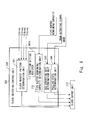
- Fig. 1 is a diagram showing the overall configuration of a computer system 100.
- the computer system 100 includes an operation execution unit 110 and a clock supply unit (clock supply device) 200.
- the operation execution unit 110 includes a central processing unit (CPU) 111, a digital signal processor (DSP) 112, a direct memory access controller (DMAC) 113, a graphic display controller (GDC) 114, a dynamic random access memory (DRAM) 115, and a bus 116 for connecting these components together.
- CPU central processing unit
- DSP digital signal processor
- DMAC direct memory access controller
- GDC graphic display controller
- DRAM dynamic random access memory
- bus 116 for connecting these components together.
- each of modules (111 to 115) mounted in the operation execution unit 110 requires a clock signal for providing a duty cycle. Accordingly, each of the modules (111 to 115) causes a clock request signal (Clkreq) to rise during the operation, and causes the clock request signal to fall during the time when the operation is stopped.
- a clock request signal (Clkreq)
- the clock supply unit 200 supplies a clock to the operation execution unit 110.
- the clock supply unit 200 includes a clock output unit 210, a clock distribution unit 220, a gate unit 230, and a clock switching control unit 240.
- the clock output unit 210 includes a PLL 211, a frequency division unit 212, and a switching unit 215.
- the PLL 211 multiplies a basic clock that is externally supplied, to thereby generate a high-speed clock.
- the frequency division unit 212 divides the frequency of the high-speed clock from the PLL 211 at a predetermined frequency dividing rate.
- the frequency division unit 212 includes a divide-by-16 frequency division unit 213 for dividing the frequency of the high-speed clock from the PLL 211 by 16 to thereby obtain a low-speed clock, and a divide-by-2 frequency division unit 214 for dividing the frequency of the clock by 2 to thereby obtain a medium-speed clock.
- the switching unit 215 switches between the high-speed clock from the PLL 211 and the low-speed clock from the frequency division unit 212, and outputs the clocks.
- the switching unit 215 performs switching control in response to a control signal from the clock switching control unit 240.
- the clock distribution unit 220 receives a clock signal from the clock output unit 210. Then, the clock distribution unit 220 generates a plurality of clocks to be distributed to the modules (111 to 115) in synchronization with the received clock, and outputs the plurality of clock signals.
- the gate unit 230 includes a plurality of AND circuits.
- the AND circuits are provided to respectively correspond to the modules (111 to 115).
- Each of the AND circuits receives the clock request signal from each of the modules (111 to 115), and the other input of each of the AND circuits receives the clock signal from the clock distribution unit 220.
- the clock switching control unit 240 includes a clock request pattern determination unit 241, a FIFO buffer remaining capacity determination unit 242, a bus operation rate determination unit 243, and a polling state determination unit 244.
- the clock request pattern determination unit 241 receives the clock request signal Clkreq from each of the modules (111 to 115).
- the clock request pattern determination unit 241 monitors the presence or absence of the clock request from each of the modules (111 to 115), and compares a pattern indicating the presence or absence of the clock request with a predetermined condition pattern.
- the clock request pattern determination unit 241 is provided with a condition setting register 241A.
- the condition setting register 241A has registered therein in advance the identification codes of the plurality of modules (111 to 115), and is configured to be able to selectively set a module to be monitored.
- Fig. 2 is a table showing a configuration example of the condition setting register 241A.
- the condition setting register 241A has module names registered therein, and is configured to be able to arbitrarily set a monitoring flag to "0" or "1".
- the monitoring flag is set to "0" as an initial value.
- the module is set as a monitoring target, and when the monitoring flag is set to "1 ", the module can be selectively set to be excluded from the monitoring target.
- the clock request pattern determination unit 241 determines that the condition is satisfied, and outputs a control signal for dividing the clock frequency by 16.
- the FIFO buffer remaining capacity determination unit 242 monitors the FIFO buffer remaining capacity of a FIFO type module that processes data in order from the top.
- the FIFO buffer remaining capacity determination unit 242 has a threshold set therein. When the value of the FIFO buffer remaining capacity exceeds the threshold, the FIFO buffer remaining capacity determination unit 242 determines that the value of the FIFO buffer remaining capacity is within a safe zone, and outputs a control signal for dividing the clock frequency by 16.
- the graphic display controller (GDC) 114 is one example of the FIFO type module.
- the clock request signal Clkreq from the graphic display controller (GDC) 114 is not input to the clock request pattern determination unit 241, but the value of the FIFO buffer remaining capacity is monitored by the FIFO buffer remaining capacity determination unit 242.
- the determination result from the clock request pattern determination unit 241 and the determination result from the FIFO buffer remaining capacity determination unit 242 are further determined by an AND circuit 245 under an AND condition. When both conditions are satisfied, a switching control signal for causing a divided-by-16 clock, i.e., the lowest-speed clock to be output is supplied to the clock output unit 210.
- the clock output unit 210 Upon receiving the switching control signal, the clock output unit 210 generates a divided-by-16 clock using the frequency division unit 212, and the switching unit 215 performs switching operation to cause the divided-by-16 clock from the frequency division unit 212 to be output.
- the bus operation rate determination unit 243 monitors the operation rate of the bus 116, and controls the clock frequency to be increased, maintained, or decreased according to the operation rate of the bus 116 per unit time.
- the bus operation rate determination unit 243 receives a signal for detecting an active state of each of an address bus and a data bus of the bus 116.
- the bus operation rate is estimated based on an active time of the DRAM 115 per unit time.
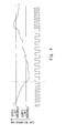
- Fig. 3 is a timing diagram showing operation timing of the DRAM 115.
- the active time of the DRAM 115 is defined as a time period from the input of an address, i.e., the start of a protocol, until the end of data, i.e., the end of the protocol.
- a ratio of the active time to the unit time is obtained, and the ratio thus obtained is used as the bus operation rate.
- the bus operation rate determination unit 243 has set therein an upper-limit threshold and a lower-limit threshold, and compares the bus operation rate with the upper-limit threshold and the lower-limit threshold, to thereby determine the increase and decrease of the clock frequency.
- Fig. 4 is a timing diagram showing a relationship between the bus operation rate and the clock frequency.
- a switching control signal for decreasing the clock frequency to a divided-by-2 frequency is output to the clock output unit 210.
- a switching signal for increasing the clock frequency to a divided-by-1 frequency namely, setting the clock frequency to the fastest frequency.
- the polling state determination unit 244 monitors the address bus of the bus 116 to detect a module in a polling state, and compares the detected module with the predetermined condition, thereby controlling the clock frequency to be increased or decreased.
- the polling state determination unit 244 monitors an address signal from the address bus. When the same address is output a predetermined number of times (e.g., three times) in succession, the polling state determination unit 244 determines that the module has entered the polling state.
- the CPU 111 and the DSP 112 are herein described as examples of polling monitoring targets.
- the polling state determination unit 244 supplies the clock output unit 210 with a control signal for decreasing the clock frequency to a divided-by-2 frequency.
- the polling state determination unit 244 determines whether the other of the CPU 111 and the DSP 112 is in a stand-by state. Then, when the other of the CPU 111 and the DSP 112 is in the stand-by state, the polling state determination unit 244 supplies the clock output unit 210 with a control signal for dividing the clock frequency by 2.
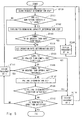
- Fig. 5 is a flowchart showing an operation procedure of a clock frequency control method carried out by the clock supply unit 200.
- the clock having the fastest frequency i.e., divided-by-1 frequency from PLL
- the clock output unit 210 the clock having the fastest frequency (i.e., divided-by-1 frequency from PLL) is output from the clock output unit 210.
- the clock request pattern determination unit 241 compares the presence or absence of the clock request from each of the modules (111 to 115) with the condition set in the condition setting register 241A, and determines whether all the clock request signals from the monitoring target modules are at "L" level.
- the FIFO buffer remaining capacity determination unit 242 When it is determined that all the clock request signals from the monitoring target modules are at "L" level (YES in ST101), the FIFO buffer remaining capacity determination unit 242 then carries out a FIFO buffer remaining capacity determination step (ST102).
- the FIFO buffer remaining capacity of the FIFO type module (e.g., GDC) to be monitored is compared with a safety threshold.
- the FIFO buffer remaining capacity of the FIFO type module e.g., GDC
- the process returns to ST100 to repeat the loop.
- the divided-by-16 clock i.e., the lowest-speed clock is continuously supplied.
- the bus operation rate is measured based on the active time of the DRAM 115 per unit time, and the bus operation rate is compared with the threshold (lower-limit threshold, upper-limit threshold).
- the predetermined condition of the clock request determination step (ST100) or the FIFO buffer remaining capacity determination step (ST102) is not satisfied (NO in ST101 and ST103).
- the clock frequency is divided by 2 to obtain a medium-speed frequency.
- a control signal for dividing the clock frequency by 1 is supplied to the clock output unit 210 (ST111). That is, the clock frequency is increased.
- the flow of the task processing of each module is interrupted and a large number of modules access the DRAM 115 without interruption, which results in an increase in bus operation rate.
- the clock frequency is increased to the fastest frequency.
- the clock frequency is increased to thereby cause the operation execution unit 110 to rapidly execute the necessary processing at necessary timing.
- bus operation rate determination step (ST104) when the bus operation rate falls between the upper-limit threshold and the lower-limit threshold (NO in ST105 and ST106), the clock frequency is maintained as it is, and then a polling determination step (ST107) is carried out.
- an address signal from an address bus is monitored to determine whether a monitoring target module (e.g., CPU, DSP) that is outputting the same address a predetermined number of times (e.g., three times) in succession is present.
- a monitoring target module e.g., CPU, DSP
- a control signal for dividing the clock frequency by 2 is supplied to the clock output unit 210 (ST110).
- the clock frequency is divided by 2 to obtain the medium-speed frequency.
- the clock frequency is restored to the divided-by-1 frequency, i.e., the fastest frequency.
- the process returns to ST100 to repeat the loop until a termination condition (ST112) is satisfied.
- the termination condition is satisfied when an instruction for stopping the system is input, for example.
- Fig. 6 is a diagram showing the configuration of the first modification.
- the determination results of each of the clock request pattern determination unit 241 and the FIFO buffer remaining capacity determination unit 242 are determined under the AND condition, and when both conditions are satisfied, the clock frequency is divided by 16.
- the determination results of the clock request pattern determination unit 241 and a FIFO buffer remaining capacity determining unit 310 are not necessarily determined under the AND condition as shown in Fig. 6 .
- each of the clock request pattern determination unit 241 and the FIFO buffer remaining capacity determining unit 310 supplies a control signal to the clock output unit 210 without involving any AND circuit.
- the FIFO buffer remaining capacity determining unit 310 has not only the safety threshold but also a risk threshold set therein.
- Fig. 7 is a timing diagram showing a relationship between the FIFO buffer remaining capacity and the clock frequency.
- a switching control signal for dividing the clock frequency by 1 is supplied to the clock output unit 210. That is, the switching signal for increasing the clock frequency to the fastest frequency is output.
- the clock frequency is divided by 2.
- Fig. 8 is a flowchart showing an operation procedure of the first modification.
- the clock request pattern determination unit 241 supplies the clock output unit 210 with a control signal for dividing the clock frequency by 16.
- the FIFO buffer remaining capacity determination step (ST102) is carried out, and the FIFO buffer remaining capacity of the FIFO type module (e.g., GDC) to be monitored is compared with the safety threshold and the risk threshold.
- the FIFO buffer remaining capacity of the FIFO type module e.g., GDC
- the clock frequency is divided by 1.
- the bus operation rate is estimated based on the active time of the DRAM, but the method of estimating the bus operation rate is not limited thereto and other methods capable of estimating the bus operation rate (i.e., an amount of traffic on the bus) may be employed.
- the clock output unit outputs not only the highest-speed clock from the PLL but also the divided-by-16 clock, i.e., the lowest-speed clock, and the divided-by-2 clock, i.e., the medium-speed clock.
- the frequency dividing rate of the frequency division unit may be divided into more detailed levels.
- the threshold is broken down into multiple levels, and the multiple levels of thresholds may be set in each of the FIFO buffer remaining capacity determination unit and the bus operation rate determination unit. Furthermore, the clock frequency may be selected at more detailed levels corresponding to the thresholds.
- Fig. 3 illustrates the operation of a synchronous DRAM as an example of a DRAM operation
- the protocol for reading out data from the DRAM such as a random access mode or a fast page mode, varies depending on the DRAM from which data is read out.
Landscapes
- Engineering & Computer Science (AREA)
- Theoretical Computer Science (AREA)
- Physics & Mathematics (AREA)
- General Engineering & Computer Science (AREA)
- General Physics & Mathematics (AREA)
- Information Transfer Systems (AREA)
- Power Sources (AREA)
Applications Claiming Priority (1)
| Application Number | Priority Date | Filing Date | Title |
|---|---|---|---|
| JP2008238953A JP2010072897A (ja) | 2008-09-18 | 2008-09-18 | クロック供給装置 |
Publications (1)
| Publication Number | Publication Date |
|---|---|
| EP2166426A2 true EP2166426A2 (de) | 2010-03-24 |
Family
ID=41180860
Family Applications (1)
| Application Number | Title | Priority Date | Filing Date |
|---|---|---|---|
| EP09011728A Withdrawn EP2166426A2 (de) | 2008-09-18 | 2009-09-14 | Taktbereitstellungsvorrichtung |
Country Status (5)
| Country | Link |
|---|---|
| US (1) | US20100070793A1 (de) |
| EP (1) | EP2166426A2 (de) |
| JP (1) | JP2010072897A (de) |
| KR (1) | KR101108898B1 (de) |
| CN (1) | CN101676831A (de) |
Cited By (1)
| Publication number | Priority date | Publication date | Assignee | Title |
|---|---|---|---|---|
| US20220383911A1 (en) * | 2021-05-25 | 2022-12-01 | Yangtze Memory Technologies Co., Ltd. | Method and apparatus for power saving in semiconductor devices |
Families Citing this family (6)
| Publication number | Priority date | Publication date | Assignee | Title |
|---|---|---|---|---|
| CN103095739A (zh) * | 2011-10-27 | 2013-05-08 | 英业达科技有限公司 | 机柜服务器系统及其节点通信方法 |
| JP6774160B2 (ja) * | 2013-12-06 | 2020-10-21 | キヤノン株式会社 | 情報処理装置、並びに、データ転送装置の制御方法 |
| CN105353827A (zh) * | 2014-08-22 | 2016-02-24 | 中兴通讯股份有限公司 | 一种控制方法、装置及功能板 |
| US9660799B1 (en) * | 2015-11-24 | 2017-05-23 | Intel Corporation | Changing the clock frequency of a computing device |
| KR102576707B1 (ko) * | 2016-12-26 | 2023-09-08 | 삼성전자주식회사 | 전자 시스템 및 그 동작 방법 |
| CN114721899B (zh) * | 2022-03-18 | 2024-09-06 | 山东方寸微电子科技有限公司 | 一种可变时钟频率检测电路及其工作方法 |
Citations (2)
| Publication number | Priority date | Publication date | Assignee | Title |
|---|---|---|---|---|
| JPH09237132A (ja) | 1996-02-29 | 1997-09-09 | Toshiba Corp | コンピュータシステム及びそのクロック制御方法 |
| JP2005250650A (ja) | 2004-03-02 | 2005-09-15 | Nec Electronics Corp | マルチレイヤシステム及びクロック制御方法 |
Family Cites Families (14)
| Publication number | Priority date | Publication date | Assignee | Title |
|---|---|---|---|---|
| JPH10232853A (ja) * | 1997-02-18 | 1998-09-02 | Toshiba Corp | シリアルデータ転送回路 |
| WO2000002118A1 (fr) * | 1998-07-02 | 2000-01-13 | Hitachi, Ltd. | Microprocesseur |
| US6564329B1 (en) * | 1999-03-16 | 2003-05-13 | Linkup Systems Corporation | System and method for dynamic clock generation |
| US6636976B1 (en) * | 2000-06-30 | 2003-10-21 | Intel Corporation | Mechanism to control di/dt for a microprocessor |
| JP3852703B2 (ja) * | 2001-08-29 | 2006-12-06 | アナログ・デバイシズ・インコーポレーテッド | 無線システムにおけるタイミングおよび事象処理の方法および装置 |
| GB0123421D0 (en) * | 2001-09-28 | 2001-11-21 | Memquest Ltd | Power management system |
| US6978389B2 (en) * | 2001-12-20 | 2005-12-20 | Texas Instruments Incorporated | Variable clocking in an embedded symmetric multiprocessor system |
| US7051227B2 (en) * | 2002-09-30 | 2006-05-23 | Intel Corporation | Method and apparatus for reducing clock frequency during low workload periods |
| US7640446B1 (en) * | 2003-09-29 | 2009-12-29 | Marvell International Ltd. | System-on-chip power reduction through dynamic clock frequency |
| US7325152B2 (en) * | 2005-06-30 | 2008-01-29 | Infineon Technologies Ag | Synchronous signal generator |
| JP2007058279A (ja) * | 2005-08-22 | 2007-03-08 | Oki Electric Ind Co Ltd | パワーダウン移行システム |
| US20070260771A1 (en) * | 2006-04-10 | 2007-11-08 | Cheng-Hao Lee | Method of Reducing Clock Differential in a Data Processing System |
| US7734941B2 (en) * | 2006-08-31 | 2010-06-08 | Ati Technologies Ulc | Power management scheme employing an indicator of a current device operating configuration that requires a minimum processing power |
| JP5231800B2 (ja) * | 2007-12-26 | 2013-07-10 | 株式会社東芝 | 半導体集積回路装置および半導体集積回路装置のクロック制御方法 |
-
2008
- 2008-09-18 JP JP2008238953A patent/JP2010072897A/ja not_active Withdrawn
-
2009
- 2009-09-11 US US12/585,337 patent/US20100070793A1/en not_active Abandoned
- 2009-09-14 EP EP09011728A patent/EP2166426A2/de not_active Withdrawn
- 2009-09-17 KR KR1020090088077A patent/KR101108898B1/ko not_active Expired - Fee Related
- 2009-09-18 CN CN200910173461A patent/CN101676831A/zh active Pending
Patent Citations (2)
| Publication number | Priority date | Publication date | Assignee | Title |
|---|---|---|---|---|
| JPH09237132A (ja) | 1996-02-29 | 1997-09-09 | Toshiba Corp | コンピュータシステム及びそのクロック制御方法 |
| JP2005250650A (ja) | 2004-03-02 | 2005-09-15 | Nec Electronics Corp | マルチレイヤシステム及びクロック制御方法 |
Cited By (3)
| Publication number | Priority date | Publication date | Assignee | Title |
|---|---|---|---|---|
| US20220383911A1 (en) * | 2021-05-25 | 2022-12-01 | Yangtze Memory Technologies Co., Ltd. | Method and apparatus for power saving in semiconductor devices |
| US11967393B2 (en) * | 2021-05-25 | 2024-04-23 | Yangtze Memory Technologies Co., Ltd. | Method and apparatus for power saving in semiconductor devices |
| US12327601B2 (en) | 2021-05-25 | 2025-06-10 | Yangtze Memory Technologies Co., Ltd. | Method and apparatus for power saving in semiconductor devices |
Also Published As
| Publication number | Publication date |
|---|---|
| JP2010072897A (ja) | 2010-04-02 |
| CN101676831A (zh) | 2010-03-24 |
| KR20100032838A (ko) | 2010-03-26 |
| US20100070793A1 (en) | 2010-03-18 |
| KR101108898B1 (ko) | 2012-01-30 |
Similar Documents
| Publication | Publication Date | Title |
|---|---|---|
| EP2166426A2 (de) | Taktbereitstellungsvorrichtung | |
| EP0451661B1 (de) | Mikroprozessor mit niedrigem Leistungsverbrauch | |
| KR101740338B1 (ko) | 디지털 시스템에서 동적 클럭 제어 장치 및 방법 | |
| US10585448B2 (en) | Low power autonomous peripheral management | |
| EP3451122B1 (de) | Leistungsverwaltung in einer integrierten schaltung | |
| US8695008B2 (en) | Method and system for dynamically controlling power to multiple cores in a multicore processor of a portable computing device | |
| US20110022833A1 (en) | Altering performance of computational units heterogeneously according to performance sensitivity | |
| US20110022857A1 (en) | Throttling computational units according to performance sensitivity | |
| EP3440531B1 (de) | Verbessertes schema für dynamische takt- und spannungsskalierung (dcvs) | |
| CN1312546C (zh) | 动态电压转变 | |
| TW201403299A (zh) | 中央處理器控制方法 | |
| EP2457139A1 (de) | Heterogene veränderung der leistung von rechnereinheiten je nach leistungssensitivität | |
| US8566493B2 (en) | Interrupt controller and methods of operation | |
| JP2015079496A (ja) | チップ上のマルチコアシステムの全域チップ電力を管理する方法およびその装置。 | |
| CN101403982A (zh) | 一种多核处理器的任务分配方法、系统及设备 | |
| US20110022356A1 (en) | Determining performance sensitivities of computational units | |
| JP6418056B2 (ja) | 演算処理装置及び演算処理装置の制御方法 | |
| TWI502332B (zh) | 電源管理方法及應用該方法之電子系統 | |
| CN101271387B (zh) | 数据缓存器溢出的自动解除方法和装置 | |
| US9448617B2 (en) | Systems and methods for messaging-based fine granularity system-on-a-chip power gating | |
| JP2011223179A (ja) | クロック発生回路及びその制御方法 | |
| JP2006331107A (ja) | 電力管理回路、及び電子回路 | |
| US8479034B2 (en) | Controlling the power usage of a computer | |
| JP2011013914A (ja) | 省電力制御装置、および省電力制御方法 | |
| JP4798445B2 (ja) | 省電力制御方法、画像形成装置およびプログラム |
Legal Events
| Date | Code | Title | Description |
|---|---|---|---|
| PUAI | Public reference made under article 153(3) epc to a published international application that has entered the european phase |
Free format text: ORIGINAL CODE: 0009012 |
|
| AK | Designated contracting states |
Kind code of ref document: A2 Designated state(s): AT BE BG CH CY CZ DE DK EE ES FI FR GB GR HR HU IE IS IT LI LT LU LV MC MK MT NL NO PL PT RO SE SI SK SM TR |
|
| AX | Request for extension of the european patent |
Extension state: AL BA RS |
|
| RAP1 | Party data changed (applicant data changed or rights of an application transferred) |
Owner name: RENESAS ELECTRONICS CORPORATION |
|
| STAA | Information on the status of an ep patent application or granted ep patent |
Free format text: STATUS: THE APPLICATION HAS BEEN WITHDRAWN |
|
| 18W | Application withdrawn |
Effective date: 20120830 |