EP2172965A1 - Procédé de mesure de caractéristique optique, procédé d'ajustement de caractéristique optique, dispositif d'exposition, procédé d'exposition, et procédé de fabrication de dispositif d'exposition - Google Patents
Procédé de mesure de caractéristique optique, procédé d'ajustement de caractéristique optique, dispositif d'exposition, procédé d'exposition, et procédé de fabrication de dispositif d'exposition Download PDFInfo
- Publication number
- EP2172965A1 EP2172965A1 EP08777560A EP08777560A EP2172965A1 EP 2172965 A1 EP2172965 A1 EP 2172965A1 EP 08777560 A EP08777560 A EP 08777560A EP 08777560 A EP08777560 A EP 08777560A EP 2172965 A1 EP2172965 A1 EP 2172965A1
- Authority
- EP
- European Patent Office
- Prior art keywords
- pattern
- optical characteristic
- optical system
- light
- image
- Prior art date
- Legal status (The legal status is an assumption and is not a legal conclusion. Google has not performed a legal analysis and makes no representation as to the accuracy of the status listed.)
- Withdrawn
Links
Images




Classifications
-
- G—PHYSICS
- G03—PHOTOGRAPHY; CINEMATOGRAPHY; ANALOGOUS TECHNIQUES USING WAVES OTHER THAN OPTICAL WAVES; ELECTROGRAPHY; HOLOGRAPHY
- G03F—PHOTOMECHANICAL PRODUCTION OF TEXTURED OR PATTERNED SURFACES, e.g. FOR PRINTING, FOR PROCESSING OF SEMICONDUCTOR DEVICES; MATERIALS THEREFOR; ORIGINALS THEREFOR; APPARATUS SPECIALLY ADAPTED THEREFOR
- G03F7/00—Photomechanical, e.g. photolithographic, production of textured or patterned surfaces, e.g. printing surfaces; Materials therefor, e.g. comprising photoresists; Apparatus specially adapted therefor
- G03F7/70—Microphotolithographic exposure; Apparatus therefor
- G03F7/708—Construction of apparatus, e.g. environment aspects, hygiene aspects or materials
- G03F7/7085—Detection arrangement, e.g. detectors of apparatus alignment possibly mounted on wafers, exposure dose, photo-cleaning flux, stray light, thermal load
-
- G—PHYSICS
- G01—MEASURING; TESTING
- G01M—TESTING STATIC OR DYNAMIC BALANCE OF MACHINES OR STRUCTURES; TESTING OF STRUCTURES OR APPARATUS, NOT OTHERWISE PROVIDED FOR
- G01M11/00—Testing of optical apparatus; Testing structures by optical methods not otherwise provided for
- G01M11/02—Testing optical properties
- G01M11/0242—Testing optical properties by measuring geometrical properties or aberrations
- G01M11/0257—Testing optical properties by measuring geometrical properties or aberrations by analyzing the image formed by the object to be tested
- G01M11/0264—Testing optical properties by measuring geometrical properties or aberrations by analyzing the image formed by the object to be tested by using targets or reference patterns
-
- G—PHYSICS
- G03—PHOTOGRAPHY; CINEMATOGRAPHY; ANALOGOUS TECHNIQUES USING WAVES OTHER THAN OPTICAL WAVES; ELECTROGRAPHY; HOLOGRAPHY
- G03F—PHOTOMECHANICAL PRODUCTION OF TEXTURED OR PATTERNED SURFACES, e.g. FOR PRINTING, FOR PROCESSING OF SEMICONDUCTOR DEVICES; MATERIALS THEREFOR; ORIGINALS THEREFOR; APPARATUS SPECIALLY ADAPTED THEREFOR
- G03F1/00—Originals for photomechanical production of textured or patterned surfaces, e.g., masks, photo-masks, reticles; Mask blanks or pellicles therefor; Containers specially adapted therefor; Preparation thereof
- G03F1/38—Masks having auxiliary features, e.g. special coatings or marks for alignment or testing; Preparation thereof
- G03F1/44—Testing or measuring features, e.g. grid patterns, focus monitors, sawtooth scales or notched scales
-
- G—PHYSICS
- G03—PHOTOGRAPHY; CINEMATOGRAPHY; ANALOGOUS TECHNIQUES USING WAVES OTHER THAN OPTICAL WAVES; ELECTROGRAPHY; HOLOGRAPHY
- G03F—PHOTOMECHANICAL PRODUCTION OF TEXTURED OR PATTERNED SURFACES, e.g. FOR PRINTING, FOR PROCESSING OF SEMICONDUCTOR DEVICES; MATERIALS THEREFOR; ORIGINALS THEREFOR; APPARATUS SPECIALLY ADAPTED THEREFOR
- G03F1/00—Originals for photomechanical production of textured or patterned surfaces, e.g., masks, photo-masks, reticles; Mask blanks or pellicles therefor; Containers specially adapted therefor; Preparation thereof
- G03F1/62—Pellicles, e.g. pellicle assemblies, e.g. having membrane on support frame; Preparation thereof
-
- G—PHYSICS
- G03—PHOTOGRAPHY; CINEMATOGRAPHY; ANALOGOUS TECHNIQUES USING WAVES OTHER THAN OPTICAL WAVES; ELECTROGRAPHY; HOLOGRAPHY
- G03F—PHOTOMECHANICAL PRODUCTION OF TEXTURED OR PATTERNED SURFACES, e.g. FOR PRINTING, FOR PROCESSING OF SEMICONDUCTOR DEVICES; MATERIALS THEREFOR; ORIGINALS THEREFOR; APPARATUS SPECIALLY ADAPTED THEREFOR
- G03F7/00—Photomechanical, e.g. photolithographic, production of textured or patterned surfaces, e.g. printing surfaces; Materials therefor, e.g. comprising photoresists; Apparatus specially adapted therefor
- G03F7/70—Microphotolithographic exposure; Apparatus therefor
- G03F7/70483—Information management; Active and passive control; Testing; Wafer monitoring, e.g. pattern monitoring
- G03F7/70605—Workpiece metrology
- G03F7/70616—Monitoring the printed patterns
- G03F7/70641—Focus
-
- G—PHYSICS
- G03—PHOTOGRAPHY; CINEMATOGRAPHY; ANALOGOUS TECHNIQUES USING WAVES OTHER THAN OPTICAL WAVES; ELECTROGRAPHY; HOLOGRAPHY
- G03F—PHOTOMECHANICAL PRODUCTION OF TEXTURED OR PATTERNED SURFACES, e.g. FOR PRINTING, FOR PROCESSING OF SEMICONDUCTOR DEVICES; MATERIALS THEREFOR; ORIGINALS THEREFOR; APPARATUS SPECIALLY ADAPTED THEREFOR
- G03F7/00—Photomechanical, e.g. photolithographic, production of textured or patterned surfaces, e.g. printing surfaces; Materials therefor, e.g. comprising photoresists; Apparatus specially adapted therefor
- G03F7/70—Microphotolithographic exposure; Apparatus therefor
- G03F7/70483—Information management; Active and passive control; Testing; Wafer monitoring, e.g. pattern monitoring
- G03F7/70605—Workpiece metrology
- G03F7/706843—Metrology apparatus
- G03F7/706849—Irradiation branch, e.g. optical system details, illumination mode or polarisation control
-
- G—PHYSICS
- G03—PHOTOGRAPHY; CINEMATOGRAPHY; ANALOGOUS TECHNIQUES USING WAVES OTHER THAN OPTICAL WAVES; ELECTROGRAPHY; HOLOGRAPHY
- G03F—PHOTOMECHANICAL PRODUCTION OF TEXTURED OR PATTERNED SURFACES, e.g. FOR PRINTING, FOR PROCESSING OF SEMICONDUCTOR DEVICES; MATERIALS THEREFOR; ORIGINALS THEREFOR; APPARATUS SPECIALLY ADAPTED THEREFOR
- G03F7/00—Photomechanical, e.g. photolithographic, production of textured or patterned surfaces, e.g. printing surfaces; Materials therefor, e.g. comprising photoresists; Apparatus specially adapted therefor
- G03F7/70—Microphotolithographic exposure; Apparatus therefor
- G03F7/70483—Information management; Active and passive control; Testing; Wafer monitoring, e.g. pattern monitoring
- G03F7/70605—Workpiece metrology
- G03F7/706843—Metrology apparatus
- G03F7/706851—Detection branch, e.g. detector arrangements, polarisation control, wavelength control or dark/bright field detection
-
- H—ELECTRICITY
- H10—SEMICONDUCTOR DEVICES; ELECTRIC SOLID-STATE DEVICES NOT OTHERWISE PROVIDED FOR
- H10P—GENERIC PROCESSES OR APPARATUS FOR THE MANUFACTURE OR TREATMENT OF DEVICES COVERED BY CLASS H10
- H10P76/00—Manufacture or treatment of masks on semiconductor bodies, e.g. by lithography or photolithography
- H10P76/20—Manufacture or treatment of masks on semiconductor bodies, e.g. by lithography or photolithography of masks comprising organic materials
- H10P76/204—Manufacture or treatment of masks on semiconductor bodies, e.g. by lithography or photolithography of masks comprising organic materials of organic photoresist masks
- H10P76/2045—Electron beam lithography processes
Definitions
- the present invention relates to an optical characteristic measuring method for measuring an optical characteristic of an optical system usable to produce an electronic device including, for example, semiconductor elements, liquid crystal display elements, etc. in the lithography step; an optical characteristic adjusting method for adjusting the optical characteristic of the optical system; an exposure apparatus provided with the optical system; an exposure method using the exposure apparatus; and an exposure apparatus producing method for producing the exposure apparatus.
- an exposure apparatus is used to expose a substrate (a glass plate, a semiconductor wafer, etc.) coated with a resist via an optical system (projection optical system) with a pattern formed on a mask (a reticle, a photomask, etc.). It is necessary for the exposure apparatus to project the pattern formed on the mask onto the substrate at a high resolution. Therefore, the optical system, which is provided on the exposure apparatus, is designed to have satisfactory optical characteristics in which various aberrations are sufficiently corrected.
- Japanese Patent Application Laid-open No. 2000-77295 describes a technique for measuring an optical characteristic of an optical system, wherein a spatial image of a phase pattern formed via the optical system is detected at a plurality of defocus positions to measure and determine the optical characteristic of the optical system based on the change of the intensity distribution of the detected spatial image of the phase pattern.
- the intensity distribution of the spatial image of the phase pattern is obtained by directly detecting the spatial image of the phase pattern formed via the optical system by, for example, a sensor such as CCD or the like.
- the sensor has a spatial resolution required to detect the intensity distribution of the spatial image of the phase pattern. That is, it is necessary that the pixels of the sensor such as CCD or the like is sufficiently small-sized depending on the spatial resolution.
- any sensor which satisfies this requirement, does not exist. Therefore, it has been difficult to measure the optical characteristic of the optical system more highly accurately.
- Another method is also known, in which a magnifying optical system is arranged on the side of a light-incident surface of the sensor in order to obtain a necessary spatial resolution by the sensor such as CCD or the like.
- a problem arises such that the measuring system is large-sized due to the arrangement of the magnifying optical system.
- An object of the present invention is to provide an optical characteristic measuring method which makes it possible to measure an optical characteristic of an optical system highly accurately, an optical characteristic adjusting method which makes it possible to adjust the optical characteristic of the optical system highly accurately, an exposure apparatus which is provided with the optical system, an exposure method using the exposure apparatus, and an exposure apparatus producing method for producing the exposure apparatus.
- an optical characteristic measuring method for measuring an optical characteristic of an optical system which forms, on a second plane, an image of an object arranged on a first plane
- the optical characteristic measuring method characterized by comprising: an arranging step of arranging at least one phase pattern on the first plane; an illuminating step of illuminating the phase pattern, arranged in the arranging step, with a light having a predetermined wavelength; an extracting step of extracting a partial image of a pattern image formed via the phase pattern and the optical system; and a detecting step of detecting information about the light in relation to the partial image extracted in the extracting step.
- an optical characteristic adjusting method characterized by comprising a measuring step of measuring an optical characteristic of an optical system in accordance with the optical characteristic measuring method of the present invention; and an adjusting step of adjusting the optical characteristic of the optical system by using a measurement result obtained in the measuring step.
- an exposure apparatus which forms a pattern of a mask on a photosensitive substrate, the exposure apparatus characterized by comprising an optical system which is adjusted in accordance with the optical characteristic adjusting method of the present invention.
- an exposure apparatus which forms a pattern of a mask via an optical system on a photosensitive substrate
- the exposure apparatus characterized by comprising: an extracting section which extracts an image of a part of a pattern image formed via the optical system and a phase pattern arranged on one of an object plane and an image plane of the optical system; and a detecting section which detects information about a light in relation to the image of the part extracted by the extracting section.
- an exposure method for forming a pattern of a mask on a photosensitive substrate characterized by comprising: an illuminating step of illuminating the pattern; and an exposure step of forming an image of the pattern, illuminated in the illuminating step, on the photosensitive substrate by an optical system adjusted in accordance with the optical characteristic adjusting method of the present invention.
- an exposure apparatus producing method for producing an exposure apparatus which forms a pattern of a mask via an optical system on a photosensitive substrate the exposure apparatus producing method characterized by comprising: an adjusting step of adjusting an optical characteristic of the optical system in accordance with the optical characteristic adjusting method of the present invention; and an installing step of installing, in the exposure apparatus, the optical system adjusted in the adjusting step.
- an exposure apparatus producing method for producing an exposure apparatus which forms a pattern of a mask via an optical system on a photosensitive substrate the exposure apparatus producing method characterized by comprising: an installing step of installing the optical system in the exposure apparatus; and an adjusting step of adjusting an optical characteristic of the optical system, installed in the installing step, in accordance with the optical characteristic adjusting method of the present invention.
- the partial image of the pattern image formed via the phase pattern and the optical system is extracted to detect the information about the light (light beam) in relation to the extracted partial image. Therefore, the optical characteristic of the optical system can be measured highly accurately.
- the optical characteristic of the optical system is measured in accordance with the optical characteristic measuring method of the present invention, and the optical characteristic of the optical system is adjusted by using the obtained measurement result. Therefore, it is possible to obtain the optical system having the satisfactory optical characteristic.
- the exposure apparatus is provided with the optical system adjusted in accordance with the optical characteristic adjusting method of the present invention. Therefore, the image of the pattern of the mask can be formed on the photosensitive substrate at a high resolution via the optical system having the satisfactory optical characteristic.
- the exposure apparatus is provided with the extracting section which extracts the image of the part of the pattern image formed via the optical system and the phase pattern arranged on one of the object plane and the image plane of the optical system, and the detecting section which detects the information about the light in relation to the image of the part extracted by the extracting section. Therefore, the optical characteristic of the optical system can be measured highly accurately. Therefore, the image of the pattern of the mask can be formed on the photosensitive substrate at a high resolution via the optical system having the satisfactory optical characteristic.
- the pattern of the mask can be formed on the photosensitive substrate at a high resolution by the optical system adjusted in accordance with the optical characteristic adjusting method of the present invention.
- the optical characteristic of the optical system is adjusted in accordance with the optical characteristic adjusting method of the present invention, and the adjusted optical system is installed in or provided in the exposure apparatus.
- the optical system is installed in the exposure apparatus, and the optical characteristic is adjusted for the optical system, installed in the exposure apparatus, in accordance with the optical characteristic adjusting method of the present invention. Therefore, it is possible to produce the exposure apparatus provided with the optical system having the satisfactory optical characteristic.
- FIG. 1 shows a schematic construction of the projection exposure apparatus according to this embodiment.
- an XYZ rectangular coordinate system is set as shown in each of the drawings. An explanation will be made about the positional relationship of respective members with reference to the XYZ rectangular coordinate system.
- the XYZ rectangular coordinate system is set so that the X axis and the Y axis are parallel to a wafer (photosensitive substrate) W, and the Z axis is set in a direction perpendicular to the wafer W. It is assumed that the X axis extends in a direction parallel to the sheet surface of Fig. 1 , and the Y axis extends in a direction perpendicular to the sheet surface of Fig. 1 .
- the projection exposure apparatus shown in Fig. 1 includes a light source (not shown) which supplies an exposure light (exposure light beam), an illumination optical system (not shown) which uniformly illuminates a mask M with the light (light beam) from the light source, and a projection optical system (optical system) 15 which images a pattern formed on the mask M on the wafer W.
- the projection exposure apparatus further includes a mask stage 12 which holds the mask M and which is capable of adjusting the position of the pattern formation surface of the mask M with respect to the object plane of the projection optical system 15 (plane parallel to the XY plane), and a wafer stage 16 which holds the wafer W and which is capable of adjusting the position of a surface of the wafer W with respect to the image plane of the projection optical system 15 (plane parallel to the XY plane).
- the embodiment of the present invention is explained as exemplified by the wafer W as the substrate by way of example.
- the substrate is not limited to the wafer W, and may be a glass plate.
- the light which exits from the light source, illuminates the mask M via the illumination optical system at a uniform illuminance in a superimposed or overlay manner.
- Those usable as the light source include light sources of the mercury lamp, the KrF excimer laser, the ArF excimer laser, the F 2 laser, the extreme ultraviolet light, etc.
- the projection optical system 15 is constructed of a plurality of optical members.
- the projection optical system 15 images the pattern formed on the mask M at a predetermined magnification (reducing magnification, 1X magnification, or magnifying magnification) on the wafer W.
- the wafer stage 16, which holds the wafer W is constructed of an XY stage which is movable in the directions of the X axis and the Y axis, a Z stage which is movable in the direction of the Z axis and which is inclinable with respect to the Z axis, etc.
- the Z stage of the wafer stage 16 is provided with a wafer holder 17 which attracts and holds the wafer W.
- Respective exposure areas, which are formed on the wafer W, are successively exposed with the pattern of the mask M while the wafer stage 16 is two-dimensionally driven and controlled in the XY plane.
- the projection exposure apparatus is provided with a wafer stage interferometer 18 which measures the position in the XY plane on the wafer W, and an autofocus system 19 which measures the position of the wafer W in the Z direction. Measurement results obtained by the wafer stage interferometer 18 and the autofocus system 19 are outputted to a controller 30.
- the projection exposure apparatus is provided with a measuring device 20 which measures the optical characteristic of the projection optical system 15.
- the construction of the measuring device 20 will be described later on.
- a measurement result obtained by the measuring device 20 is outputted to the controller 30.
- the controller 30 adjusts the optical characteristic of the projection optical system 15 based on the measurement result outputted from the measuring device 20.
- a measuring method and an adjusting method for the optical characteristic of the projection optical system 15 will be described and explained in detail later on.
- the projection optical system 15 is designed so that various aberrations are sufficiently corrected to provide satisfactory optical characteristics.
- the projection optical system 15, which is produced after the design, is installed or arranged in the projection exposure apparatus at a predetermined position (Step S10, installing step).
- the optical characteristic is measured for the projection optical system 15 installed in the projection exposure apparatus in Step S10 (Step S11). That is, various aberrations, which result from a variety of factors, remain in some cases in the actually produced projection optical system. Therefore, the optical characteristic of the projection optical system is measured. It is judged whether or not the optical characteristic of the projection optical system 15 is satisfactory based on the measurement result (Step S12).
- Step S13 adjusting step
- the routine returns to Step S11 to measure the optical characteristic of the projection optical system 15 again.
- the production of the projection exposure apparatus is completed.
- Fig. 3 shows a flow chart for illustrating the method for measuring the optical characteristic of the projection optical system (optical system) 15 according to this embodiment (measuring step in Step S11 shown in Fig. 2 ).
- the optical characteristic of the projection optical system 15 according to this embodiment includes the aberration (aberration represented by the focus and the spherical aberration) which is symmetrical with respect to the optical axis of the projection optical system 15 in relation to the measuring direction of the optical characteristic.
- the aberration as represented by the focus and the spherical aberration
- a measuring mask on which a phase pattern is formed, is arranged on the mask stage 12 (Step S20, arranging step).
- Fig. 4(a) shows a plan view of a construction of the measuring mask M1.
- Fig. 4(b) shows a sectional view taken along a line A-A.
- the measuring mask M1 is formed with a line-and-space transmission type phase pattern (diffraction grating) composed of recesses 40 and protrusions 41 each of which has a width of several hundreds nm in the measuring direction (X direction).
- This embodiment is constructed so that the phases of the light passing through the recesses 40 and the protrusions 41 are shifted or moved by 90°.
- the recesses 40 and the protrusions 41 may be constructed so that the phases of the light passing therethrough are shifted or moved by 270°, without being limited to 90°.
- Fig. 5 shows a plan view of a construction of the measuring device 20
- Fig. 6(a) shows a sectional view taken along a line A-A shown in Fig. 5
- Fig. 6(b) shows a sectional view taken along a line B-B shown in Fig. 5 .
- Figs. 5 shows a plan view of a construction of the measuring device 20
- Fig. 6(a) shows a sectional view taken along a line A-A shown in Fig. 5
- Fig. 6(b) shows a sectional view taken along a line B-B shown in Fig. 5 .
- Figs. 5 shows a plan view of a construction of the measuring device 20
- Fig. 6(a) shows a sectional view taken along a line A-A shown in Fig. 5
- Fig. 6(b) shows a sectional view taken along a line B-B shown in Fig. 5 .
- Figs. 5 shows a plan view of
- the measuring device 20 is provided with a pattern plate 20C which is formed with light-receiving patterns 43a, 44a as the extracting section, and a sensor section 20a (for example, CCD or a light amount detection sensor, etc.) which functions as the detecting section for receiving the light passing through the light-receiving patterns.
- a sensor section 20a for example, CCD or a light amount detection sensor, etc.
- the measuring device 20 is installed or arranged in the vicinity of the wafer holder 17 on the wafer stage 16.
- the pattern formation surface of the pattern plate 20C is set to have an approximately same height as that of the surface of the wafer W.
- the pattern plate 20C has an area 43 which has the first light-receiving pattern 43a and an area 44 which has the second light-receiving pattern 44a. Only the light, which is transmitted through the recesses 40 of the phase pattern via the projection optical system 15, passes through the first light-receiving pattern 43a. Only the light, which is transmitted through the protrusions 41 of the phase pattern via the projection optical system 15, passes through the second light-receiving pattern 44a.
- the pattern plate 20C may be provided with a boundary area between the first light-receiving pattern 43a and the second light-receiving pattern 44a.
- the sensor section 20a which is provided on the measuring device 20, is connected to a setting section 20b which sets a light-receiving area corresponding to the first light-receiving pattern 43a, a light-receiving area corresponding to the second light-receiving pattern 44a, and a light-receiving area corresponding to a reference aperture 45 in order to independently receive the light passing through the first light-receiving pattern 43a, the light passing through the second light-receiving pattern 44a, and the light passing through the reference aperture 45 as described later on respectively.
- the sensor section 20a detects the light passing through the first light-receiving pattern 43a and the light passing through the second light-receiving pattern 44a independently respectively by the setting section 20b.
- the first light-receiving pattern 43a and the second light-receiving pattern 44a selectively extract, from the phase pattern image, a part of the phase pattern image (partial image) having a first intensity corresponding to an area in which the phase of the phase pattern is relatively advanced and a part of the phase pattern image (partial image) having a second intensity corresponding to an area in which the phase of the phase pattern is relatively delayed.
- the operation of the setting section 20b is controlled by the controller 30.
- the pattern plate 20C is formed with the reference aperture 45 in order to monitor the light amount change of the illumination light.
- the setting section 20b sets the light-receiving area corresponding to the reference aperture 45 to detect the light passing through the reference aperture 45.
- the light amount of the light passing through the reference aperture 45 is monitored, and the measurement result of the optical characteristic of the projection optical system 15 is corrected based on the monitoring result. Accordingly, it is possible to maintain the high measurement accuracy.
- the measuring mask which is arranged in Step S21, is illuminated with a light (light beam) having a predetermined wavelength, i.e., a measuring light (measuring light beam) having a same wavelength as that of the light (light beam) used for the exposure (Step S22, illuminating step).
- a light (light beam) having a predetermined wavelength i.e., a measuring light (measuring light beam) having a same wavelength as that of the light (light beam) used for the exposure.
- the images of the phase pattern are formed on the areas 43, 44 of the measuring device 20 via the phase pattern and the projection optical system 15.
- the first light-receiving pattern 43a is used to extract a part of the phase pattern image (hereinafter referred to as "first partial image") having the first intensity corresponding to the recesses 40 of the phase pattern
- the second light-receiving pattern 44a is used to extract a part of the phase pattern image (hereinafter referred to as "second partial image") having the second intensity corresponding to the protrusions 41 of the phase pattern (Step S23, extracting step).
- the total amount or sum total I1 (first information about the light) of the light amounts of the light in relation to the first partial image and the total amount or sum total I2 (second information about the light) of the light amounts of the light in relation to the second partial image extracted in step S23 are detected respectively (Step S24, detecting step).
- the light-receiving areas of the sensor section 20a are set so that each of the light transmitted through the first light-receiving pattern 43a and the light transmitted through the second light-receiving pattern 44a is detected by the sensor section 20a with the setting section 20b.
- the total amounts I1, I2 of the light amounts detected by the sensor section 20a are outputted to the controller 30.
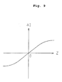
- Step S25 the total amount I1 and the total amount I2 of the light amounts, which are detected in Step S24, are compared with each other (Step S25), and the focus position of the projection optical system 15 is measured by using a result of the comparison performed in Step S25 (Step S26, measuring step).
- the intensity of the light transmitted through the recesses 40 of the phase pattern is identical with the intensity of the light transmitted through the protrusions 41 of the phase pattern as shown in a graph in Fig. 7 .
- the total amount I1 of the light amounts of the light received via the first light-receiving pattern 43a is equal to the total amount I2 of the light amounts of the light received via the second light-receiving pattern 44a.
- the adjustment of the focus position of the projection optical system 15 (adjusting step in Step S13), which is based on the result measured in Step S11 in the flow chart shown in Fig. 2 , is executed by calculating the adjustment amount for the focus position based on the measurement result so that the focus position of the projection optical system 15 is adjusted.
- the focus position is adjusted by using an optical member (for example, wedge-shaped pair glass members) constructing the projection optical system 15.
- an optical member for example, wedge-shaped pair glass members
- the light-receiving patterns 43a, 44a which are provided on the measuring device 20, are used to selectively extract the part of the phase pattern image (partial image) having the intensity corresponding to the area in which the phase of the phase pattern is relatively advanced, from the phase pattern image formed via the projection optical system 15 and the part of the phase pattern image (partial image) having the intensity corresponding to the area in which the phase of the phase pattern is relatively delayed, from the phase pattern image.
- the optical characteristic of the projection optical system 15 can be measured highly accurately based on the light amounts of the light in relation to the respective partial images extracted by the sensor section 20a.
- the optical characteristic of the projection optical system 15 can be adjusted by using the obtained measurement result; and it is possible to obtain the projection optical system 15 having the satisfactory optical characteristic. Therefore, the pattern image of the mask M can be formed at a high resolution on the wafer W via the projection optical system 15 having the satisfactory optical characteristic.
- the part of the phase pattern image (partial image) having the intensity corresponding to the area in which the phase of the phase pattern is relatively advanced is selectively extracted from the phase pattern image
- the part of the phase pattern image (partial image) having the intensity corresponding to the area in which the phase of the phase pattern is relatively delayed is selectively extracted from the phase pattern image to detect the light amounts of the light in relation to the respective extracted partial images. Therefore, although the recesses 40 and the protrusions 41 of the phase pattern having the high spatial resolution are used, it is possible to receive the light by the sensor such as CCD or the like having a rough spatial resolution. Therefore, the required measured value can be correctly detected; and it is possible to highly accurately measure the optical characteristic (focus position) of the projection optical system 15.
- the optical characteristic of the projection optical system 15 is measured, and the optical characteristic of the projection optical system 15 is adjusted by using the obtained measurement result. Therefore, it is possible to obtain the optical system having the satisfactory optical characteristic in which the aberration is sufficiently corrected.
- the optical characteristic of the projection optical system 15 is measured and adjusted in accordance with the method for measuring the optical characteristic and the method for adjusting the optical characteristic concerning this embodiment. Therefore, it is possible to produce the exposure apparatus provided with the projection optical system having the satisfactory optical characteristic in which the aberration is sufficiently corrected.
- the focus position of the projection optical system 15 is measured by using the phase pattern as shown in Fig. 4 and the light-receiving pattern as shown in Figs. 5 and 6 .
- a measuring mask which is formed with two or more phase patterns having identical shapes, is used.
- the focus position of the projection optical system 15 can be measured at a plurality of image heights in the projection area of the projection optical system 15.
- Fig. 10 shows a construction of a measuring mask M2 formed with five phase patterns.
- the measuring mask M2 is formed with phase pattern areas 50 to 54 for performing the measurement at five points having different image heights in the projection area of the projection optical system 15.
- Fig. 11 shows a construction of the phase pattern area 50.
- the phase pattern areas 51 to 54 are constructed in the same manner as the phase pattern area 50.
- two phase patterns which are of mutually different types, are formed in the phase pattern area 50.
- a first phase pattern 50a and a second phase pattern 50b which are perpendicular to each other, are formed as the two phase patterns of the different types.
- Each of the two phase patterns 50a, 50b is formed of a transmission type line-and-space pattern composed of recesses and protrusions each having a width of several hundreds nm.
- Fig. 12 shows a pattern plate 20A of the measuring device usable in a case that the optical characteristic of the projection optical system 15 is measured by using the measuring mask M2 shown in Fig. 10 .
- pattern areas 55 to 59 which correspond to the phase pattern areas 50 to 54, are formed on the upper surface of the pattern plate 20A.
- Fig. 13 shows a construction of the pattern area 55.
- the pattern areas 56 to 59 are constructed in the same manner as the pattern area 55.
- the pattern area 55 has a first light-receiving section or receiving portion 55a which receives the light transmitted through the phase pattern 50a via the projection optical system 15 and a second light-receiving section or receiving portion 55b which receives the light transmitted through the phase pattern 50b via the projection optical system 15.
- the first light-receiving section 55a has a first light-receiving pattern 60 and a second light-receiving pattern 61. Only the light, which is transmitted through the recesses of the phase pattern 50a, passes through the first light-receiving pattern 60, and only the light, which is transmitted through the protrusions of the phase pattern 50a, passes through the second light-receiving pattern 61.
- the second light-receiving section 55b has a first light-receiving pattern 62 and a second light-receiving pattern 63. Only the light, which is transmitted through the recesses of the phase pattern 50b, passes through the first light-receiving pattern 62, and only the light, which is transmitted through the protrusions of the phase pattern 50b, passes through the second light-receiving pattern 63.
- the measuring device 20 is connected to an unillustrated setting section which sets the light-receiving areas of the sensor section so that the lights, which pass through the first light-receiving pattern 60 or the second light-receiving pattern 61 of the first light-receiving section 55a and the first light-receiving pattern 62 or the second light-receiving pattern 63 of the second light-receiving section 55b respectively, are detected individually (independently).
- the lights each of which passes through one of the first light-receiving pattern 60 and the second light-receiving pattern 61 of the first light-receiving section 55a and the first light-receiving pattern 62 and the second light-receiving pattern 63 of the second light-receiving section 55b, can be detected distinctly respectively in accordance with the setting effected by the setting section.
- One or more reference aperture or reference apertures may be provided on the light-receiving pattern of the pattern plate 20A.
- the reference aperture may be provided on each of the light-receiving pattern areas 55 to 59.
- the image of the phase pattern can be simultaneously measured at a plurality of image heights in the projection area of the projection optical system 15. Therefore, it is possible to measure the optical characteristic of the projection optical system 15 quickly and highly accurately.
- the optical characteristic of the projection optical system 15, which includes the curvature of image or the field curvature, etc., can be measured by comparing the informations about the light in relation to the image of the phase pattern at the plurality of image heights described above.
- the optical characteristic of the projection optical system 15, which includes the curvature of image or the field curvature, etc., can be also measured by comparing obtained detection results at the respective image heights by detecting only the information about the light which passes through the first light-receiving pattern or the second light-receiving pattern at the plurality of image heights described above.
- the astigmatism of the projection optical system 15 can be measured by comparing the information about the light in relation to the images of the phase patterns perpendicular to each other in one pattern area.
- the spherical aberration of the projection optical system 15 it is appropriate to use a measuring mask provided with two or more phase patterns having mutually different pitches.
- the measurement is performed with different sensitivities and/or dynamic ranges of the measurement, it is also allowable to use two or more phase patterns having different directions of pattern formation and/or different pattern shapes (including, for example, pattern line widths, pattern pitches, etc.).
- the focus deviation of the projection optical system 15 is measured by comparing the total amount I1 of the light amounts of the light received via the first light-receiving pattern 43a and the total amount I2 of the light amounts of the light received via the second light-receiving pattern 44a.
- the light amount of the light received via the first light-receiving pattern 43a (or the second light-receiving pattern 44a) may be detected at every predetermined period of time, and the time-dependent focus deviation of the projection optical system 15 may be measured from the time-dependent change amount of the total amount I1 (I2) of the light amounts of the light received via the first light-receiving pattern 43a (or the second light-receiving pattern 44a).
- the optical characteristic of the projection optical system is measured by using the phase pattern in which the recesses and the protrusions are repeatedly formed.
- the optical characteristic of the projection optical system may be measured by using about two sets of phase patterns as shown in Fig. 14 .
- the light, which is transmitted through the recesses of the phase pattern is received via the first light-receiving pattern, and the light, which is transmitted through the protrusions of the phase pattern, is received via the second light-receiving pattern.
- the light-receiving areas which receive the light via or passing through the first light-receiving pattern 43a and the light via or passing through the second light-receiving pattern 44a, are set by the setting section in the light-receiving area of one sensor section.
- a plurality of sensor sections may be used, and the lights may be received by the sensor sections, respectively.
- the first light-receiving pattern for allowing the light transmitted through the recesses of the phase pattern to pass therethrough and the second light-receiving pattern for allowing the light transmitted through the protrusions of the phase pattern to pass therethrough are provided on one pattern plate.
- the first light-receiving pattern and the second light-receiving pattern may be provided distinctly on two pattern plates in a separated manner.
- the wedge-shaped pair glass members are rotated relative to each other, and/or the position of the stage is controlled.
- the optical characteristic of the projection optical system 15 may be adjusted by performing movement of at least one of the optical members constructing the projection optical system 15 in the optical axis direction of the projection optical system 15, shift or inclination of the at least one optical member in the direction perpendicular to the optical axis of the projection optical system 15, and/or rotation of the at least one optical member about the center of the optical axis of the projection optical system 15.
- the focus position of the projection optical system 15 is simultaneously measured at the plurality of image heights in the projection area of the projection optical system 15.
- the wafer stage may be driven and controlled so as to make the measuring device, which is provided with the light-receiving pattern, be successively subjected to the scanning to arrive at positions at which two or more images of the phase pattern of the different image heights are formed, such that the focus positions at the different image heights are successively detected.
- the optical characteristic of the projection optical system is measured by using the transmission type phase pattern and the transmission type light-receiving pattern.
- the optical characteristic of the projection optical system may be measured by using at least one of a reflection type phase pattern and a reflection type light-receiving pattern.
- This embodiment is illustrative of the exemplary case in which the light is extracted by transmitting the light through the light-receiving pattern.
- the light may be extracted such that the light is shielded by a light-receiving pattern, and the light is transmitted through or reflected by the surroundings of the light-receiving pattern.
- the light amount of the measuring light which passed through the reference aperture is monitored so that no influence is exerted by the change of the light amount of the illumination light.
- the embodiment has been explained, which uses the spatially different light-receiving patterns to extract the light transmitted through the recesses of the phase pattern and the light transmitted through the protrusions of the phase pattern.
- a liquid crystal display device may be used as the pattern plate to electrically generate the light-receiving pattern.
- a shutter mechanism may be provided for the pattern plate to mechanically prepare the light-receiving pattern.
- the exemplary case has been explained by way of example, in which the projection exposure apparatus is provided with the measuring device for measuring the optical characteristic of the projection optical system 15, and the optical characteristic of the projection optical system 15 is measured and adjusted after installing the projection optical system 15 in the projection exposure apparatus.
- the optical characteristic of the projection optical system 15 may be measured in accordance with the method for measuring the optical characteristic according to this embodiment and the optical characteristic may be adjusted before installing the projection optical system 15 in the projection exposure apparatus.
- the optical characteristic of the projection optical system 15 can be also adjusted by machining or processing (for example, repolishing) or exchanging at least one of the optical members constructing the projection optical system 15, in addition to the adjustment of the optical characteristic of the projection optical system 15 as described above.
- the optical characteristic of the projection optical system 15 is measured by radiating the measuring light from the object side of the projection optical system 15 and detecting the measuring light via the image plane of the projection optical system 15.
- the measuring light may be radiated from the image plane side of the projection optical system 15, and the measuring light may be detected via the object plane of the projection optical system 15. That is, the optical characteristic of the projection optical system 15 may be measured by arranging the phase pattern on the image plane side of the projection optical system 15 and arranging the light-receiving pattern on the object plane side of the projection optical system 15.
- the method for measuring the optical characteristic of the projection optical system is explained in this embodiment. However, it is possible to measure the optical characteristic of an optical system of any other optical apparatus, for example, a microscope, etc.
- the embodiment of the present invention is also applicable to a liquid immersion type exposure apparatus in which the liquid is intervened between the projection optical system and the wafer.
- the construction has been explained, in which the measuring device 20 is attached to the wafer stage 16.
- the measuring device 20 may be provided detachably with respect to the wafer stage 16. Further, both of the wafer stage and the measuring stage may be prepared for the exposure apparatus, and the measuring device 20 may be provided on the measuring stage.
- the embodiment of the present invention is also applicable to an EUV exposure apparatus which includes an illumination optical system, a projection optical system, etc. constructed of reflection type optical members, wherein the extreme ultraviolet light (EUV light) is used as the exposure light.
- EUV light extreme ultraviolet light
- a microdevice (a semiconductor element, an image pickup element, a liquid crystal display element, a thin film magnetic head, etc.) can be produced by exposing a photosensitive substrate (wafer W) with a transfer pattern formed by a mask M by using the projection optical system 15 (exposure step).
- a photosensitive substrate wafer W
- exposure step a transfer pattern formed by a mask M
- An explanation will be made below with reference to a flow chart shown in Fig. 15 about an exemplary procedure adopted upon obtaining the semiconductor device as the microdevice by forming a predetermined circuit pattern on the wafer W, etc. as the photosensitive substrate by using the projection exposure apparatus according to the embodiment described above.
- Step S301 shown in Fig. 15 a metal film is vapor-deposited on each of wafers W of 1 lot. Subsequently, in Step S302, a photoresist is coated on a surface of the metal film on each of the wafers W of 1 lot.
- Step S303 the pattern, which is formed on the mask M, is illuminated with the illumination light by using the projection exposure apparatus according to the embodiment described above (illuminating step). The image of the pattern illuminated with the illumination light is successively transferred to the respective shot areas on each of the wafers W of 1 lot to perform the exposure via the projection optical system 15 having the optical characteristic measured and adjusted in accordance with the optical characteristic measuring method and the optical characteristic adjusting method according to this embodiment (exposure step).
- Step S304 the photoresist on each of the wafers W of 1 lot is developed in Step S304, and then the etching is performed by using the resist pattern as a mask on each of the wafers W of 1 lot in Step S305. Accordingly, the circuit pattern, which corresponds to the pattern of the mask M, is formed on each of the shot areas on each of the wafers W.
- Step S301 to Step S305 the metal is vapor-deposited on the wafer W, and the surface of the metal film is coated with the resist to perform the respective steps of the exposure, the development, and the etching.
- a silicon oxide film may be formed on the wafer W prior to these steps, and then the surface of the silicon oxide film may be coated with the resist to perform the respective steps of the exposure, the development, the etching, etc.
- the present invention relates to the theme or the subject included in Japanese Patent Application No. 2007-168021 filed on June 26, 2007 , the entire disclosure of which is evidently incorporated herein by reference.
- the optical characteristic adjusting method of the present invention is useful to measure the optical characteristic of the optical system usable to produce the electronic device such as the semiconductor element, the liquid crystal display element or the like in the lithography step.
- the optical characteristic of the optical system can be adjusted highly accurately by using the exposure apparatus provided with the optical system adjusted in accordance with the optical characteristic adjusting method of the present invention and the exposure method using the exposure apparatus.
- the exposure apparatus which is provided with the optical system having the satisfactory optical characteristic, can be produced in accordance with the exposure apparatus producing method for producing the exposure apparatus.
Landscapes
- Physics & Mathematics (AREA)
- General Physics & Mathematics (AREA)
- Health & Medical Sciences (AREA)
- Engineering & Computer Science (AREA)
- Environmental & Geological Engineering (AREA)
- Epidemiology (AREA)
- Public Health (AREA)
- Geometry (AREA)
- Chemical & Material Sciences (AREA)
- Analytical Chemistry (AREA)
- Exposure And Positioning Against Photoresist Photosensitive Materials (AREA)
- Testing Of Optical Devices Or Fibers (AREA)
Applications Claiming Priority (2)
| Application Number | Priority Date | Filing Date | Title |
|---|---|---|---|
| JP2007168021 | 2007-06-26 | ||
| PCT/JP2008/061495 WO2009001834A1 (fr) | 2007-06-26 | 2008-06-24 | Procédé de mesure de caractéristique optique, procédé d'ajustement de caractéristique optique, dispositif d'exposition, procédé d'exposition, et procédé de fabrication de dispositif d'exposition |
Publications (1)
| Publication Number | Publication Date |
|---|---|
| EP2172965A1 true EP2172965A1 (fr) | 2010-04-07 |
Family
ID=40185648
Family Applications (1)
| Application Number | Title | Priority Date | Filing Date |
|---|---|---|---|
| EP08777560A Withdrawn EP2172965A1 (fr) | 2007-06-26 | 2008-06-24 | Procédé de mesure de caractéristique optique, procédé d'ajustement de caractéristique optique, dispositif d'exposition, procédé d'exposition, et procédé de fabrication de dispositif d'exposition |
Country Status (6)
| Country | Link |
|---|---|
| US (1) | US20100177290A1 (fr) |
| EP (1) | EP2172965A1 (fr) |
| JP (1) | JPWO2009001834A1 (fr) |
| KR (1) | KR20100049558A (fr) |
| TW (1) | TW200910020A (fr) |
| WO (1) | WO2009001834A1 (fr) |
Families Citing this family (1)
| Publication number | Priority date | Publication date | Assignee | Title |
|---|---|---|---|---|
| JP5785402B2 (ja) * | 2011-03-03 | 2015-09-30 | キヤノン株式会社 | 露光装置、デバイス製造方法および計測方法 |
Family Cites Families (6)
| Publication number | Priority date | Publication date | Assignee | Title |
|---|---|---|---|---|
| JPH08304999A (ja) * | 1995-05-11 | 1996-11-22 | Oki Electric Ind Co Ltd | 位相シフトマスク及びそれを用いた焦点位置検出方法 |
| JP3994209B2 (ja) * | 1998-08-28 | 2007-10-17 | 株式会社ニコン | 光学系の検査装置および検査方法並びに該検査装置を備えた位置合わせ装置および投影露光装置 |
| JP2000258300A (ja) * | 1999-03-11 | 2000-09-22 | Nikon Corp | 投影光学系の結像特性計測装置及び計測方法並びに露光装置 |
| JP3297423B2 (ja) * | 2000-08-09 | 2002-07-02 | 株式会社東芝 | フォーカステストマスク、並びにそれを用いたフォーカス及び収差の測定方法 |
| JP2002093690A (ja) * | 2000-09-19 | 2002-03-29 | Hitachi Ltd | 半導体装置の製造方法 |
| US20060103525A1 (en) * | 2004-11-03 | 2006-05-18 | Belle Enterprises, Inc. | Child safety sensor for a vehicle |
-
2008
- 2008-06-24 KR KR1020107001548A patent/KR20100049558A/ko not_active Ceased
- 2008-06-24 JP JP2009520603A patent/JPWO2009001834A1/ja active Pending
- 2008-06-24 EP EP08777560A patent/EP2172965A1/fr not_active Withdrawn
- 2008-06-24 WO PCT/JP2008/061495 patent/WO2009001834A1/fr not_active Ceased
- 2008-06-25 TW TW097123693A patent/TW200910020A/zh unknown
-
2009
- 2009-12-23 US US12/654,589 patent/US20100177290A1/en not_active Abandoned
Also Published As
| Publication number | Publication date |
|---|---|
| KR20100049558A (ko) | 2010-05-12 |
| TW200910020A (en) | 2009-03-01 |
| US20100177290A1 (en) | 2010-07-15 |
| WO2009001834A1 (fr) | 2008-12-31 |
| JPWO2009001834A1 (ja) | 2010-08-26 |
Similar Documents
| Publication | Publication Date | Title |
|---|---|---|
| KR102221714B1 (ko) | 리소그래피 공정에 의해 기판 상에 형성된 구조체를 측정하는 메트롤로지 장치, 리소그래피 시스템, 및 리소그래피 공정에 의해 기판 상에 형성된 구조체를 측정하는 방법 | |
| CN108398856B (zh) | 量测方法和设备、光刻系统和器件制造方法 | |
| TWI759779B (zh) | 度量衡方法及相關的度量衡及微影設備 | |
| US7656503B2 (en) | Exposure apparatus and image plane detecting method | |
| KR102160223B1 (ko) | 검사 시스템에서의 포커싱을 위한 디바이스 및 방법 | |
| JP4057847B2 (ja) | リソグラフィ投影装置の較正方法、パターニング装置、及びデバイス製造方法 | |
| WO2008038751A1 (fr) | Procédé de mesure de largeur de ligne, procédé de détection de statut de formation d'image, procédé d'ajustement, procédé d'exposition et procédé de fabrication de dispositif | |
| EP1150170A2 (fr) | Evaluation d'une caractéristique d'un système lithographique | |
| US6797443B2 (en) | Focus monitoring method, focus monitoring apparatus, and method of manufacturing semiconductor device | |
| JP2008085326A (ja) | 検査装置、像投影装置、および基板特性測定方法 | |
| JP4032501B2 (ja) | 投影光学系の結像特性計測方法及び投影露光装置 | |
| KR20080073232A (ko) | 측정 장치, 노광 장치 및 디바이스 제조 방법 | |
| JPWO2005004211A1 (ja) | フォーカステストマスク、フォーカス測定方法、及び露光装置 | |
| TWI409595B (zh) | 測量設備,具有此測量設備之投影曝光設備以及裝置製造方法 | |
| JP2005030963A (ja) | 位置検出方法 | |
| TWI405043B (zh) | 像差測量方法,曝光設備,及裝置製造方法 | |
| US7586626B2 (en) | Measurement method, exposure method, exposure apparatus, and device fabrication method | |
| JP2007180152A (ja) | 測定方法及び装置、露光装置、並びに、デバイス製造方法 | |
| JP2005294404A (ja) | 測定装置、測定方法及びそれを有する露光装置及び露光方法、それを利用したデバイス製造方法 | |
| JP4677183B2 (ja) | 位置検出装置、および露光装置 | |
| JP4724558B2 (ja) | 測定方法及び装置、露光装置 | |
| JP4174324B2 (ja) | 露光方法及び装置 | |
| US20100177290A1 (en) | Optical characteristic measuring method, optical characteristic adjusting method, exposure apparatus, exposing method, and exposure apparatus manufacturing method | |
| EP2172966B1 (fr) | Procédé de mesure de caractéristique optique, procédé d'ajustement de caractéristique optique, dispositif d'exposition, et procédé d'exposition | |
| JP2002015992A (ja) | リソグラフィ・プロセス及びリソグラフィ・システムの評価方法、基板処理装置の調整方法、リソグラフィ・システム、露光方法及び装置、並びに感光材料の状態の測定方法 |
Legal Events
| Date | Code | Title | Description |
|---|---|---|---|
| PUAI | Public reference made under article 153(3) epc to a published international application that has entered the european phase |
Free format text: ORIGINAL CODE: 0009012 |
|
| 17P | Request for examination filed |
Effective date: 20100126 |
|
| AK | Designated contracting states |
Kind code of ref document: A1 Designated state(s): AT BE BG CH CY CZ DE DK EE ES FI FR GB GR HR HU IE IS IT LI LT LU LV MC MT NL NO PL PT RO SE SI SK TR |
|
| AX | Request for extension of the european patent |
Extension state: AL BA MK RS |
|
| REG | Reference to a national code |
Ref country code: HK Ref legal event code: DE Ref document number: 1136691 Country of ref document: HK |
|
| RAP1 | Party data changed (applicant data changed or rights of an application transferred) |
Owner name: NIKON CORPORATION |
|
| DAX | Request for extension of the european patent (deleted) | ||
| RAP1 | Party data changed (applicant data changed or rights of an application transferred) |
Owner name: NIKON CORPORATION |
|
| STAA | Information on the status of an ep patent application or granted ep patent |
Free format text: STATUS: THE APPLICATION HAS BEEN WITHDRAWN |
|
| 18W | Application withdrawn |
Effective date: 20160222 |
|
| REG | Reference to a national code |
Ref country code: HK Ref legal event code: WD Ref document number: 1136691 Country of ref document: HK |