EP2173024A2 - Agencement de commutation doté d'un transformateur élévateur de tension et commutateur doté d'un tel agencement de commutation - Google Patents
Agencement de commutation doté d'un transformateur élévateur de tension et commutateur doté d'un tel agencement de commutation Download PDFInfo
- Publication number
- EP2173024A2 EP2173024A2 EP09012379A EP09012379A EP2173024A2 EP 2173024 A2 EP2173024 A2 EP 2173024A2 EP 09012379 A EP09012379 A EP 09012379A EP 09012379 A EP09012379 A EP 09012379A EP 2173024 A2 EP2173024 A2 EP 2173024A2
- Authority
- EP
- European Patent Office
- Prior art keywords
- circuit
- boost converter
- direct current
- voltage
- circuit arrangement
- Prior art date
- Legal status (The legal status is an assumption and is not a legal conclusion. Google has not performed a legal analysis and makes no representation as to the accuracy of the status listed.)
- Granted
Links
Images


Classifications
-
- H—ELECTRICITY
- H02—GENERATION; CONVERSION OR DISTRIBUTION OF ELECTRIC POWER
- H02M—APPARATUS FOR CONVERSION BETWEEN AC AND AC, BETWEEN AC AND DC, OR BETWEEN DC AND DC, AND FOR USE WITH MAINS OR SIMILAR POWER SUPPLY SYSTEMS; CONVERSION OF DC OR AC INPUT POWER INTO SURGE OUTPUT POWER; CONTROL OR REGULATION THEREOF
- H02M3/00—Conversion of DC power input into DC power output
- H02M3/02—Conversion of DC power input into DC power output without intermediate conversion into AC
- H02M3/04—Conversion of DC power input into DC power output without intermediate conversion into AC by static converters
- H02M3/10—Conversion of DC power input into DC power output without intermediate conversion into AC by static converters using discharge tubes with control electrode or semiconductor devices with control electrode
- H02M3/145—Conversion of DC power input into DC power output without intermediate conversion into AC by static converters using discharge tubes with control electrode or semiconductor devices with control electrode using devices of a triode or transistor type requiring continuous application of a control signal
- H02M3/155—Conversion of DC power input into DC power output without intermediate conversion into AC by static converters using discharge tubes with control electrode or semiconductor devices with control electrode using devices of a triode or transistor type requiring continuous application of a control signal using semiconductor devices only
-
- H—ELECTRICITY
- H02—GENERATION; CONVERSION OR DISTRIBUTION OF ELECTRIC POWER
- H02J—ELECTRIC POWER NETWORKS; CIRCUIT ARRANGEMENTS OR SYSTEMS FOR SUPPLYING OR DISTRIBUTING ELECTRIC POWER; SYSTEMS FOR STORING ELECTRIC ENERGY
- H02J3/00—Circuit arrangements for AC mains or AC distribution networks
- H02J3/38—Arrangements for feeding a single network from two or more generators or sources in parallel; Arrangements for feeding already energised networks from additional generators or sources in parallel
- H02J3/381—Dispersed generators
-
- H—ELECTRICITY
- H02—GENERATION; CONVERSION OR DISTRIBUTION OF ELECTRIC POWER
- H02J—ELECTRIC POWER NETWORKS; CIRCUIT ARRANGEMENTS OR SYSTEMS FOR SUPPLYING OR DISTRIBUTING ELECTRIC POWER; SYSTEMS FOR STORING ELECTRIC ENERGY
- H02J2101/00—Supply or distribution of decentralised, dispersed or local electric power generation
- H02J2101/20—Dispersed power generation using renewable energy sources
- H02J2101/22—Solar energy
- H02J2101/24—Photovoltaics
-
- H—ELECTRICITY
- H02—GENERATION; CONVERSION OR DISTRIBUTION OF ELECTRIC POWER
- H02M—APPARATUS FOR CONVERSION BETWEEN AC AND AC, BETWEEN AC AND DC, OR BETWEEN DC AND DC, AND FOR USE WITH MAINS OR SIMILAR POWER SUPPLY SYSTEMS; CONVERSION OF DC OR AC INPUT POWER INTO SURGE OUTPUT POWER; CONTROL OR REGULATION THEREOF
- H02M1/00—Details of apparatus for conversion
- H02M1/0067—Converter structures employing plural converter units, other than for parallel operation of the units on a single load
- H02M1/007—Plural converter units in cascade
-
- Y—GENERAL TAGGING OF NEW TECHNOLOGICAL DEVELOPMENTS; GENERAL TAGGING OF CROSS-SECTIONAL TECHNOLOGIES SPANNING OVER SEVERAL SECTIONS OF THE IPC; TECHNICAL SUBJECTS COVERED BY FORMER USPC CROSS-REFERENCE ART COLLECTIONS [XRACs] AND DIGESTS
- Y02—TECHNOLOGIES OR APPLICATIONS FOR MITIGATION OR ADAPTATION AGAINST CLIMATE CHANGE
- Y02E—REDUCTION OF GREENHOUSE GAS [GHG] EMISSIONS, RELATED TO ENERGY GENERATION, TRANSMISSION OR DISTRIBUTION
- Y02E10/00—Energy generation through renewable energy sources
- Y02E10/50—Photovoltaic [PV] energy
- Y02E10/56—Power conversion systems, e.g. maximum power point trackers
Definitions
- the present invention relates to a circuit arrangement with a step-up converter for increasing a DC voltage provided and an inverter circuit having such a circuit arrangement.
- the present invention particularly relates to a circuit arrangement with a step-up converter for increasing a DC voltage provided by a photovoltaic generator and a solar inverter circuit having such a circuit arrangement.
- An inverter usually requires an intermediate circuit voltage of a certain size to generate an alternating voltage. Optimum efficiency is achieved if this DC link voltage is adapted exactly to the AC voltage to be generated.
- photovoltaic generators usually deliver a strongly fluctuating DC voltage.
- an input voltage range of 1: 2 at full load or 1: 2.5 from full load to no load is desirable.
- boost converter which boosts the variable DC voltage to a relatively constant DC link voltage.
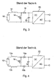
- FIG. 3 The structure of a conventional standard inverter circuit (step-up converter) is in FIG. 3 illustrated.
- a photovoltaic generator 10 provides a variable DC voltage. This is set high with the boost converter, which includes a throttle 12, a power switch 14 and a diode 16, to the intermediate circuit voltage, which is applied to an intermediate circuit capacitor 18. The downstream inverter 20 then converts the intermediate circuit voltage into an alternating voltage.
- the power switch 14 is periodically turned on and off.
- the clock ratio is selected via an analog or digital control so that adjusts the desired DC link voltage.
- the power switch 14 is closed, power flows from the photovoltaic generator 10 into the reactor 12 and is latched there. If the power switch 14 is then opened, the current flows from the photovoltaic generator 10 via the diode 16 into the DC link capacitor 18, whereby the energy previously stored in the throttle 12 is also delivered to the DC link capacitor 18.
- FIG. 4 shows a development of this standard inverter circuit, as for example from the DE 10 2004 037 446 A1 is known.
- inverter circuit is different from the standard circuit of FIG. 3 by the symmetrical arrangement of two chokes 12a and 12b and the additional diode 16b, which is necessary for reasons of symmetry.
- the operation of this inverter circuit is the same as that of the Stindard inverter circuit described above.
- the symmetrical division of the chokes 12a, 12b causes the photovoltaic generator 10 to be at a different voltage level from ground, which is desirable for certain solar module types.
- boost converter in an inverter circuit also leads to losses that reduce the overall efficiency of the inverter circuit.
- the modified circuit of FIG. 4 there are still losses of the second diode 16b added, whereby the overall efficiency is even lower.
- the use of a boost converter is always associated with additional weight, volume and cost.
- the invention has for its object to provide an improved circuit arrangement with a DC power source and a boost converter. Furthermore, an improved inverter circuit is to be provided with a boost converter.
- the circuit arrangement includes a DC power source for providing a DC voltage; a boost converter for boosting the DC voltage supplied from the DC power source; and a link capacitor connected between the outputs of the boost converter.
- the DC power source comprises a first DC power source and a second DC power source and the boost converter is provided as a common boost converter for boosting both the DC voltage provided by the first DC power source and the DC voltage provided by the second DC power source.
- a common boost converter for a first DC power source and a second DC power source is used.
- the energy that must be cached in the boost converter or the circulating reactive power is much smaller.
- the losses of the boost converter are significantly reduced, whereby the overall efficiency of the circuit increases. Further advantages are a reduced cooling capacity due to the better efficiency, a reduction of the load on the semiconductor components of the boost converter, lower requirements in the design of the individual components and a relatively small number of components required to achieve a high efficiency.
- the common boost converter of the circuit arrangement includes a series circuit of a first inductance (eg throttle) and a first rectifier element (eg freewheeling diode or active power switch), which is connected between an output of the first DC power source and one side of the DC link capacitor, and a Series connection of a second inductor and a second rectifier element, which is connected between an output of the second DC power source and another side of the DC link capacitor.
- a first inductance eg throttle
- a first rectifier element eg freewheeling diode or active power switch
- the common boost converter includes a common switching element which is connected between the first and the second DC power source.
- This common switching element is connected, for example, between the connection between the first inductance and the first rectifier element and the connection between the second inductance and the second rectifier element.
- this common switching element is preferably a power switch which can be clocked at a fixed or variable frequency.
- the first and the second DC power source are parallel or series-connected partial current sources of a DC power source.
- the first and second DC power sources different (partial) strings of a solar module or a photovoltaic generator.
- first and the second inductance of the common boost converter can optionally be coupled together or formed separately from each other.
- the above-described circuit arrangement of the invention can be advantageously used in an inverter circuit which, in addition to this circuit arrangement, has an inverter for converting the DC voltage provided by the intermediate circuit capacitor into an AC voltage.
- two or more boost converters connected in parallel or in series can be connected to the input terminals of the inverter or to the DC link capacitor.
- FIG. 2 shows the exemplary structure of an inverter circuit according to the present invention.
- FIG. 1 FIG. 2 shows the exemplary structure of an inverter circuit according to the present invention.
- FIGS. 1 and 2 described conventional circuitry.
- the inverter circuit of the invention is very similar to the conventional arrangement of FIG. 4 according to the DE 10.2004 037 446 A1 , However, it differs significantly from this prior art by a different connection of the photovoltaic generator to the boost converter. This also results in a significantly changed mode of operation and, as a result, improved properties.
- the photovoltaic generator constituting the DC power source according to the invention is divided into two (partial) strings 10a, 10b each providing a DC voltage.
- the first and second DC power sources 10a, 10b are preferably symmetrical, i. generate substantially the same DC voltage for best results.
- the voltage per string 10a, 10b at full load is typically in the range between about 50% and 100% of the intermediate circuit voltage. In this way, an input voltage range of about 1: 2 at full load is achieved.
- both DC power sources 10a, 10b are connected to a common boost converter 12-16, to which an intermediate circuit capacitor 18 and finally an inverter 20 are connected downstream.
- this common boost converter 12-16 includes a series circuit of a first choke 12a and a first diode 16a, which is connected between an output of the first DC source 10a and one side of the DC link capacitor 18 is connected, and a series circuit of a second choke 12b and a second diode 16b, which is connected between an output of the second DC power source 10b and another side of the DC link capacitor 18.
- the common boost converter 12-16 includes a common power switch 14 connected between the first and second DC power sources 10a, 10b so as to be connected between the first reactor 12a and the first diode 16a and the connection between the second reactor 12b and the second diode 16b is connected.
- the two DC power sources 10a, 10b are in series with the power switch 14 closed and in parallel with open switch 14 via the first and the second diode 16a, 16b.
- energy is released into the DC link capacitor 18 both when the circuit breaker is closed and when the circuit breaker 14 is open.
- the energy that must be stored in the chokes 12a, 12b of the boost converter 12-16, or the circulating in the boost converter reactive power is much smaller.
- the two chokes 12a, 12b must be designed only about half as large and the load on the circuit breaker 14 and other semiconductor devices is reduced.
- the losses in the boost converter are significantly reduced, the overall efficiency of the inverter circuit is greater and the required cooling capacity is lower.
- the circuit breaker 14 If the DC voltage of the two strings 10a, 10b is about 50% or about 100% of the desired intermediate circuit voltage, then a static series or parallel connection of the two DC sources 10a, 10b is sufficient to generate the intermediate circuit voltage. Therefore, there are no switching losses on the circuit breaker 14. If the DC voltages of the two strings 10a, 10b each in the range between about 50% and 100% of the DC link voltage, the circuit breaker 14 is operated clocked. The duty cycle is controlled via a controller (not shown, analog or digital, for example, a conventional PWM control circuit) so that the desired DC link voltage arises. The duty cycle can vary between 100% (ie static series connection of 10a and 10b) and 0% (ie static parallel connection of 10a and 10b).
- FIG. 2 To illustrate the improved operation of the circuit arrangement according to the invention over conventional circuit arrangements with boost converters shows FIG. 2 a comparison of the efficiencies of the boost converter against the DC voltages provided by the power sources.
- the overall efficiencies of boost converters 12-16 are for the conventional circuit of FIG. 3 (Curve ⁇ ) and the circuit arrangement of the invention (curve A).
- the overall efficiency of the modified conventional circuit of FIG. 4 is still slightly below that of FIG. 3 ,
- the boost converter 12-16 does not clock, eliminating the switching losses of the circuit breaker 14 in both cases. In the circuit arrangement according to the invention, this is also possible with a DC voltage of 350 volts by the static series connection of the two partial strings 10a, 10b.
- FIG. 2 clearly shows that the efficiency of the boost converter and thus the overall efficiency of the inverter circuit could be significantly improved by the circuit arrangement according to the invention with little component complexity.
- the dependence of the efficiency or the losses of the boost converter from the DC voltage, which is provided by the photovoltaic generator 10, is substantially lower.
- the boost converter circuit 12-16 can be easily adapted to this case, even if the improvement in efficiency decreases with increasing asymmetry.
- the two DC sources or (partial) strings 10a, 10b may optionally consist of parallel or series-connected DC sources.
- the inductors 12a, 12b may either be coupled together or formed separately.
- the diodes can be used as first and second rectifier elements 16a, 16b optionally also active circuit breakers.
- the boost converter 12-16 can also be composed of two or more parallel and optionally out of phase working branches (multi-phase operation). In this case, individual branches can be completely switched off at partial load in order to increase the partial load efficiency.
- Umschwingnetzwerke can be installed (resonant switching).
- the control of the circuit breaker 14 can be done either with fixed or variable frequency. If the DC voltage of the partial strings 10a, 10b is close to 50% or 100% of the intermediate circuit voltage, the clock frequency of the power switch 14 may be lowered, for example, in order to reduce the switching losses. At values of 50% and 100% of the desired intermediate circuit voltage, preferably no clocking of the boost converter takes place, but the two DC power sources 10a, 10b are operated statically in parallel or in series. In such a static operation can the semiconductors are bridged for further efficiency increase, for example, with a relay.
- boost converter 12-16 can be connected in parallel or in series at the input of the inverter 20.
- inverter 20 itself various topologies can be used. Suitable are, for example, half bridges (for single-phase feed) and three-phase bridges.
- first and second DC power supplies 10a, 10b may also be used for the first and second DC power supplies 10a, 10b.
- fuel cells, thermoelectric generators, electromagnetic generators, accumulators, supercapacitors and the like are also suitable as DC sources of the circuit arrangement according to the invention.
- the circuit arrangement according to the invention with DC sources 10a, 10b, step-up converter 12-16 and DC link capacitor 18 can not only be used in combination with the downstream inverter 20, as in FIG FIG. 1 shown.
- the circuit arrangement of the invention can be advantageously used, for example, also for the direct supply of DC consumers or for the supply of DC intermediate circuits in other devices such as Motorfrequenzumrichtem.
Landscapes
- Engineering & Computer Science (AREA)
- Power Engineering (AREA)
- Dc-Dc Converters (AREA)
- Inverter Devices (AREA)
Applications Claiming Priority (1)
| Application Number | Priority Date | Filing Date | Title |
|---|---|---|---|
| DE102008050402.5A DE102008050402B4 (de) | 2008-10-04 | 2008-10-04 | Schaltungsanordnung mit einem Hochsetzsteller und Wechselrichterschaltung mit einer solchen Schaltungsanordnung |
Publications (3)
| Publication Number | Publication Date |
|---|---|
| EP2173024A2 true EP2173024A2 (fr) | 2010-04-07 |
| EP2173024A3 EP2173024A3 (fr) | 2010-09-29 |
| EP2173024B1 EP2173024B1 (fr) | 2016-07-13 |
Family
ID=41632466
Family Applications (1)
| Application Number | Title | Priority Date | Filing Date |
|---|---|---|---|
| EP09012379.5A Active EP2173024B1 (fr) | 2008-10-04 | 2009-09-30 | Agencement de commutation doté d'un transformateur élévateur de tension et commutateur doté d'un tel agencement de commutation |
Country Status (2)
| Country | Link |
|---|---|
| EP (1) | EP2173024B1 (fr) |
| DE (2) | DE102008050402B4 (fr) |
Cited By (5)
| Publication number | Priority date | Publication date | Assignee | Title |
|---|---|---|---|---|
| WO2012006746A1 (fr) | 2010-07-15 | 2012-01-19 | Woodward Ids Switzerland Ag | Transformateur d'intensité bidirectionnel pour courant continu |
| US20130057989A1 (en) * | 2010-05-03 | 2013-03-07 | Sma Solar Technology Ag | Method for limiting the generator voltage of a photovoltaic installation in case of danger and photovoltaic installation |
| US9257892B2 (en) | 2010-09-20 | 2016-02-09 | Danmarks Tekniske Universitet | Method and device for current driven electric energy conversion |
| CN109830952A (zh) * | 2019-03-21 | 2019-05-31 | 深圳供电局有限公司 | 电源系统 |
| CN110165655A (zh) * | 2019-06-04 | 2019-08-23 | 上海电器科学研究所(集团)有限公司 | 一种直流电源并机切换装置 |
Families Citing this family (12)
| Publication number | Priority date | Publication date | Assignee | Title |
|---|---|---|---|---|
| CN101904073B (zh) | 2007-10-15 | 2014-01-08 | Ampt有限公司 | 高效太阳能电力系统 |
| US9466737B2 (en) | 2009-10-19 | 2016-10-11 | Ampt, Llc | Solar panel string converter topology |
| DE102010006124B4 (de) | 2010-01-29 | 2015-04-09 | Platinum Gmbh | Schaltungsanordnung mit einem Hochsetzsteller und Wechselrichterschaltung mit einer solchen Schaltungsanordnung |
| US9042145B2 (en) | 2010-01-29 | 2015-05-26 | Platinum Gmbh | Circuit configuration with a step-up converter, and inverter circuit having such a circuit configuration |
| DE102011011330B4 (de) * | 2010-11-05 | 2018-02-08 | Sew-Eurodrive Gmbh & Co Kg | Tiefsetzsteller |
| DE102011011329B4 (de) | 2010-11-05 | 2018-02-08 | Sew-Eurodrive Gmbh & Co Kg | Hochsetzsteller |
| DE102011018357B4 (de) | 2011-04-20 | 2023-12-14 | Sew-Eurodrive Gmbh & Co Kg | Gleichspannungswandler |
| US9397497B2 (en) | 2013-03-15 | 2016-07-19 | Ampt, Llc | High efficiency interleaved solar power supply system |
| DE102013005070B4 (de) | 2013-03-22 | 2015-03-26 | Platinum Gmbh | Hoch-Tiefsetzsteller |
| DE102013022311B3 (de) | 2013-03-22 | 2024-10-31 | Sew-Eurodrive Gmbh & Co Kg | Verfahren zum Betreiben eines Hochsetzstellers und Hochsetzsteller |
| DE102013005277B3 (de) * | 2013-03-26 | 2014-07-03 | Platinum Gmbh | Verfahren zum Umwandeln von Gleichspannung in Wechselspannung und Wechselrichterschaltung dafür |
| DE102013005808B4 (de) | 2013-04-04 | 2018-02-08 | Sew-Eurodrive Gmbh & Co Kg | Gleichspannungswandler |
Citations (2)
| Publication number | Priority date | Publication date | Assignee | Title |
|---|---|---|---|---|
| US3459957A (en) | 1967-07-19 | 1969-08-05 | Ite Imperial Corp | Voltage regulator circuit |
| DE102006014780A1 (de) | 2006-03-29 | 2007-10-18 | Schekulin, Ulrich | Gleichstromsteller und Wechselrichter-Schaltungsanordnung |
Family Cites Families (4)
| Publication number | Priority date | Publication date | Assignee | Title |
|---|---|---|---|---|
| EP0584621B1 (fr) * | 1992-08-28 | 1995-04-12 | Siemens Aktiengesellschaft | Convertisseur direct de courant continu avec circuit Diode/résistance/capacité d'amortissement |
| US6963497B1 (en) | 2001-09-04 | 2005-11-08 | Edward Herbert | Power converter with an inductor input and switched capacitor outputs |
| DE102004037446B4 (de) | 2004-08-02 | 2006-11-02 | Conergy Ag | Trafoloser Wechselrichter für solare Netzeinspeisung |
| DE102006012164B4 (de) * | 2005-12-23 | 2009-12-17 | Fraunhofer-Gesellschaft zur Förderung der angewandten Forschung e.V. | Schaltungsanordnung zur Erzeugung einer Wechselspannung oder eines Wechselstroms |
-
2008
- 2008-10-04 DE DE102008050402.5A patent/DE102008050402B4/de active Active
-
2009
- 2009-09-30 EP EP09012379.5A patent/EP2173024B1/fr active Active
- 2009-09-30 DE DE202009018846U patent/DE202009018846U1/de not_active Expired - Lifetime
Patent Citations (2)
| Publication number | Priority date | Publication date | Assignee | Title |
|---|---|---|---|---|
| US3459957A (en) | 1967-07-19 | 1969-08-05 | Ite Imperial Corp | Voltage regulator circuit |
| DE102006014780A1 (de) | 2006-03-29 | 2007-10-18 | Schekulin, Ulrich | Gleichstromsteller und Wechselrichter-Schaltungsanordnung |
Cited By (11)
| Publication number | Priority date | Publication date | Assignee | Title |
|---|---|---|---|---|
| US20130057989A1 (en) * | 2010-05-03 | 2013-03-07 | Sma Solar Technology Ag | Method for limiting the generator voltage of a photovoltaic installation in case of danger and photovoltaic installation |
| US8837098B2 (en) * | 2010-05-03 | 2014-09-16 | Sma Solar Technology Ag | Method for limiting the generator voltage of a photovoltaic installation in case of danger and photovoltaic installation |
| WO2012006746A1 (fr) | 2010-07-15 | 2012-01-19 | Woodward Ids Switzerland Ag | Transformateur d'intensité bidirectionnel pour courant continu |
| CN103119840A (zh) * | 2010-07-15 | 2013-05-22 | 伍德沃德Ids瑞士股份有限公司 | 双向dc调节器 |
| AU2010357546B2 (en) * | 2010-07-15 | 2015-08-06 | Kk Wind Solutions A/S | Bidirectional DC converter |
| CN103119840B (zh) * | 2010-07-15 | 2016-06-15 | 伍德沃德Ids瑞士股份有限公司 | 双向dc调节器 |
| US9431898B2 (en) | 2010-07-15 | 2016-08-30 | Woodward Ids Switzerland Ag | Bidirectional DC-to-DC converter |
| US9257892B2 (en) | 2010-09-20 | 2016-02-09 | Danmarks Tekniske Universitet | Method and device for current driven electric energy conversion |
| CN109830952A (zh) * | 2019-03-21 | 2019-05-31 | 深圳供电局有限公司 | 电源系统 |
| CN110165655A (zh) * | 2019-06-04 | 2019-08-23 | 上海电器科学研究所(集团)有限公司 | 一种直流电源并机切换装置 |
| CN110165655B (zh) * | 2019-06-04 | 2024-01-30 | 上海电器科学研究所(集团)有限公司 | 一种直流电源并机切换装置 |
Also Published As
| Publication number | Publication date |
|---|---|
| DE102008050402A1 (de) | 2010-04-08 |
| DE202009018846U1 (de) | 2013-11-25 |
| EP2173024B1 (fr) | 2016-07-13 |
| EP2173024A3 (fr) | 2010-09-29 |
| DE102008050402B4 (de) | 2025-03-20 |
Similar Documents
| Publication | Publication Date | Title |
|---|---|---|
| EP2173024B1 (fr) | Agencement de commutation doté d'un transformateur élévateur de tension et commutateur doté d'un tel agencement de commutation | |
| EP2355325B1 (fr) | Agencement de commutation doté d'un transformateur élévateur de tension et commutateur doté d'un tel agencement de commutation | |
| EP2451064B1 (fr) | Convertisseur élévateur | |
| EP2363947B1 (fr) | Onduleur doté d'un réseau de bord alimenté de plusieurs manières | |
| EP1851846B1 (fr) | Onduleur | |
| EP2451065B1 (fr) | Onduleur comporter un convertisseur abaisseur | |
| DE102013005070B4 (de) | Hoch-Tiefsetzsteller | |
| EP2187510A1 (fr) | Circuit de démarrage d'un convertisseur de courant | |
| EP1956703A1 (fr) | Dispositif destiné à l'alimentation électrique à partir d'une source de courant | |
| DE102012202867B4 (de) | Ladeschaltung für eine Energiespeichereinrichtung und Verfahren zum Laden einer Energiespeichereinrichtung | |
| AT504944B1 (de) | Wechselrichter | |
| EP2515425B1 (fr) | Convertisseur de tension continue | |
| EP1976103B1 (fr) | Convertisseur à commutation douce et procédé de son commande | |
| DE102010060687A1 (de) | Leistungselektronische Wandlerstufe | |
| WO2009156021A1 (fr) | Circuit transformateur de tension et onduleur | |
| DE102013007056A1 (de) | Gleichspannungswandler | |
| EP2856625B1 (fr) | Alimentation en tension pour un onduleur | |
| EP2774255B1 (fr) | Convertisseur de tension comportant un premier circuit parallèle | |
| EP3139481B1 (fr) | Procede destine au fonctionnement d'une installation photovoltaïque | |
| WO2013189668A2 (fr) | Alimentation en énergie solaire d'un réseau de distribution d'énergie solaire au moyen d'un onduleur solaire | |
| DE102013005808B4 (de) | Gleichspannungswandler | |
| DE102024201378A1 (de) | Stationäre Gleichspannungs-Ladeeinrichtung für elektrisch angetriebene Fahrzeuge, Verfahren zum Bereitstellen einer Gleichspannungs-Ladeeinrichtung für elektrisch angetriebene Fahrzeuge | |
| WO2014184254A1 (fr) | Circuit convertisseur | |
| DE102012223170A1 (de) | Wechselrichter und Verfahren zum Betrieb eines Wechselrichters | |
| DE102012100494A1 (de) | Leistungszirkulation in Interleavingwandlern |
Legal Events
| Date | Code | Title | Description |
|---|---|---|---|
| PUAI | Public reference made under article 153(3) epc to a published international application that has entered the european phase |
Free format text: ORIGINAL CODE: 0009012 |
|
| AK | Designated contracting states |
Kind code of ref document: A2 Designated state(s): AT BE BG CH CY CZ DE DK EE ES FI FR GB GR HR HU IE IS IT LI LT LU LV MC MK MT NL NO PL PT RO SE SI SK SM TR |
|
| AX | Request for extension of the european patent |
Extension state: AL BA RS |
|
| PUAL | Search report despatched |
Free format text: ORIGINAL CODE: 0009013 |
|
| AK | Designated contracting states |
Kind code of ref document: A3 Designated state(s): AT BE BG CH CY CZ DE DK EE ES FI FR GB GR HR HU IE IS IT LI LT LU LV MC MK MT NL NO PL PT RO SE SI SK SM TR |
|
| AX | Request for extension of the european patent |
Extension state: AL BA RS |
|
| RIC1 | Information provided on ipc code assigned before grant |
Ipc: H02M 7/48 20070101ALN20100824BHEP Ipc: H02M 3/155 20060101AFI20100210BHEP Ipc: H02J 1/10 20060101ALI20100824BHEP |
|
| 17P | Request for examination filed |
Effective date: 20101007 |
|
| RAP1 | Party data changed (applicant data changed or rights of an application transferred) |
Owner name: PLATINUM GMBH |
|
| 17Q | First examination report despatched |
Effective date: 20150619 |
|
| RIC1 | Information provided on ipc code assigned before grant |
Ipc: H02J 1/10 20060101ALI20151217BHEP Ipc: H02M 3/155 20060101AFI20151217BHEP Ipc: H02M 7/48 20070101ALN20151217BHEP |
|
| GRAP | Despatch of communication of intention to grant a patent |
Free format text: ORIGINAL CODE: EPIDOSNIGR1 |
|
| RIC1 | Information provided on ipc code assigned before grant |
Ipc: H02M 7/48 20070101ALN20151218BHEP Ipc: H02J 1/10 20060101ALI20151218BHEP Ipc: H02M 3/155 20060101AFI20151218BHEP |
|
| INTG | Intention to grant announced |
Effective date: 20160126 |
|
| GRAS | Grant fee paid |
Free format text: ORIGINAL CODE: EPIDOSNIGR3 |
|
| GRAA | (expected) grant |
Free format text: ORIGINAL CODE: 0009210 |
|
| AK | Designated contracting states |
Kind code of ref document: B1 Designated state(s): AT BE BG CH CY CZ DE DK EE ES FI FR GB GR HR HU IE IS IT LI LT LU LV MC MK MT NL NO PL PT RO SE SI SK SM TR |
|
| REG | Reference to a national code |
Ref country code: GB Ref legal event code: FG4D Free format text: NOT ENGLISH |
|
| REG | Reference to a national code |
Ref country code: AT Ref legal event code: REF Ref document number: 813007 Country of ref document: AT Kind code of ref document: T Effective date: 20160715 Ref country code: CH Ref legal event code: EP |
|
| REG | Reference to a national code |
Ref country code: IE Ref legal event code: FG4D Free format text: LANGUAGE OF EP DOCUMENT: GERMAN |
|
| REG | Reference to a national code |
Ref country code: DE Ref legal event code: R096 Ref document number: 502009012802 Country of ref document: DE |
|
| REG | Reference to a national code |
Ref country code: FR Ref legal event code: PLFP Year of fee payment: 8 |
|
| REG | Reference to a national code |
Ref country code: CH Ref legal event code: NV Representative=s name: HEPP WENGER RYFFEL AG, CH Ref country code: CH Ref legal event code: PUE Owner name: SEW-EURODRIVE GMBH AND CO. KG, DE Free format text: FORMER OWNER: PLATINUM GMBH, DE |
|
| RAP2 | Party data changed (patent owner data changed or rights of a patent transferred) |
Owner name: SEW-EURODRIVE GMBH & CO. KG |
|
| REG | Reference to a national code |
Ref country code: SE Ref legal event code: TRGR |
|
| REG | Reference to a national code |
Ref country code: LT Ref legal event code: MG4D |
|
| REG | Reference to a national code |
Ref country code: NL Ref legal event code: MP Effective date: 20160713 |
|
| PG25 | Lapsed in a contracting state [announced via postgrant information from national office to epo] |
Ref country code: NL Free format text: LAPSE BECAUSE OF FAILURE TO SUBMIT A TRANSLATION OF THE DESCRIPTION OR TO PAY THE FEE WITHIN THE PRESCRIBED TIME-LIMIT Effective date: 20160713 Ref country code: IS Free format text: LAPSE BECAUSE OF FAILURE TO SUBMIT A TRANSLATION OF THE DESCRIPTION OR TO PAY THE FEE WITHIN THE PRESCRIBED TIME-LIMIT Effective date: 20161113 Ref country code: HR Free format text: LAPSE BECAUSE OF FAILURE TO SUBMIT A TRANSLATION OF THE DESCRIPTION OR TO PAY THE FEE WITHIN THE PRESCRIBED TIME-LIMIT Effective date: 20160713 Ref country code: NO Free format text: LAPSE BECAUSE OF FAILURE TO SUBMIT A TRANSLATION OF THE DESCRIPTION OR TO PAY THE FEE WITHIN THE PRESCRIBED TIME-LIMIT Effective date: 20161013 Ref country code: LT Free format text: LAPSE BECAUSE OF FAILURE TO SUBMIT A TRANSLATION OF THE DESCRIPTION OR TO PAY THE FEE WITHIN THE PRESCRIBED TIME-LIMIT Effective date: 20160713 |
|
| REG | Reference to a national code |
Ref country code: GB Ref legal event code: 732E Free format text: REGISTERED BETWEEN 20170105 AND 20170111 |
|
| PG25 | Lapsed in a contracting state [announced via postgrant information from national office to epo] |
Ref country code: PL Free format text: LAPSE BECAUSE OF FAILURE TO SUBMIT A TRANSLATION OF THE DESCRIPTION OR TO PAY THE FEE WITHIN THE PRESCRIBED TIME-LIMIT Effective date: 20160713 Ref country code: BE Free format text: LAPSE BECAUSE OF NON-PAYMENT OF DUE FEES Effective date: 20160930 Ref country code: LV Free format text: LAPSE BECAUSE OF FAILURE TO SUBMIT A TRANSLATION OF THE DESCRIPTION OR TO PAY THE FEE WITHIN THE PRESCRIBED TIME-LIMIT Effective date: 20160713 Ref country code: PT Free format text: LAPSE BECAUSE OF FAILURE TO SUBMIT A TRANSLATION OF THE DESCRIPTION OR TO PAY THE FEE WITHIN THE PRESCRIBED TIME-LIMIT Effective date: 20161114 Ref country code: ES Free format text: LAPSE BECAUSE OF FAILURE TO SUBMIT A TRANSLATION OF THE DESCRIPTION OR TO PAY THE FEE WITHIN THE PRESCRIBED TIME-LIMIT Effective date: 20160713 Ref country code: GR Free format text: LAPSE BECAUSE OF FAILURE TO SUBMIT A TRANSLATION OF THE DESCRIPTION OR TO PAY THE FEE WITHIN THE PRESCRIBED TIME-LIMIT Effective date: 20161014 |
|
| REG | Reference to a national code |
Ref country code: DE Ref legal event code: R097 Ref document number: 502009012802 Country of ref document: DE |
|
| PG25 | Lapsed in a contracting state [announced via postgrant information from national office to epo] |
Ref country code: EE Free format text: LAPSE BECAUSE OF FAILURE TO SUBMIT A TRANSLATION OF THE DESCRIPTION OR TO PAY THE FEE WITHIN THE PRESCRIBED TIME-LIMIT Effective date: 20160713 Ref country code: MC Free format text: LAPSE BECAUSE OF FAILURE TO SUBMIT A TRANSLATION OF THE DESCRIPTION OR TO PAY THE FEE WITHIN THE PRESCRIBED TIME-LIMIT Effective date: 20160713 Ref country code: RO Free format text: LAPSE BECAUSE OF FAILURE TO SUBMIT A TRANSLATION OF THE DESCRIPTION OR TO PAY THE FEE WITHIN THE PRESCRIBED TIME-LIMIT Effective date: 20160713 |
|
| PLBE | No opposition filed within time limit |
Free format text: ORIGINAL CODE: 0009261 |
|
| STAA | Information on the status of an ep patent application or granted ep patent |
Free format text: STATUS: NO OPPOSITION FILED WITHIN TIME LIMIT |
|
| PG25 | Lapsed in a contracting state [announced via postgrant information from national office to epo] |
Ref country code: DK Free format text: LAPSE BECAUSE OF FAILURE TO SUBMIT A TRANSLATION OF THE DESCRIPTION OR TO PAY THE FEE WITHIN THE PRESCRIBED TIME-LIMIT Effective date: 20160713 Ref country code: SM Free format text: LAPSE BECAUSE OF FAILURE TO SUBMIT A TRANSLATION OF THE DESCRIPTION OR TO PAY THE FEE WITHIN THE PRESCRIBED TIME-LIMIT Effective date: 20160713 Ref country code: BG Free format text: LAPSE BECAUSE OF FAILURE TO SUBMIT A TRANSLATION OF THE DESCRIPTION OR TO PAY THE FEE WITHIN THE PRESCRIBED TIME-LIMIT Effective date: 20161013 Ref country code: SK Free format text: LAPSE BECAUSE OF FAILURE TO SUBMIT A TRANSLATION OF THE DESCRIPTION OR TO PAY THE FEE WITHIN THE PRESCRIBED TIME-LIMIT Effective date: 20160713 Ref country code: CZ Free format text: LAPSE BECAUSE OF FAILURE TO SUBMIT A TRANSLATION OF THE DESCRIPTION OR TO PAY THE FEE WITHIN THE PRESCRIBED TIME-LIMIT Effective date: 20160713 |
|
| 26N | No opposition filed |
Effective date: 20170418 |
|
| REG | Reference to a national code |
Ref country code: IE Ref legal event code: MM4A |
|
| PG25 | Lapsed in a contracting state [announced via postgrant information from national office to epo] |
Ref country code: IE Free format text: LAPSE BECAUSE OF NON-PAYMENT OF DUE FEES Effective date: 20160930 |
|
| REG | Reference to a national code |
Ref country code: FR Ref legal event code: PLFP Year of fee payment: 9 |
|
| PG25 | Lapsed in a contracting state [announced via postgrant information from national office to epo] |
Ref country code: LU Free format text: LAPSE BECAUSE OF NON-PAYMENT OF DUE FEES Effective date: 20160930 Ref country code: SI Free format text: LAPSE BECAUSE OF FAILURE TO SUBMIT A TRANSLATION OF THE DESCRIPTION OR TO PAY THE FEE WITHIN THE PRESCRIBED TIME-LIMIT Effective date: 20160713 |
|
| REG | Reference to a national code |
Ref country code: BE Ref legal event code: MM Effective date: 20160930 |
|
| PG25 | Lapsed in a contracting state [announced via postgrant information from national office to epo] |
Ref country code: CY Free format text: LAPSE BECAUSE OF FAILURE TO SUBMIT A TRANSLATION OF THE DESCRIPTION OR TO PAY THE FEE WITHIN THE PRESCRIBED TIME-LIMIT Effective date: 20160713 Ref country code: HU Free format text: LAPSE BECAUSE OF FAILURE TO SUBMIT A TRANSLATION OF THE DESCRIPTION OR TO PAY THE FEE WITHIN THE PRESCRIBED TIME-LIMIT; INVALID AB INITIO Effective date: 20090930 |
|
| PG25 | Lapsed in a contracting state [announced via postgrant information from national office to epo] |
Ref country code: MT Free format text: LAPSE BECAUSE OF FAILURE TO SUBMIT A TRANSLATION OF THE DESCRIPTION OR TO PAY THE FEE WITHIN THE PRESCRIBED TIME-LIMIT Effective date: 20160713 Ref country code: MK Free format text: LAPSE BECAUSE OF FAILURE TO SUBMIT A TRANSLATION OF THE DESCRIPTION OR TO PAY THE FEE WITHIN THE PRESCRIBED TIME-LIMIT Effective date: 20160713 Ref country code: TR Free format text: LAPSE BECAUSE OF FAILURE TO SUBMIT A TRANSLATION OF THE DESCRIPTION OR TO PAY THE FEE WITHIN THE PRESCRIBED TIME-LIMIT Effective date: 20160713 |
|
| REG | Reference to a national code |
Ref country code: FR Ref legal event code: PLFP Year of fee payment: 10 |
|
| REG | Reference to a national code |
Ref country code: AT Ref legal event code: PC Ref document number: 813007 Country of ref document: AT Kind code of ref document: T Owner name: SEW-EURODRIVE GMBH & CO. KG, DE Effective date: 20180730 |
|
| REG | Reference to a national code |
Ref country code: CH Ref legal event code: U11 Free format text: ST27 STATUS EVENT CODE: U-0-0-U10-U11 (AS PROVIDED BY THE NATIONAL OFFICE) Effective date: 20251001 |
|
| PGFP | Annual fee paid to national office [announced via postgrant information from national office to epo] |
Ref country code: FI Payment date: 20250912 Year of fee payment: 17 |
|
| PGFP | Annual fee paid to national office [announced via postgrant information from national office to epo] |
Ref country code: DE Payment date: 20250930 Year of fee payment: 17 |
|
| PGFP | Annual fee paid to national office [announced via postgrant information from national office to epo] |
Ref country code: IT Payment date: 20250825 Year of fee payment: 17 |
|
| PGFP | Annual fee paid to national office [announced via postgrant information from national office to epo] |
Ref country code: GB Payment date: 20250807 Year of fee payment: 17 |
|
| PGFP | Annual fee paid to national office [announced via postgrant information from national office to epo] |
Ref country code: FR Payment date: 20250808 Year of fee payment: 17 Ref country code: AT Payment date: 20250909 Year of fee payment: 17 |
|
| PGFP | Annual fee paid to national office [announced via postgrant information from national office to epo] |
Ref country code: SE Payment date: 20250812 Year of fee payment: 17 |
|
| PGFP | Annual fee paid to national office [announced via postgrant information from national office to epo] |
Ref country code: CH Payment date: 20251001 Year of fee payment: 17 |
|
| REG | Reference to a national code |
Ref country code: DE Ref legal event code: R084 Ref document number: 502009012802 Country of ref document: DE |