EP2174384B1 - Connecteur electrique ameliore - Google Patents
Connecteur electrique ameliore Download PDFInfo
- Publication number
- EP2174384B1 EP2174384B1 EP08774652.5A EP08774652A EP2174384B1 EP 2174384 B1 EP2174384 B1 EP 2174384B1 EP 08774652 A EP08774652 A EP 08774652A EP 2174384 B1 EP2174384 B1 EP 2174384B1
- Authority
- EP
- European Patent Office
- Prior art keywords
- glazing
- adhesive
- electrical
- connector
- connection
- Prior art date
- Legal status (The legal status is an assumption and is not a legal conclusion. Google has not performed a legal analysis and makes no representation as to the accuracy of the status listed.)
- Revoked
Links
Images
Classifications
-
- H—ELECTRICITY
- H05—ELECTRIC TECHNIQUES NOT OTHERWISE PROVIDED FOR
- H05B—ELECTRIC HEATING; ELECTRIC LIGHT SOURCES NOT OTHERWISE PROVIDED FOR; CIRCUIT ARRANGEMENTS FOR ELECTRIC LIGHT SOURCES, IN GENERAL
- H05B3/00—Ohmic-resistance heating
- H05B3/84—Heating arrangements specially adapted for transparent or reflecting areas, e.g. for demisting or de-icing windows, mirrors or vehicle windshields
-
- H—ELECTRICITY
- H01—ELECTRIC ELEMENTS
- H01R—ELECTRICALLY-CONDUCTIVE CONNECTIONS; STRUCTURAL ASSOCIATIONS OF A PLURALITY OF MUTUALLY-INSULATED ELECTRICAL CONNECTING ELEMENTS; COUPLING DEVICES; CURRENT COLLECTORS
- H01R12/00—Structural associations of a plurality of mutually-insulated electrical connecting elements, specially adapted for printed circuits, e.g. printed circuit boards [PCB], flat or ribbon cables, or like generally planar structures, e.g. terminal strips, terminal blocks; Coupling devices specially adapted for printed circuits, flat or ribbon cables, or like generally planar structures; Terminals specially adapted for contact with, or insertion into, printed circuits, flat or ribbon cables, or like generally planar structures
- H01R12/50—Fixed connections
- H01R12/59—Fixed connections for flexible printed circuits, flat or ribbon cables or like structures
- H01R12/62—Fixed connections for flexible printed circuits, flat or ribbon cables or like structures connecting to rigid printed circuits or like structures
-
- H—ELECTRICITY
- H01—ELECTRIC ELEMENTS
- H01R—ELECTRICALLY-CONDUCTIVE CONNECTIONS; STRUCTURAL ASSOCIATIONS OF A PLURALITY OF MUTUALLY-INSULATED ELECTRICAL CONNECTING ELEMENTS; COUPLING DEVICES; CURRENT COLLECTORS
- H01R43/00—Apparatus or processes specially adapted for manufacturing, assembling, maintaining, or repairing of line connectors or current collectors or for joining electric conductors
- H01R43/02—Apparatus or processes specially adapted for manufacturing, assembling, maintaining, or repairing of line connectors or current collectors or for joining electric conductors for soldered or welded connections
- H01R43/0235—Apparatus or processes specially adapted for manufacturing, assembling, maintaining, or repairing of line connectors or current collectors or for joining electric conductors for soldered or welded connections for applying solder
-
- H—ELECTRICITY
- H05—ELECTRIC TECHNIQUES NOT OTHERWISE PROVIDED FOR
- H05B—ELECTRIC HEATING; ELECTRIC LIGHT SOURCES NOT OTHERWISE PROVIDED FOR; CIRCUIT ARRANGEMENTS FOR ELECTRIC LIGHT SOURCES, IN GENERAL
- H05B2203/00—Aspects relating to Ohmic resistive heating covered by group H05B3/00
- H05B2203/016—Heaters using particular connecting means
Definitions
- the present invention relates to an improved electrical connector, and to a glazing comprising such a connector.
- EP 0 413 614 A describes a method of making electrical connections between electrode arrangements (3a, 3b) formed on first and second substrates (1, 2) which is particularly advantageous for making connections in liquid crystal displays.
- the first substrate (1) is placed over the second substrate (2) with the respective electrodes (3a, 3b) in registry and with a UV-light-curable adhesive (4) therebetween.
- the UV-light-curable adhesive carries first and second kinds of particles (5, 6) dispersed therein.
- the first and second substrates (1, 2) are pressed against each other and exposed to UV light in order to harden the adhesive (4).
- the first kind of particles (5) are electrically conductive particles and preferably are resiliently deformable and function to establish current paths between the electrodes of the first and second substrates, and the second kind of particles (6) are smaller than the first and function to prevent the first kind of particles from being destroyed by excessive deformation.
- EP 0 535 491 A relates to a process for producing electrically conductive connections between conductor tracks which are arranged on the surface of a rigid printed circuit board which is used as a carrier and conductor tracks which are arranged on the surface of a flexible film which is used as a carrier, the conductor tracks having soldering surfaces in the region of the connections to be produced, at least one of two opposite soldering surfaces being coated with solder plate or solder, and the opposite soldering surfaces being soldered to one another by the use of heat and, possibly, pressure.
- connection points conducting tracks
- connection points conducting tracks
- the electrical connector of EP '600 is constructed from two insulating layers which lie adjacent and parallel to one another and which form the connector body. At one end of the body there is a connection zone where a number of metallic contacts, for example blobs of solder, are located. Each contact is electrically connected to an individual metallic conducting track; the conducting tracks extend between the insulating layers to the other end of the connector body to a hub for connection to a vehicle's power supply.
- Both insulating layers are made of the same material, for example a pressure-resistant polyimide material such as KaptonTM, and have the same dimensions. However in the connection zone, one layer is provided with a number of apertures to accommodate the metallic contacts. Prior to connection to a glazing, each of the contacts protrudes from its aperture to enable their subsequent positioning on, and connection to, the connection points.
- a pressure-resistant polyimide material such as KaptonTM
- a heating tool is typically pressed against the connector on the opposite side to, and in the region of, the metallic contacts to melt them via the intermediate insulating layer to create an electrical connection with the connection points.
- the connector is held in position under an applied pressure, which compresses the melting metallic contacts but does not compress the layers of insulating material.
- Adhesive may be applied around a peripheral edge of the connection zone (either on the connector or on the glazing) to provide a protective seal around the electrical connection.
- the present invention provides in a first aspect a flexible electrical connector for connection to an electrical element on a substrate such as glazing in a vehicle comprising:
- Such a connector does not suffer from the problems associated with the prior art connector described in EP 1 439 600 A2 during and after its connection to a substrate, in that there is no extraneous flow of conductive material and so no short circuits are observed, and there are no observed instances of splashing of the conductive material. Furthermore, provision of a peripheral adhesive band around each of the conductive areas instead of use of further insulating material in this zone (as per the prior art connector of EP '600) means that the connector is relatively flexible, making it suitable for use with both flat and curved substrates, and an impermeable physical and electrical seal is provided around each conductive area.
- the electrical element may comprise one or more connection points; the connector may cooperatively comprise a suitable number of areas of conductive material to correspond with the number of connection points. For example, if the electrical element includes three connection points, the connector may include three areas of conductive material. As for nature of the electrical element, this may be any functional device that requires connection to another device via an electrical connector.
- the adhesive is provided as a layer around each of the areas of conductive material to maximise the amount of adhesion possible between the first connection portion of the connector and the substrate.
- the adhesive may be a compressible adhesive.
- use of only moderate pressure with a heating tool applied directly onto the first connection portion allows for good thermal conductivity through this portion to reliably melt the conductive material and create a secure electrical connection with the electrical element on the substrate.
- the adhesive bond to the substrate may be reinforced on application of moderate heat and pressure in this way.
- the adhesive may be provided with a removable protective layer, which protects the adhesive from contamination and damage prior to the connector being connected to a substrate.
- the adhesive has a thickness of 500 ⁇ m or less, further preferably 300 ⁇ m or less and most preferably 150 ⁇ m or less.
- each of the areas of conductive material has a thickness less than the thickness of the adhesive.
- each of the areas of conductive material preferably has a thickness of 200 ⁇ m or less, further preferably 150 ⁇ m or less and most preferably 100 ⁇ m or less.
- the conductive material is solder.
- solder There are numerous lead-free and lead-containing solders known in the art, including one or more of materials such as tin, lead, copper, zinc, silver, bismuth, indium and antimony, any of which may be used.
- the solder may be pre-fluxed with a reducing agent which is designed to help remove impurities (for example oxidised metal) from the connection points to improve the electrical connection.
- the flux may be of the "non-clean" type meaning that no cleaning of the solder contacts is required post-soldering.
- the connector body may be made from any suitable material such as polyimide, and the electrical pathways may be metallic tracks, such as copper tracks.
- the second connection portion may be a hub for enabling connection of the connector to another device.
- a glazing comprising:
- the glazing may be flat or it may be curved - in either case the connector is flexible enough to enable satisfactory connection of it to a surface of the glazing.
- the thickness of the adhesive is greater than the thickness of each of the areas of conductive material prior to connection of the connector to the glazing, application of heat and pressure to the first connection portion of the connector by the heating tool ensures that a substantially uniform thickness is achieved for the conductive material and the adhesive.
- the force required to peel the adhesive from the surface of the glazing is preferably at least 10 N, further preferably at least 20 N and most preferably at least 30 N.
- the glazing may be a monolith or it may be a laminate comprising two or more panes of glazing material joined together by one or more plies of interlayer material. If the glazing is a laminate, the electrical element may be provided either on the interior or the exterior of the laminate.
- the one or more panes of glazing material may be panes of glass, preferably soda-lime-silica glass, which may be clear or body-tinted, or they may be panes of a rigid plastics material such as polycarbonate. Typically the panes of glazing material may be used in a thickness between 1 and 10 mm, preferably between 1.5 and 6 mm.
- the one or more plies of interlayer material may be a flexible plastics material, which may be clear or body-tinted, such as polyvinyl butyral, typically used in thicknesses of 0.76 mm or 0.38 mm.
- a glazing according to the invention is used as a vehicle glazing, which may be fitted into any window opening in the bodywork of a vehicle, such as a windscreen or a rear window glazing.
- the electrical element may be a functional device such as a busbar, an antenna, or the like.
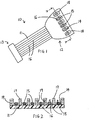
- Figure 1 shows electrical connector 10 which comprises connector body 11, at one end of which there is first connection portion 12 and at the other end there is second connection portion 13.
- First connection portion 12 is the portion which is capable of being connected (electrically and adhesively) to a substrate (not shown).
- Second connection portion 13 is in the form of a hub which is capable of being connected to an external device (not shown).
- First connection portion 12 comprises functional surface 14 on which is provided six areas of conductive material, each in the form of a patch of pre-fluxed solder 15. Each solder patch 15 is electrically connected to an individual electrical pathway, in the form of a copper track 16, of which there are six - one for each patch of solder 15. Each copper track 16 extends from first connection portion 12 inside connector body 11 (where they are electrically insulated) to second connection portion 13.
- first connection portion 12 (top" with reference to the orientation shown in the figures) is covered with removable protective layer, in the form of backing paper 17, to protect underlying adhesive layer 19.
- Both backing paper 17 and underlying adhesive layer 19 are provided with six apertures 18 in register with one another (backing paper 17 being in situ when apertures 18 were stamped into adhesive layer 19).
- Adhesive layer 19 is provided on functional surface 14 such that a peripheral band is formed around each patch of solder 15.
- Connector body 11 may be provided as a polyimide material, such as KaptonTM which is available from Du Pont (www.dupont.com).
- Adhesive layer 19 and corresponding protective backing paper 17 may be obtained from 3M (www.3m.com) as compressible adhesive 3MTM VHBTM Adhesive Transfer Tape F-9460PC, F-9469PC or F-9473PC.
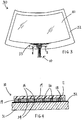
- Adhesive layer 19 is typically around 130 ⁇ m in thickness, compared to the smaller thickness of 80-90 ⁇ m for each solder patch 15. The difference in thickness is illustrated in Figure 2 - it ensures that when connector 10 is attached to a substrate, adhesive layer 19 contacts and adheres to the substrate before solder patches 15 are able to flow.
- FIGS 3 and 4 show glazing 30 to a surface of which an electrical connector 10 may be electrically and adhesively connected.
- Glazing 30 is in the form of a vehicle windscreen and it comprises a pane of glazing material, in the form of a pane of glass 31.
- an obscuration band 32 Around the periphery of glass pane 31 there is an obscuration band 32, which is there to disguise and protect the sealant (not shown) that is used to fix glazing 30 into a vehicle (not shown).
- Obscuration band 32 is made from opaque ink that has been screen printed onto the glazing and subsequently fired. However, it may be composed of and applied using any other known means, or it need not be there at all.
- connection point 34 of which there are six.
- Electrical connector 10 is attached to glazing 10 such that each of the six patches of solder 15 lies in register with one of the six connection points 34, with adhesive layer 19 forming physical and electrical barriers in between.
- Figure 4 shows adhesive layer 19 in contact with the obscuration band 32 on the surface of glazing 30 such that six sealed spaces are created with apertures 18.
- solder patches 15 have flowed without creation of short circuits or unsightly splashing of the solder.
- the thickness of adhesive layer 19 is reduced as compared to its thickness prior to attachment, as are the thicknesses of each solder patch 15, which are also reduced to around 60 ⁇ m.
- the strength of the adhesive bond created between adhesive layer 19 and obscuration band 32 on the surface of glazing 30 is such that the force required to peel connector away from the glazing is around 30 N, thereby providing protection for the electrical connections.
Landscapes
- Engineering & Computer Science (AREA)
- Manufacturing & Machinery (AREA)
- Connections Effected By Soldering, Adhesion, Or Permanent Deformation (AREA)
Claims (10)
- Connecteur électrique flexible (10) pour connexion à un élément électrique sur un substrat tel qu'un vitrage dans un véhicule comprenant :un corps de connecteur (11) présentant des première (12) et seconde (13) portions de connexion et deux ou plusieurs trajectoires électriques (16) fournies dans le corps de connecteur (11) et s'étendant entre les première (12) et seconde (13) portions de connexion,la première portion de connexion (12) ayant une surface fonctionnelle (14) pour se connecter au substrat et sur laquelle au moins deux surfaces exposées de matériau conducteur (15) sont fournies, dont chacune est en contact avec une trajectoire électrique correspondante (16), pour une connexion à l'élément électrique sur le substrat,dans lequel un adhésif (19) est fourni sur la surface fonctionnelle (14) de sorte que, à un minimum, une bande périphérique d'adhésif est formée autour de chacune des surfaces de matériau conducteur (15) pour une adhérence au substrat, etdans lequel le matériau conducteur (15) est un brasage,caractérisé en ce que chacune des surfaces de matériau conducteur (15) sur la première portion de connexion présente une épaisseur qui est inférieure à l'épaisseur de l'adhésif (19).
- Connecteur électrique (10) selon la revendication 1, dans lequel l'adhésif (19) est fourni comme une couche autour de chacune des surfaces de matériau conducteur (15).
- Connecteur électrique (10) selon la revendication 1 ou la revendication 2, dans lequel l'adhésif (19) est un adhésif compressible.
- Connecteur électrique (10) selon l'une quelconque des revendications précédentes, dans lequel l'adhésif (19) est muni d'une couche protectrice détachable (17).
- Connecteur électrique (10) selon l'une quelconque des revendications précédentes, dans lequel l'adhésif (19) présente une épaisseur de 500 µm ou inférieure.
- Connecteur électrique (10) selon l'une quelconque des revendications précédentes, dans lequel chacune des surfaces de matériau conducteur (15) présente une épaisseur de 200 µm ou inférieure.
- Connecteur électrique (10) selon l'une quelconque des revendications précédentes, dans lequel le brasage est pré-fluxé.
- Vitrage (30) comprenant :au moins un panneau de matériau de vitrage (31) muni d'un élément électrique (33), etun connecteur électrique (10) selon l'une quelconque des revendications précédentes électriquement connecté à l'élément électrique (33) et collé à une surface du vitrage.
- Vitrage (30) selon la revendication 8, dans lequel la force nécessaire pour détacher l'adhésif (19) de la surface du vitrage (30) est d'au moins 10 N.
- Utilisation d'un vitrage (30) selon la revendication 8 comme un vitrage de véhicule.
Applications Claiming Priority (2)
| Application Number | Priority Date | Filing Date | Title |
|---|---|---|---|
| GBGB0714723.4A GB0714723D0 (en) | 2007-07-30 | 2007-07-30 | Improved electrical connector |
| PCT/EP2008/058518 WO2009015975A1 (fr) | 2007-07-30 | 2008-07-02 | Connecteur électrique amélioré |
Publications (2)
| Publication Number | Publication Date |
|---|---|
| EP2174384A1 EP2174384A1 (fr) | 2010-04-14 |
| EP2174384B1 true EP2174384B1 (fr) | 2018-04-25 |
Family
ID=38528952
Family Applications (1)
| Application Number | Title | Priority Date | Filing Date |
|---|---|---|---|
| EP08774652.5A Revoked EP2174384B1 (fr) | 2007-07-30 | 2008-07-02 | Connecteur electrique ameliore |
Country Status (4)
| Country | Link |
|---|---|
| US (1) | US8373067B2 (fr) |
| EP (1) | EP2174384B1 (fr) |
| GB (1) | GB0714723D0 (fr) |
| WO (1) | WO2009015975A1 (fr) |
Families Citing this family (15)
| Publication number | Priority date | Publication date | Assignee | Title |
|---|---|---|---|---|
| CN103636060B (zh) | 2011-04-06 | 2016-03-23 | 法国圣戈班玻璃厂 | 用于天线结构的扁平导体连接元件 |
| CN104662471A (zh) * | 2012-06-05 | 2015-05-27 | Sage电致变色显示有限公司 | 电气馈通间隔件和连通性 |
| US9966673B2 (en) | 2013-08-16 | 2018-05-08 | Agc Automotive Americas R&D, Inc. | Window assembly with electrically conductive compressible member |
| PL3235339T3 (pl) | 2014-12-16 | 2019-08-30 | Saint-Gobain Glass France | Elektrycznie podgrzewana szyba antenowa jak również sposób jej wytwarzania |
| ES2849948T3 (es) | 2015-04-08 | 2021-08-24 | Saint Gobain | Luna con antena para vehículos |
| CN106463812A (zh) | 2015-04-08 | 2017-02-22 | 法国圣戈班玻璃厂 | 天线玻璃板 |
| JP6187918B2 (ja) * | 2015-04-23 | 2017-08-30 | パナソニックIpマネジメント株式会社 | 回路部材の接続構造、接続方法および接続材料 |
| US10843644B2 (en) * | 2016-09-16 | 2020-11-24 | Magna Mirrors Of America, Inc. | Vehicle liftgate window assembly with heater grid |
| GB201719522D0 (en) * | 2017-11-24 | 2018-01-10 | Pilkington Group Ltd | Electrical connector glazing havingthe same and method of fitting the glazing |
| WO2020075810A1 (fr) * | 2018-10-11 | 2020-04-16 | 積水ポリマテック株式会社 | Feuille de connexion électrique, et structure de feuille de verre avec extrémité |
| CN111856830A (zh) * | 2019-09-29 | 2020-10-30 | 法国圣戈班玻璃公司 | 具有分区段调控功能的玻璃以及玻璃分区段调控系统 |
| JP7756660B2 (ja) * | 2020-05-29 | 2025-10-20 | エージーシー グラス ユーロップ | 合わせガラスではんだ付けするためのフラットコネクタ |
| US12193122B2 (en) | 2021-03-11 | 2025-01-07 | Magna Mirrors Of America, Inc. | Vehicular window assembly with solderless electrical connection to heater grid |
| CN113385884B (zh) * | 2021-05-28 | 2022-06-10 | 浙江天能电池(江苏)有限公司 | 直连结构蓄电池汇流排修复方法 |
| US12424807B2 (en) | 2022-07-08 | 2025-09-23 | Agc Automotive Americas Co. | Method of manufacturing a window assembly with a solderless electrical connector |
Citations (11)
| Publication number | Priority date | Publication date | Assignee | Title |
|---|---|---|---|---|
| US4735847A (en) | 1983-12-27 | 1988-04-05 | Sony Corporation | Electrically conductive adhesive sheet, circuit board and electrical connection structure using the same |
| EP0413614A2 (fr) | 1989-08-18 | 1991-02-20 | Semiconductor Energy Laboratory Co., Ltd. | Connexions électriques et leur procédé de fabrication |
| EP0535491A1 (fr) | 1991-10-04 | 1993-04-07 | Bodenseewerk Gerätetechnik GmbH | Procédé de fabrication de connexions électriques conductrices sur des cartes de circuits imprimés |
| JPH0832195A (ja) | 1994-07-11 | 1996-02-02 | Nippondenso Co Ltd | 複合プリント基板の接続構造 |
| US5920125A (en) * | 1992-11-12 | 1999-07-06 | International Business Machines Corporation | Interconnection of a carrier substrate and a semiconductor device |
| US20010029119A1 (en) | 2000-04-04 | 2001-10-11 | Chung Kevin Kwong-Tai | Fine-pitch flexible electrical connector, and method for making same |
| US20020014703A1 (en) | 1997-07-21 | 2002-02-07 | Capote Miguel A. | Semiconductor flip-chip package and method for the fabrication thereof |
| US6495916B1 (en) | 1999-04-06 | 2002-12-17 | Oki Electric Industry Co., Ltd. | Resin-encapsulated semiconductor device |
| DE10301352B3 (de) | 2003-01-16 | 2004-07-15 | Saint-Gobain Sekurit Deutschland Gmbh & Co. Kg | Lötanschlusselement sowie Verfahren zum Herstellen eines Lötanschlusses |
| US20040231878A1 (en) | 2003-05-19 | 2004-11-25 | Takaaki Higashida | Electronic circuit connecting structure, and its connecting method |
| WO2006096631A1 (fr) | 2005-03-07 | 2006-09-14 | 3M Innovative Properties Company | Procede permettant de raccorder une carte de circuits imprimes souple a une autre carte de circuits imprimes |
Family Cites Families (8)
| Publication number | Priority date | Publication date | Assignee | Title |
|---|---|---|---|---|
| JPS5656174U (fr) * | 1979-10-04 | 1981-05-15 | ||
| US4433223A (en) * | 1981-08-24 | 1984-02-21 | Oak Industries Inc. | Pressure-sensitive adhesive and application thereof |
| US4589584A (en) * | 1985-01-31 | 1986-05-20 | International Business Machines Corporation | Electrical connection for polymeric conductive material |
| JPH01206575A (ja) * | 1988-02-15 | 1989-08-18 | Shin Etsu Polymer Co Ltd | 接着性熱融着形コネクタ |
| DE19856663C2 (de) * | 1998-12-09 | 2003-04-03 | Saint Gobain Sekurit D Gmbh | Kontaktvorrichtung für ein an einer Fensterscheibe angeordnetes elektrisches Funktionselement |
| US6288905B1 (en) | 1999-04-15 | 2001-09-11 | Amerasia International Technology Inc. | Contact module, as for a smart card, and method for making same |
| US6717819B1 (en) | 1999-06-01 | 2004-04-06 | Amerasia International Technology, Inc. | Solderable flexible adhesive interposer as for an electronic package, and method for making same |
| CN101253825A (zh) * | 2005-09-30 | 2008-08-27 | 松下电器产业株式会社 | 片状复合电子部件及其制造方法 |
-
2007
- 2007-07-30 GB GBGB0714723.4A patent/GB0714723D0/en not_active Ceased
-
2008
- 2008-07-02 WO PCT/EP2008/058518 patent/WO2009015975A1/fr not_active Ceased
- 2008-07-02 US US12/670,614 patent/US8373067B2/en active Active
- 2008-07-02 EP EP08774652.5A patent/EP2174384B1/fr not_active Revoked
Patent Citations (12)
| Publication number | Priority date | Publication date | Assignee | Title |
|---|---|---|---|---|
| US4735847A (en) | 1983-12-27 | 1988-04-05 | Sony Corporation | Electrically conductive adhesive sheet, circuit board and electrical connection structure using the same |
| EP0413614A2 (fr) | 1989-08-18 | 1991-02-20 | Semiconductor Energy Laboratory Co., Ltd. | Connexions électriques et leur procédé de fabrication |
| EP0535491A1 (fr) | 1991-10-04 | 1993-04-07 | Bodenseewerk Gerätetechnik GmbH | Procédé de fabrication de connexions électriques conductrices sur des cartes de circuits imprimés |
| US5920125A (en) * | 1992-11-12 | 1999-07-06 | International Business Machines Corporation | Interconnection of a carrier substrate and a semiconductor device |
| JPH0832195A (ja) | 1994-07-11 | 1996-02-02 | Nippondenso Co Ltd | 複合プリント基板の接続構造 |
| US20020014703A1 (en) | 1997-07-21 | 2002-02-07 | Capote Miguel A. | Semiconductor flip-chip package and method for the fabrication thereof |
| US6495916B1 (en) | 1999-04-06 | 2002-12-17 | Oki Electric Industry Co., Ltd. | Resin-encapsulated semiconductor device |
| US20010029119A1 (en) | 2000-04-04 | 2001-10-11 | Chung Kevin Kwong-Tai | Fine-pitch flexible electrical connector, and method for making same |
| DE10301352B3 (de) | 2003-01-16 | 2004-07-15 | Saint-Gobain Sekurit Deutschland Gmbh & Co. Kg | Lötanschlusselement sowie Verfahren zum Herstellen eines Lötanschlusses |
| EP1439600B1 (fr) | 2003-01-16 | 2018-05-09 | Saint-Gobain Glass France | Elément de raccordement par soudage |
| US20040231878A1 (en) | 2003-05-19 | 2004-11-25 | Takaaki Higashida | Electronic circuit connecting structure, and its connecting method |
| WO2006096631A1 (fr) | 2005-03-07 | 2006-09-14 | 3M Innovative Properties Company | Procede permettant de raccorder une carte de circuits imprimes souple a une autre carte de circuits imprimes |
Also Published As
| Publication number | Publication date |
|---|---|
| WO2009015975A1 (fr) | 2009-02-05 |
| US20100193242A1 (en) | 2010-08-05 |
| EP2174384A1 (fr) | 2010-04-14 |
| US8373067B2 (en) | 2013-02-12 |
| GB0714723D0 (en) | 2007-09-12 |
Similar Documents
| Publication | Publication Date | Title |
|---|---|---|
| EP2174384B1 (fr) | Connecteur electrique ameliore | |
| US9550457B2 (en) | Electro-optic device with ultrasonic solder bus | |
| JP6939985B2 (ja) | 調光ユニット | |
| US5748155A (en) | On-glass antenna and connector arrangement | |
| EP0307231B1 (fr) | Dispositif d'affichage | |
| JP2007504005A (ja) | 半田付け方法および半田組成物 | |
| KR20150036256A (ko) | 전기 접촉 수단을 갖는 복합 판유리 | |
| JPS63271867A (ja) | 電気導線付母線組立体 | |
| JP7119305B2 (ja) | 調光体 | |
| US7520416B2 (en) | Transparent window with non-transparent contact surface for a soldering bonding | |
| CN113498566A (zh) | 扁形导体连接元件 | |
| WO2023190256A1 (fr) | Pare-brise de véhicule | |
| CN106183729A (zh) | 窗用层叠板和窗用层叠板的制造方法 | |
| EP3644689A1 (fr) | Connecteur flexible | |
| JP6538836B2 (ja) | 導電性コーティング及びその上にはんだ付けされる金属条片を有するガラス板の製造方法、並びに、対応するガラス板 | |
| KR20210005272A (ko) | 전기적 연결 요소 및 연결 케이블이 있는 판유리 | |
| JP7376845B2 (ja) | 車両用窓ガラス | |
| CN107995775B (zh) | 自带过流保护柔性电路及制造工艺 | |
| CN116194280B (zh) | 具有复合玻璃板和扁平带状电缆的接线组件 | |
| KR20240057448A (ko) | 파손 감지용 리본 케이블, 적층 판유리와 연결 조립체, 파손 감지 방법 및 리본 케이블의 용도 | |
| KR101128568B1 (ko) | 태양전지 모듈 및 그 제조 방법, 그리고 상기 태양전지 모듈을 구비하는 모바일 장치 및 그 제조 방법 | |
| JPH02127620A (ja) | 電気光学装置及びその接続方法 | |
| JP7784056B2 (ja) | 金属端子付き車両用窓ガラス | |
| US20230276542A1 (en) | Glass product, method of applying connector to glazing, and connector | |
| JP2024030258A (ja) | 車両用窓ガラス、及び車両用窓ガラスの製造方法 |
Legal Events
| Date | Code | Title | Description |
|---|---|---|---|
| PUAI | Public reference made under article 153(3) epc to a published international application that has entered the european phase |
Free format text: ORIGINAL CODE: 0009012 |
|
| 17P | Request for examination filed |
Effective date: 20100113 |
|
| AK | Designated contracting states |
Kind code of ref document: A1 Designated state(s): AT BE BG CH CY CZ DE DK EE ES FI FR GB GR HR HU IE IS IT LI LT LU LV MC MT NL NO PL PT RO SE SI SK TR |
|
| AX | Request for extension of the european patent |
Extension state: AL BA MK RS |
|
| RIN1 | Information on inventor provided before grant (corrected) |
Inventor name: PAULUS, PETER Inventor name: BUESCHER, MICHAEL Inventor name: DERDA, MARTIN |
|
| DAX | Request for extension of the european patent (deleted) | ||
| 17Q | First examination report despatched |
Effective date: 20120522 |
|
| STAA | Information on the status of an ep patent application or granted ep patent |
Free format text: STATUS: EXAMINATION IS IN PROGRESS |
|
| REG | Reference to a national code |
Ref country code: DE Ref legal event code: R079 Ref document number: 602008055006 Country of ref document: DE Free format text: PREVIOUS MAIN CLASS: H01R0012080000 Ipc: H01R0012620000 |
|
| RIC1 | Information provided on ipc code assigned before grant |
Ipc: H05B 3/84 20060101ALI20170803BHEP Ipc: H01R 12/62 20110101AFI20170803BHEP Ipc: H01R 43/02 20060101ALI20170803BHEP |
|
| GRAP | Despatch of communication of intention to grant a patent |
Free format text: ORIGINAL CODE: EPIDOSNIGR1 |
|
| STAA | Information on the status of an ep patent application or granted ep patent |
Free format text: STATUS: GRANT OF PATENT IS INTENDED |
|
| INTG | Intention to grant announced |
Effective date: 20170912 |
|
| GRAS | Grant fee paid |
Free format text: ORIGINAL CODE: EPIDOSNIGR3 |
|
| GRAA | (expected) grant |
Free format text: ORIGINAL CODE: 0009210 |
|
| STAA | Information on the status of an ep patent application or granted ep patent |
Free format text: STATUS: THE PATENT HAS BEEN GRANTED |
|
| AK | Designated contracting states |
Kind code of ref document: B1 Designated state(s): AT BE BG CH CY CZ DE DK EE ES FI FR GB GR HR HU IE IS IT LI LT LU LV MC MT NL NO PL PT RO SE SI SK TR |
|
| REG | Reference to a national code |
Ref country code: GB Ref legal event code: FG4D |
|
| REG | Reference to a national code |
Ref country code: CH Ref legal event code: EP |
|
| REG | Reference to a national code |
Ref country code: AT Ref legal event code: REF Ref document number: 993825 Country of ref document: AT Kind code of ref document: T Effective date: 20180515 |
|
| REG | Reference to a national code |
Ref country code: IE Ref legal event code: FG4D |
|
| REG | Reference to a national code |
Ref country code: DE Ref legal event code: R096 Ref document number: 602008055006 Country of ref document: DE |
|
| REG | Reference to a national code |
Ref country code: FR Ref legal event code: PLFP Year of fee payment: 11 |
|
| REG | Reference to a national code |
Ref country code: NL Ref legal event code: MP Effective date: 20180425 |
|
| REG | Reference to a national code |
Ref country code: LT Ref legal event code: MG4D |
|
| PG25 | Lapsed in a contracting state [announced via postgrant information from national office to epo] |
Ref country code: NL Free format text: LAPSE BECAUSE OF FAILURE TO SUBMIT A TRANSLATION OF THE DESCRIPTION OR TO PAY THE FEE WITHIN THE PRESCRIBED TIME-LIMIT Effective date: 20180425 |
|
| PG25 | Lapsed in a contracting state [announced via postgrant information from national office to epo] |
Ref country code: ES Free format text: LAPSE BECAUSE OF FAILURE TO SUBMIT A TRANSLATION OF THE DESCRIPTION OR TO PAY THE FEE WITHIN THE PRESCRIBED TIME-LIMIT Effective date: 20180425 Ref country code: LT Free format text: LAPSE BECAUSE OF FAILURE TO SUBMIT A TRANSLATION OF THE DESCRIPTION OR TO PAY THE FEE WITHIN THE PRESCRIBED TIME-LIMIT Effective date: 20180425 Ref country code: PL Free format text: LAPSE BECAUSE OF FAILURE TO SUBMIT A TRANSLATION OF THE DESCRIPTION OR TO PAY THE FEE WITHIN THE PRESCRIBED TIME-LIMIT Effective date: 20180425 Ref country code: SE Free format text: LAPSE BECAUSE OF FAILURE TO SUBMIT A TRANSLATION OF THE DESCRIPTION OR TO PAY THE FEE WITHIN THE PRESCRIBED TIME-LIMIT Effective date: 20180425 Ref country code: NO Free format text: LAPSE BECAUSE OF FAILURE TO SUBMIT A TRANSLATION OF THE DESCRIPTION OR TO PAY THE FEE WITHIN THE PRESCRIBED TIME-LIMIT Effective date: 20180725 Ref country code: BG Free format text: LAPSE BECAUSE OF FAILURE TO SUBMIT A TRANSLATION OF THE DESCRIPTION OR TO PAY THE FEE WITHIN THE PRESCRIBED TIME-LIMIT Effective date: 20180725 Ref country code: FI Free format text: LAPSE BECAUSE OF FAILURE TO SUBMIT A TRANSLATION OF THE DESCRIPTION OR TO PAY THE FEE WITHIN THE PRESCRIBED TIME-LIMIT Effective date: 20180425 |
|
| PG25 | Lapsed in a contracting state [announced via postgrant information from national office to epo] |
Ref country code: HR Free format text: LAPSE BECAUSE OF FAILURE TO SUBMIT A TRANSLATION OF THE DESCRIPTION OR TO PAY THE FEE WITHIN THE PRESCRIBED TIME-LIMIT Effective date: 20180425 Ref country code: GR Free format text: LAPSE BECAUSE OF FAILURE TO SUBMIT A TRANSLATION OF THE DESCRIPTION OR TO PAY THE FEE WITHIN THE PRESCRIBED TIME-LIMIT Effective date: 20180726 Ref country code: LV Free format text: LAPSE BECAUSE OF FAILURE TO SUBMIT A TRANSLATION OF THE DESCRIPTION OR TO PAY THE FEE WITHIN THE PRESCRIBED TIME-LIMIT Effective date: 20180425 |
|
| REG | Reference to a national code |
Ref country code: AT Ref legal event code: MK05 Ref document number: 993825 Country of ref document: AT Kind code of ref document: T Effective date: 20180425 |
|
| PG25 | Lapsed in a contracting state [announced via postgrant information from national office to epo] |
Ref country code: PT Free format text: LAPSE BECAUSE OF FAILURE TO SUBMIT A TRANSLATION OF THE DESCRIPTION OR TO PAY THE FEE WITHIN THE PRESCRIBED TIME-LIMIT Effective date: 20180827 |
|
| REG | Reference to a national code |
Ref country code: DE Ref legal event code: R026 Ref document number: 602008055006 Country of ref document: DE |
|
| PG25 | Lapsed in a contracting state [announced via postgrant information from national office to epo] |
Ref country code: SK Free format text: LAPSE BECAUSE OF FAILURE TO SUBMIT A TRANSLATION OF THE DESCRIPTION OR TO PAY THE FEE WITHIN THE PRESCRIBED TIME-LIMIT Effective date: 20180425 Ref country code: DK Free format text: LAPSE BECAUSE OF FAILURE TO SUBMIT A TRANSLATION OF THE DESCRIPTION OR TO PAY THE FEE WITHIN THE PRESCRIBED TIME-LIMIT Effective date: 20180425 Ref country code: AT Free format text: LAPSE BECAUSE OF FAILURE TO SUBMIT A TRANSLATION OF THE DESCRIPTION OR TO PAY THE FEE WITHIN THE PRESCRIBED TIME-LIMIT Effective date: 20180425 Ref country code: EE Free format text: LAPSE BECAUSE OF FAILURE TO SUBMIT A TRANSLATION OF THE DESCRIPTION OR TO PAY THE FEE WITHIN THE PRESCRIBED TIME-LIMIT Effective date: 20180425 Ref country code: CZ Free format text: LAPSE BECAUSE OF FAILURE TO SUBMIT A TRANSLATION OF THE DESCRIPTION OR TO PAY THE FEE WITHIN THE PRESCRIBED TIME-LIMIT Effective date: 20180425 Ref country code: RO Free format text: LAPSE BECAUSE OF FAILURE TO SUBMIT A TRANSLATION OF THE DESCRIPTION OR TO PAY THE FEE WITHIN THE PRESCRIBED TIME-LIMIT Effective date: 20180425 |
|
| PLBI | Opposition filed |
Free format text: ORIGINAL CODE: 0009260 |
|
| PLAX | Notice of opposition and request to file observation + time limit sent |
Free format text: ORIGINAL CODE: EPIDOSNOBS2 |
|
| PG25 | Lapsed in a contracting state [announced via postgrant information from national office to epo] |
Ref country code: IT Free format text: LAPSE BECAUSE OF FAILURE TO SUBMIT A TRANSLATION OF THE DESCRIPTION OR TO PAY THE FEE WITHIN THE PRESCRIBED TIME-LIMIT Effective date: 20180425 |
|
| REG | Reference to a national code |
Ref country code: CH Ref legal event code: PL |
|
| 26 | Opposition filed |
Opponent name: AGC GLASS EUROPE Effective date: 20190125 Opponent name: SAINT-GOBAIN GLASS FRANCE Effective date: 20190122 |
|
| PG25 | Lapsed in a contracting state [announced via postgrant information from national office to epo] |
Ref country code: LU Free format text: LAPSE BECAUSE OF NON-PAYMENT OF DUE FEES Effective date: 20180702 Ref country code: MC Free format text: LAPSE BECAUSE OF FAILURE TO SUBMIT A TRANSLATION OF THE DESCRIPTION OR TO PAY THE FEE WITHIN THE PRESCRIBED TIME-LIMIT Effective date: 20180425 |
|
| REG | Reference to a national code |
Ref country code: BE Ref legal event code: MM Effective date: 20180731 |
|
| REG | Reference to a national code |
Ref country code: IE Ref legal event code: MM4A |
|
| PG25 | Lapsed in a contracting state [announced via postgrant information from national office to epo] |
Ref country code: CH Free format text: LAPSE BECAUSE OF NON-PAYMENT OF DUE FEES Effective date: 20180731 Ref country code: LI Free format text: LAPSE BECAUSE OF NON-PAYMENT OF DUE FEES Effective date: 20180731 Ref country code: IE Free format text: LAPSE BECAUSE OF NON-PAYMENT OF DUE FEES Effective date: 20180702 |
|
| PG25 | Lapsed in a contracting state [announced via postgrant information from national office to epo] |
Ref country code: BE Free format text: LAPSE BECAUSE OF NON-PAYMENT OF DUE FEES Effective date: 20180731 Ref country code: SI Free format text: LAPSE BECAUSE OF FAILURE TO SUBMIT A TRANSLATION OF THE DESCRIPTION OR TO PAY THE FEE WITHIN THE PRESCRIBED TIME-LIMIT Effective date: 20180425 |
|
| PLAF | Information modified related to communication of a notice of opposition and request to file observations + time limit |
Free format text: ORIGINAL CODE: EPIDOSCOBS2 |
|
| PLBB | Reply of patent proprietor to notice(s) of opposition received |
Free format text: ORIGINAL CODE: EPIDOSNOBS3 |
|
| PG25 | Lapsed in a contracting state [announced via postgrant information from national office to epo] |
Ref country code: MT Free format text: LAPSE BECAUSE OF NON-PAYMENT OF DUE FEES Effective date: 20180702 |
|
| PG25 | Lapsed in a contracting state [announced via postgrant information from national office to epo] |
Ref country code: TR Free format text: LAPSE BECAUSE OF FAILURE TO SUBMIT A TRANSLATION OF THE DESCRIPTION OR TO PAY THE FEE WITHIN THE PRESCRIBED TIME-LIMIT Effective date: 20180425 |
|
| PG25 | Lapsed in a contracting state [announced via postgrant information from national office to epo] |
Ref country code: HU Free format text: LAPSE BECAUSE OF FAILURE TO SUBMIT A TRANSLATION OF THE DESCRIPTION OR TO PAY THE FEE WITHIN THE PRESCRIBED TIME-LIMIT; INVALID AB INITIO Effective date: 20080702 |
|
| PG25 | Lapsed in a contracting state [announced via postgrant information from national office to epo] |
Ref country code: CY Free format text: LAPSE BECAUSE OF FAILURE TO SUBMIT A TRANSLATION OF THE DESCRIPTION OR TO PAY THE FEE WITHIN THE PRESCRIBED TIME-LIMIT Effective date: 20180425 |
|
| PG25 | Lapsed in a contracting state [announced via postgrant information from national office to epo] |
Ref country code: IS Free format text: LAPSE BECAUSE OF FAILURE TO SUBMIT A TRANSLATION OF THE DESCRIPTION OR TO PAY THE FEE WITHIN THE PRESCRIBED TIME-LIMIT Effective date: 20180825 |
|
| APBM | Appeal reference recorded |
Free format text: ORIGINAL CODE: EPIDOSNREFNO |
|
| APBP | Date of receipt of notice of appeal recorded |
Free format text: ORIGINAL CODE: EPIDOSNNOA2O |
|
| APAH | Appeal reference modified |
Free format text: ORIGINAL CODE: EPIDOSCREFNO |
|
| APBQ | Date of receipt of statement of grounds of appeal recorded |
Free format text: ORIGINAL CODE: EPIDOSNNOA3O |
|
| P01 | Opt-out of the competence of the unified patent court (upc) registered |
Effective date: 20230514 |
|
| PGFP | Annual fee paid to national office [announced via postgrant information from national office to epo] |
Ref country code: GB Payment date: 20230724 Year of fee payment: 16 |
|
| REG | Reference to a national code |
Ref country code: DE Ref legal event code: R103 Ref document number: 602008055006 Country of ref document: DE Ref country code: DE Ref legal event code: R064 Ref document number: 602008055006 Country of ref document: DE |
|
| APBU | Appeal procedure closed |
Free format text: ORIGINAL CODE: EPIDOSNNOA9O |
|
| RDAF | Communication despatched that patent is revoked |
Free format text: ORIGINAL CODE: EPIDOSNREV1 |
|
| STAA | Information on the status of an ep patent application or granted ep patent |
Free format text: STATUS: PATENT REVOKED |
|
| PGFP | Annual fee paid to national office [announced via postgrant information from national office to epo] |
Ref country code: FR Payment date: 20230724 Year of fee payment: 16 Ref country code: DE Payment date: 20230720 Year of fee payment: 16 |
|
| RDAG | Patent revoked |
Free format text: ORIGINAL CODE: 0009271 |
|
| REG | Reference to a national code |
Ref country code: CH Ref legal event code: PL |
|
| 27W | Patent revoked |
Effective date: 20231113 |
|
| GBPR | Gb: patent revoked under art. 102 of the ep convention designating the uk as contracting state |
Effective date: 20231113 |