EP2174907A2 - System und Verfahren zur Umsetzung eines hermetischen Schnittstellenchips auf Waferebene - Google Patents
System und Verfahren zur Umsetzung eines hermetischen Schnittstellenchips auf Waferebene Download PDFInfo
- Publication number
- EP2174907A2 EP2174907A2 EP09171885A EP09171885A EP2174907A2 EP 2174907 A2 EP2174907 A2 EP 2174907A2 EP 09171885 A EP09171885 A EP 09171885A EP 09171885 A EP09171885 A EP 09171885A EP 2174907 A2 EP2174907 A2 EP 2174907A2
- Authority
- EP
- European Patent Office
- Prior art keywords
- hic
- substrate layer
- seal ring
- substrate
- mesas
- Prior art date
- Legal status (The legal status is an assumption and is not a legal conclusion. Google has not performed a legal analysis and makes no representation as to the accuracy of the status listed.)
- Withdrawn
Links
Images


Classifications
-
- B—PERFORMING OPERATIONS; TRANSPORTING
- B81—MICROSTRUCTURAL TECHNOLOGY
- B81B—MICROSTRUCTURAL DEVICES OR SYSTEMS, e.g. MICROMECHANICAL DEVICES
- B81B7/00—Microstructural systems ; Auxiliary parts of microstructural devices or systems
- B81B7/0032—Packages or encapsulation
- B81B7/007—Interconnections between the MEMS and external electrical signals
-
- B—PERFORMING OPERATIONS; TRANSPORTING
- B81—MICROSTRUCTURAL TECHNOLOGY
- B81B—MICROSTRUCTURAL DEVICES OR SYSTEMS, e.g. MICROMECHANICAL DEVICES
- B81B7/00—Microstructural systems ; Auxiliary parts of microstructural devices or systems
- B81B7/0032—Packages or encapsulation
- B81B7/0035—Packages or encapsulation for maintaining a controlled atmosphere inside of the chamber containing the MEMS
- B81B7/0038—Packages or encapsulation for maintaining a controlled atmosphere inside of the chamber containing the MEMS using materials for controlling the level of pressure, contaminants or moisture inside of the package, e.g. getters
Definitions
- MEMS devices such as gyroscopes and accelerometers
- Hermetically sealing the substrate components within a MEMS device allows a vacuum or gas atmosphere to remain stable over time.
- MEMS device technologies today hermetically seal MEMS device substrates at the package level, after dicing of a sensing substrate wafer. This sealing typically occurs individually or in small batches during a separate fabrication processing step.
- a number of package level sealing (PLS) processes are utilized to hermetically seal MEMS devices, including: silicon to glass anodic bonding, silicon to silicon fusion bonding, and wafer to wafer bonding, utilizing various intermediate bonding agents.
- WLP wafer level packaging
- WLP design is difficult to implement due to higher non-recurring engineering costs, increased unit production costs, and various technological challenges associated with presently available WLP techniques. Also, WLP production quantities are usually not high enough to be economically feasible. Other difficulties associated with this form of WLP include: difficulty achieving a hermetic seal over the wafer topography, difficulty getting signal leads through the seal without creating leaks, difficulty with electrical shorts or parasitic effects, difficulty achieving vacuum during sealing, difficulty installing a getter for vacuum applications, and difficulty maintaining dimensional control of device features such as capacitive gaps.
- the present invention provides systems and methods for a hermetically sealed microelectromechanical sensor (MEMS) device.
- the hermetic sealing takes place at the wafer level during fabrication of the MEMS device.
- the MEMS device has a specialized hermetic interface chip (HIC) that facilitates a stable sealing process.
- An example HIC includes a plurality of vias in a substrate layer, a plurality of mesas having etched portions, a seal ring, a plurality of conductive leads connected to a first side of the HIC, and a plurality of conductive leads connected to a second side of the HIC.
- the plurality of conductive leads on the first side of the HIC feed from the etched portions of the plurality of mesas through the plurality of vias in the substrate layer to the plurality of conductive leads on the second side of the HIC.
- the HIC includes at least one getter on a surface of the first side of the HIC, for creating ample gettering capacity in a vacuum atmosphere.
- a MEMS device includes an HIC and a device component.
- the HIC having at least one via and at least one mesa.
- the device component having a first substrate layer, a mechanism device layer, and a second substrate layer.
- the HIC being hermetically sealed to the device component at the first substrate layer with a seal ring.
- the fabrication of a MEMS device includes creating at least one via in a substrate layer of a hermetic interface chip (HIC), bonding a mesa layer to the substrate layer of the HIC, depositing conductive leads from at least one etched mesa to the at least one via, depositing a seal ring on the substrate layer of the HIC, and sealing the HIC to a device component at the seal ring.
- HIC hermetic interface chip
- the MEMS fabrication includes removing excess substrate material from mesa layer after bonding, such that the at least one etched mesa is independently bonded to the substrate layer of the HIC.
- the fabrication includes aligning the seal ring of the HIC with a wetting film at the periphery of the device component and placing the at least one etched mesa into a hole in a substrate layer of the device component.
- the invention provides for fabrication of a robust MEMS device that can be hermetically sealed at the wafer level.
- the MEMS device includes a HIC that facilitates a hermetic seal which maintains state-of-the-art gap control and increases production yield.
- FIGURE 1 illustrates a side cross-sectional view of a MEMS device in accordance with an embodiment of the present invention
- FIGURE 2 illustrates a bottom view of a HIC in accordance with an embodiment of the present invention
- FIGURE 3 illustrates a side cross-sectional view of a MEMS device during fabrication, in accordance with an embodiment of the present invention.
- FIGURE 4 illustrates a side cross-sectional view of a MEMS device in accordance with an embodiment of the present invention.
- FIGURE 5 illustrates a side cross-sectional view of an HIC in accordance with an embodiment of the present invention.
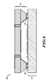
- FIGURE 6 illustrates a side cross-sectional view of a MEMS device in accordance with an embodiment of the present invention.
- the present invention provides microelectromechanical sensor (MEMS) devices and fabrication processing methods for improving production yield by hermetically sealing a MEMS device with a hermetic interface chip (HIC) at the wafer level. Additionally, the MEMS devices and packaging techniques of the present invention eliminate almost all problems associated with presently available Wafer Level Packaging (WLP) techniques by hermetically sealing a MEMS device with an additional wafer, the HIC.
- FIGURE 1 illustrates a side cross-sectional view of a hermetically sealed MEMS device 10 in accordance with an embodiment of the invention.
- the MEMS device 10 includes a HIC 11 having an upper substrate layer 12, feedthrough vias 28, an outer seal ring 18, and etched substrate mesas 20; and a device component 15 having an upper substrate layer 14, a mechanism device layer 32, and a lower substrate layer 16 with bond pads 34.
- the HIC 11 further includes internal 26 and external 30 conductive leads connecting through the feedthrough vias 28, at least one getter component 24, and conductive interconnecting agents 22 disposed at the lower end of the etched substrate mesas 20.
- the HIC 11 facilitates connection of the mechanism device layer 32 of the MEMS device 10 with the external leads 30 outside of the MEMS device during a hermetic sealing process.
- conductive interconnecting agents 22 are bonded to bond pads 34 to connect leads (not shown) emanating from the mechanism device layer 32 with the internal leads 26 disposed on the surface of the etched substrate mesas 20.
- the internal leads 26 on the substrate mesas 20 connect to the external leads 30 through a conductive trace included in the feedthrough vias 28.
- the external leads 30 are made available for new packaging technologies such as flip-chip construction.
- the HIC 11 can act as an interface for additional chips such as analog application specific integrated circuits (ASIC) or digital signal processors (DSP).
- ASIC application specific integrated circuits
- DSP digital signal processors
- the etched substrate mesas 20 are formed of silicon and are pyramidal in shape. These mesas 20 are designed to fit inside of fabricated holes (e.g., ultrasonically drilled holes) in the upper substrate layer 14 of the device component 15.
- the upper substrate layer 14 and the lower substrate layer 16 of the device component 15 are formed of glass.
- the upper substrate layer 12 of the HIC 11 can be formed of either glass or silicon.
- the internal leads 26 of the HIC 11 are patterned on the etched substrate mesas 20 to line up with the bond pads 34 on the lower substrate layer 16 of the device component 15.
- each internal lead 26 disposed on the surface of an etched substrate mesa 20 terminates with the interconnecting agent 22, which is a solder ball that can be reflowed onto a bond pad 34 during a bonding process.
- the other end of the internal lead 26 terminates at the feedthrough vias 28.
- the outer seal ring 18 forms a continuous solder seal ring around the etched substrate mesas 20 and the at least one getter component 24.
- the solder ring hermetically seals around all openings between the upper substrate layer 12 of the HIC 11 and the upper substrate layer 14 of the device component 15. Because the feedthrough vias 28 go from the cavity space between the HIC 11 and the device component 15, through the upper substrate layer 12 of the HIC 11, rather than through the outer seal ring 18, there is no opportunity for electrical shorts or parasitics to occur.
- metal bond pads can be patterned onto or near the feedthrough vias 28 on the top side of the upper substrate layer 12 of the HIC 11. These bond pads can be wire bonded to an external board or circuit such as an ASIC or DSP. In another embodiment, bump bonding balls are placed on the external leads 30 for flip chip bonding to an external board or circuit.
- FIGURE 2 illustrates a bottom view of the HIC 40 in accordance with an embodiment of the present invention.
- the underside of the HIC 40 includes multiple etched substrate mesas 20, multiple getter components 24, the outer seal ring 18, and multiple feedthrough vias 28 connected to the conductive interconnecting agents 22, across the surface of the etched substrate mesas 20, with the internal leads 26.
- FIGURE 3 illustrates a side view of the MEMS device 50 during a fabrication processing step in accordance with an embodiment of the invention.
- the HIC 11 is bonded to the upper substrate layer 14 of the device component 15 with the outer seal ring 18 on the upper substrate layer 12 of the HIC 11.
- conductive interconnecting agents 22 on the surface of the etched substrate mesas 20 are bonded to the bond pads 34 on the lower substrate layer 16 of the device component 15, thereby creating a conductive path from the mechanism device layer 32 to the external conductive leads 30.
- FIGURE 4 illustrates an embodiment of the invention where a MEMS device 60 includes integrated electronics 36 in the upper substrate layer 12 of an HIC 11.
- the HIC 11 is formed of silicon and the integrated electronics 36 can be directly integrated into the silicon substrate. This integration can eliminate one or two levels of interconnections (e.g., wire or bump bonds), along with the noise and parasitics that typically accompany such interconnects.
- the integrated electronics 36 include analog and/or digital components. Further, although the integrated electronics 36 are shown on the upper side of the HIC 11 (the non-mesa side), they could just as easily be integrated into the mesa side of the HIC 11.
- placement of the integrated electronics inside the cavity of the MEMS device 60 could advantageously eliminate another level of external interconnection.
- the integrated electronics 36 would need to be fabricated on a planar wafer, before bonding with the mesa wafer, or after bonding the mesa wafer but before etching the mesas 20. Aside from these modifications, the process would essentially remain the same as described above (i.e., the MEMS fabrication process where the HIC 11 is formed of a silicon substrate). Integrating electronics into the silicon substrate in this process would put limits on the maximum processing temperature (e.g., 450° C), but all the HIC process steps can be done at a lower temperature than that.
- the maximum processing temperature e.g., 450° C
- FIGURE 5 illustrates another embodiment of an HIC 11 of a MEMS device 70, where feedthrough vias 28 feed directly through the etched substrate mesas 20.
- feedthrough vias 28 feed directly through the etched substrate mesas 20.
- the internal leads 26 there is no need for the internal leads 26 to be patterned on the mesas 20.
- the conductive traces of the feedthrough vias 28 terminate directly with interconnecting agents 22, which line up with the bond pads 34 on the lower substrate layer 16 of the device component 15.
- FIGURE 6 illustrates another embodiment of a device component 15 in a MEMS device 80.
- the device component 15 does not include the upper substrate layer 14.
- the regions at the periphery of the lower substrate layer 16 are not covered by the mechanism device layer 32 and can be a hermetically sealed with the HIC 11 at the outer seal ring 18.
- An example MEMS fabrication process for forming multiple MEMS devices in accordance with an embodiment of the present invention forms the upper substrate layer 12 of a HIC 11 of a silicon substrate which can be hermetically bonded with the upper substrate layer 14 of the device component 15. This process includes the following steps:
- An example of a MEMS fabrication process for forming multiple MEMS devices in accordance with another embodiment of the present invention includes an HIC formed of a glass substrate that can be hermetically bonded with an upper substrate layer of a device component. This process includes the following steps:
Landscapes
- Engineering & Computer Science (AREA)
- Microelectronics & Electronic Packaging (AREA)
- Computer Hardware Design (AREA)
- Micromachines (AREA)
Applications Claiming Priority (1)
| Application Number | Priority Date | Filing Date | Title |
|---|---|---|---|
| US12/247,368 US20100084752A1 (en) | 2008-10-08 | 2008-10-08 | Systems and methods for implementing a wafer level hermetic interface chip |
Publications (1)
| Publication Number | Publication Date |
|---|---|
| EP2174907A2 true EP2174907A2 (de) | 2010-04-14 |
Family
ID=41606680
Family Applications (1)
| Application Number | Title | Priority Date | Filing Date |
|---|---|---|---|
| EP09171885A Withdrawn EP2174907A2 (de) | 2008-10-08 | 2009-09-30 | System und Verfahren zur Umsetzung eines hermetischen Schnittstellenchips auf Waferebene |
Country Status (4)
| Country | Link |
|---|---|
| US (1) | US20100084752A1 (de) |
| EP (1) | EP2174907A2 (de) |
| JP (1) | JP2010093257A (de) |
| KR (1) | KR20100039814A (de) |
Cited By (1)
| Publication number | Priority date | Publication date | Assignee | Title |
|---|---|---|---|---|
| CN106249372A (zh) * | 2016-09-18 | 2016-12-21 | 上海晶鼎光电科技有限公司 | 一种晶圆级集成光学窗口及其制作方法 |
Families Citing this family (18)
| Publication number | Priority date | Publication date | Assignee | Title |
|---|---|---|---|---|
| US8240203B2 (en) * | 2008-12-11 | 2012-08-14 | Honeywell International Inc. | MEMS devices and methods with controlled die bonding areas |
| CN101962166B (zh) * | 2010-08-16 | 2012-07-25 | 苏州晶方半导体科技股份有限公司 | 封装结构以及封装方法 |
| WO2012154165A1 (en) | 2011-05-09 | 2012-11-15 | Hewlett-Packard Development Company, L.P. | Bonded wafer structures |
| US9162303B2 (en) * | 2011-07-21 | 2015-10-20 | Blackberry Limited | Grooved circuit board accommodating mixed-size components |
| US9061884B1 (en) | 2012-04-24 | 2015-06-23 | Amkor Technology, Inc. | Integrated circuit with efficient MEMS architecture |
| US20140038357A1 (en) * | 2012-08-06 | 2014-02-06 | Apple Inc. | Singulated ic stiffener and de-bond process |
| US9059161B2 (en) | 2012-09-20 | 2015-06-16 | International Business Machines Corporation | Composite wiring board with electrical through connections |
| CN104037135B (zh) * | 2013-03-07 | 2017-09-22 | 精材科技股份有限公司 | 晶片封装体及其形成方法 |
| ITTO20130350A1 (it) * | 2013-04-30 | 2014-10-31 | St Microelectronics Srl | Assemblaggio a livello di fetta di un dispositivo sensore mems e relativo dispositivo sensore mems |
| WO2015013827A1 (en) | 2013-08-02 | 2015-02-05 | Motion Engine Inc. | Mems motion sensor for sub-resonance angular rate sensing |
| DE102013222583B4 (de) | 2013-11-07 | 2024-06-20 | Robert Bosch Gmbh | Mikromechanische Sensorvorrichtung und entsprechendes Herstellungsverfahren |
| US20170030788A1 (en) | 2014-04-10 | 2017-02-02 | Motion Engine Inc. | Mems pressure sensor |
| US11674803B2 (en) | 2014-06-02 | 2023-06-13 | Motion Engine, Inc. | Multi-mass MEMS motion sensor |
| US11287486B2 (en) | 2014-12-09 | 2022-03-29 | Motion Engine, Inc. | 3D MEMS magnetometer and associated methods |
| US10407299B2 (en) | 2015-01-15 | 2019-09-10 | Motion Engine Inc. | 3D MEMS device with hermetic cavity |
| US10107662B2 (en) | 2015-01-30 | 2018-10-23 | Honeywell International Inc. | Sensor assembly |
| FI20205914A1 (en) * | 2020-09-21 | 2022-03-22 | Teknologian Tutkimuskeskus Vtt Oy | Wafer level package for device |
| CN117242567A (zh) * | 2021-05-12 | 2023-12-15 | 三菱电机株式会社 | 气密封装元件以及元件模块 |
Family Cites Families (9)
| Publication number | Priority date | Publication date | Assignee | Title |
|---|---|---|---|---|
| US6040618A (en) * | 1997-03-06 | 2000-03-21 | Micron Technology, Inc. | Multi-chip module employing a carrier substrate with micromachined alignment structures and method of forming |
| US6818464B2 (en) * | 2001-10-17 | 2004-11-16 | Hymite A/S | Double-sided etching technique for providing a semiconductor structure with through-holes, and a feed-through metalization process for sealing the through-holes |
| TW560018B (en) * | 2001-10-30 | 2003-11-01 | Asia Pacific Microsystems Inc | A wafer level packaged structure and method for manufacturing the same |
| US6635509B1 (en) * | 2002-04-12 | 2003-10-21 | Dalsa Semiconductor Inc. | Wafer-level MEMS packaging |
| US7138293B2 (en) * | 2002-10-04 | 2006-11-21 | Dalsa Semiconductor Inc. | Wafer level packaging technique for microdevices |
| US20040259325A1 (en) * | 2003-06-19 | 2004-12-23 | Qing Gan | Wafer level chip scale hermetic package |
| US7291513B2 (en) * | 2003-12-15 | 2007-11-06 | Dalsa Semiconductor Inc. | Hermetic wafer-level packaging for MEMS devices with low-temperature metallurgy |
| US7115436B2 (en) * | 2004-02-12 | 2006-10-03 | Robert Bosch Gmbh | Integrated getter area for wafer level encapsulated microelectromechanical systems |
| US7402905B2 (en) * | 2006-08-07 | 2008-07-22 | Honeywell International Inc. | Methods of fabrication of wafer-level vacuum packaged devices |
-
2008
- 2008-10-08 US US12/247,368 patent/US20100084752A1/en not_active Abandoned
-
2009
- 2009-09-30 EP EP09171885A patent/EP2174907A2/de not_active Withdrawn
- 2009-10-06 JP JP2009232400A patent/JP2010093257A/ja not_active Withdrawn
- 2009-10-07 KR KR1020090095140A patent/KR20100039814A/ko not_active Withdrawn
Cited By (1)
| Publication number | Priority date | Publication date | Assignee | Title |
|---|---|---|---|---|
| CN106249372A (zh) * | 2016-09-18 | 2016-12-21 | 上海晶鼎光电科技有限公司 | 一种晶圆级集成光学窗口及其制作方法 |
Also Published As
| Publication number | Publication date |
|---|---|
| KR20100039814A (ko) | 2010-04-16 |
| US20100084752A1 (en) | 2010-04-08 |
| JP2010093257A (ja) | 2010-04-22 |
Similar Documents
| Publication | Publication Date | Title |
|---|---|---|
| EP2174907A2 (de) | System und Verfahren zur Umsetzung eines hermetischen Schnittstellenchips auf Waferebene | |
| US10093533B2 (en) | CMOS-MEMS-CMOS platform | |
| CN105967137B (zh) | 为晶圆级芯片尺寸封装件(wlcsp)应用缓解焊接偏移的结构和方法 | |
| TWI502705B (zh) | 晶片封裝體及其製造方法 | |
| US10882738B2 (en) | Wafer level package for a mems sensor device and corresponding manufacturing process | |
| US9862593B2 (en) | MEMS-CMOS device that minimizes outgassing and methods of manufacture | |
| US9919915B2 (en) | Method and system for MEMS devices with dual damascene formed electrodes | |
| CN101243010A (zh) | 微部件的芯片级封装 | |
| US10988373B2 (en) | MEMS component having low-resistance wiring and method for manufacturing it | |
| CN107697882B (zh) | 用于制造半导体器件的工艺以及相应半导体器件 | |
| CN102050418B (zh) | 一种三维集成结构及其生产方法 | |
| EP2266920A2 (de) | Interfacedeckel für hermetische MEMS-Verkapselung | |
| CN118660860A (zh) | 集成电路封装集成的应力隔离 | |
| CN103224217A (zh) | 用于导电柱的系统和方法 | |
| CN101987719B (zh) | 感测元件结构与制造方法 |
Legal Events
| Date | Code | Title | Description |
|---|---|---|---|
| PUAI | Public reference made under article 153(3) epc to a published international application that has entered the european phase |
Free format text: ORIGINAL CODE: 0009012 |
|
| 17P | Request for examination filed |
Effective date: 20090930 |
|
| AK | Designated contracting states |
Kind code of ref document: A2 Designated state(s): AT BE BG CH CY CZ DE DK EE ES FI FR GB GR HR HU IE IS IT LI LT LU LV MC MK MT NL NO PL PT RO SE SI SK SM TR |
|
| AX | Request for extension of the european patent |
Extension state: AL BA RS |
|
| STAA | Information on the status of an ep patent application or granted ep patent |
Free format text: STATUS: THE APPLICATION HAS BEEN WITHDRAWN |
|
| 18W | Application withdrawn |
Effective date: 20120517 |