EP2175494A2 - Verbundhalbleiterbauelement und Herstellungsverfahren dafür - Google Patents
Verbundhalbleiterbauelement und Herstellungsverfahren dafür Download PDFInfo
- Publication number
- EP2175494A2 EP2175494A2 EP09178269A EP09178269A EP2175494A2 EP 2175494 A2 EP2175494 A2 EP 2175494A2 EP 09178269 A EP09178269 A EP 09178269A EP 09178269 A EP09178269 A EP 09178269A EP 2175494 A2 EP2175494 A2 EP 2175494A2
- Authority
- EP
- European Patent Office
- Prior art keywords
- layer
- compound semiconductor
- semiconductor device
- forming
- gate electrode
- Prior art date
- Legal status (The legal status is an assumption and is not a legal conclusion. Google has not performed a legal analysis and makes no representation as to the accuracy of the status listed.)
- Granted
Links
Images






Classifications
-
- H—ELECTRICITY
- H10—SEMICONDUCTOR DEVICES; ELECTRIC SOLID-STATE DEVICES NOT OTHERWISE PROVIDED FOR
- H10D—INORGANIC ELECTRIC SEMICONDUCTOR DEVICES
- H10D30/00—Field-effect transistors [FET]
- H10D30/40—FETs having zero-dimensional [0D], one-dimensional [1D] or two-dimensional [2D] charge carrier gas channels
- H10D30/47—FETs having zero-dimensional [0D], one-dimensional [1D] or two-dimensional [2D] charge carrier gas channels having two-dimensional [2D] charge carrier gas channels, e.g. nanoribbon FETs or high electron mobility transistors [HEMT]
-
- H—ELECTRICITY
- H10—SEMICONDUCTOR DEVICES; ELECTRIC SOLID-STATE DEVICES NOT OTHERWISE PROVIDED FOR
- H10D—INORGANIC ELECTRIC SEMICONDUCTOR DEVICES
- H10D30/00—Field-effect transistors [FET]
- H10D30/01—Manufacture or treatment
- H10D30/015—Manufacture or treatment of FETs having heterojunction interface channels or heterojunction gate electrodes, e.g. HEMT
-
- H—ELECTRICITY
- H10—SEMICONDUCTOR DEVICES; ELECTRIC SOLID-STATE DEVICES NOT OTHERWISE PROVIDED FOR
- H10D—INORGANIC ELECTRIC SEMICONDUCTOR DEVICES
- H10D30/00—Field-effect transistors [FET]
- H10D30/40—FETs having zero-dimensional [0D], one-dimensional [1D] or two-dimensional [2D] charge carrier gas channels
- H10D30/47—FETs having zero-dimensional [0D], one-dimensional [1D] or two-dimensional [2D] charge carrier gas channels having two-dimensional [2D] charge carrier gas channels, e.g. nanoribbon FETs or high electron mobility transistors [HEMT]
- H10D30/471—High electron mobility transistors [HEMT] or high hole mobility transistors [HHMT]
- H10D30/475—High electron mobility transistors [HEMT] or high hole mobility transistors [HHMT] having wider bandgap layer formed on top of lower bandgap active layer, e.g. undoped barrier HEMTs such as i-AlGaN/GaN HEMTs
- H10D30/4755—High electron mobility transistors [HEMT] or high hole mobility transistors [HHMT] having wider bandgap layer formed on top of lower bandgap active layer, e.g. undoped barrier HEMTs such as i-AlGaN/GaN HEMTs having wide bandgap charge-carrier supplying layers, e.g. modulation doped HEMTs such as n-AlGaAs/GaAs HEMTs
-
- H—ELECTRICITY
- H10—SEMICONDUCTOR DEVICES; ELECTRIC SOLID-STATE DEVICES NOT OTHERWISE PROVIDED FOR
- H10D—INORGANIC ELECTRIC SEMICONDUCTOR DEVICES
- H10D62/00—Semiconductor bodies, or regions thereof, of devices having potential barriers
- H10D62/80—Semiconductor bodies, or regions thereof, of devices having potential barriers characterised by the materials
- H10D62/82—Heterojunctions
-
- H—ELECTRICITY
- H10—SEMICONDUCTOR DEVICES; ELECTRIC SOLID-STATE DEVICES NOT OTHERWISE PROVIDED FOR
- H10D—INORGANIC ELECTRIC SEMICONDUCTOR DEVICES
- H10D62/00—Semiconductor bodies, or regions thereof, of devices having potential barriers
- H10D62/80—Semiconductor bodies, or regions thereof, of devices having potential barriers characterised by the materials
- H10D62/82—Heterojunctions
- H10D62/824—Heterojunctions comprising only Group III-V materials heterojunctions, e.g. GaN/AlGaN heterojunctions
-
- H—ELECTRICITY
- H10—SEMICONDUCTOR DEVICES; ELECTRIC SOLID-STATE DEVICES NOT OTHERWISE PROVIDED FOR
- H10D—INORGANIC ELECTRIC SEMICONDUCTOR DEVICES
- H10D62/00—Semiconductor bodies, or regions thereof, of devices having potential barriers
- H10D62/80—Semiconductor bodies, or regions thereof, of devices having potential barriers characterised by the materials
- H10D62/85—Semiconductor bodies, or regions thereof, of devices having potential barriers characterised by the materials being Group III-V materials, e.g. GaAs
- H10D62/8503—Nitride Group III-V materials, e.g. AlN or GaN
-
- H—ELECTRICITY
- H10—SEMICONDUCTOR DEVICES; ELECTRIC SOLID-STATE DEVICES NOT OTHERWISE PROVIDED FOR
- H10D—INORGANIC ELECTRIC SEMICONDUCTOR DEVICES
- H10D64/00—Electrodes of devices having potential barriers
- H10D64/60—Electrodes characterised by their materials
- H10D64/66—Electrodes having a conductor capacitively coupled to a semiconductor by an insulator, e.g. MIS electrodes
- H10D64/68—Electrodes having a conductor capacitively coupled to a semiconductor by an insulator, e.g. MIS electrodes characterised by the insulator, e.g. by the gate insulator
- H10D64/693—Electrodes having a conductor capacitively coupled to a semiconductor by an insulator, e.g. MIS electrodes characterised by the insulator, e.g. by the gate insulator the insulator comprising nitrogen, e.g. nitrides, oxynitrides or nitrogen-doped materials
Definitions
- the present invention relates to a compound semiconductor device suitable for a high electron mobility transistor (HEMT) and so on and a manufacturing method thereof.
- HEMT high electron mobility transistor
- an electronic device (a compound semiconductor device) is vigorous in which a GaN layer and an AlGaN layer are formed sequentially on a substrate composed of sapphire, SiC, GaN, Si, or the like, and the GaN layer is used as an electron transit layer.
- a bandgap of GaN is 3.4 eV, and it is larger than that of GaAs of 1.4 eV. Accordingly, an operation in high withstand voltage is expected for the compound semiconductor device.
- a high-voltage operation is required for a base station amplifier of a cellular phone system, and a high withstand voltage is essential requirement thereof. At present, a value over 300 V is reported as a withstand voltage when current is turned off. There is a case when a change in on-resistance during operation called as a current collapse occurs in the above-stated compound semiconductor device. This phenomenon can be avoided by disposing a GaN protective layer on an AlGaN electron supply layer, and further forming an SiN protective film. The structure as stated above is described in, for example, Patent Document 1.
- Fig. 16 is a sectional view showing a structure of a conventional compound semiconductor device.
- An AlN layer 102, a GaN layer 103, an n-type AlGaN layer 104a, an n-type AlGaN layer 104b and an n-type GaN layer 105 are sequentially formed on an SiC substrate 101.
- a thickness of the AlN layer 102 is 150 ⁇ m.
- a total thickness of the n-type AlGaN layer 104b and the n-type GaN layer 105 is approximately 30 nm.
- an SiN layer 107 is formed on the n-type GaN layer 105.
- Plural openings are formed at the SiN layer 107, and a source electrode 108a, a drain electrode 108b and a gate electrode 109 are evaporated in these openings.
- this compound semiconductor device is a normally-on type.
- a compound semiconductor device is used for automobile parts. Current continues to flow in the automobile parts when a car goes out of order resulting from a traffic accident and so on when the compound semiconductor device is the normally-on type. Accordingly, a demand for a normally-off type compound semiconductor device becomes high in recent times.
- a positive gate leakage current flows in a saturation region as input power is made large. This is because the gate electrode 109 and the n-type GaN layer 105 are in contact directly. It is difficult to continue to use in a saturation power state if the gate leak current as stated above flows, and it is hard to say that it is suitable for the base station amplifier of the cellular phone.
- An object of the present invention is to provide a compound semiconductor device and a manufacturing method thereof capable of suppressing current flowing when a gate voltage is set to be "0" (zero), and manufacturing with high reproducibility.
- a GaN based carrier transit layer is formed on a semiconductor substrate, a GaN based carrier supply layer is formed on the carrier transit layer, a GaN based protective layer is formed on the carrier supply layer, and a source electrode, a drain electrode and a gate electrode are formed on the protective layer.
- a compound semiconductor layer containing nitrogen and positioning between the gate electrode and the source electrode, and between the gate electrode and the drain electrode, is formed on the protective layer, and an insulator layer is formed on the compound semiconductor layer.
- a GaN based carrier transit layer is formed on a semiconductor substrate, and thereafter, a GaN based carrier supply layer is formed on the carrier transit layer.
- a GaN based protective layer is formed on the carrier supply layer.
- a compound semiconductor layer containing nitrogen is formed on the protective layer.
- an insulator layer is formed on the compound semiconductor layer.
- an opening for a source electrode, an opening for a drain electrode and an opening for a gate electrode are formed in the insulator layer and the compound semiconductor layer.
- electrodes are formed in the three openings. In forming the opening for a gate electrode, wet etching of the compound semiconductor layer is performed until the protective layer exposes.
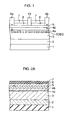
- FIG. 1 is a sectional view showing a structure of a compound semiconductor device according to the first embodiment of the present invention.
- an AlN layer 2 with a thickness of approximately 150 nm to 300 nm is formed on an SiC substrate 1.
- a GaN buffer layer 3 (a carrier transit layer) with a thickness of approximately 3 ⁇ m is formed on the AlN layer 2.
- a non-doped AlGaN layer 4a with a thickness of approximately 5 nm is formed on the GaN buffer layer 3.
- An n-type AlGaN layer 4b (a carrier supply layer) with a thickness of approximately 15 nm to 20 nm is formed on the non-doped AlGaN layer 4a.
- the n-type AlGaN layer 4b is doped with Si at approximately 4 ⁇ 10 18 cm -3 .
- an n-type GaN layer 5 (a protective layer) with a thickness of approximately 7 nm is formed on the n-type AlGaN layer 4b.
- the n-type GaN layer 5 is doped with Si at approximately 5 ⁇ 10 18 cm -3 .
- a non-doped AlN layer 6 with a thickness of approximately 3 nm and an SiN layer 7 with a thickness of approximately 20 nm are sequentially formed on the n-type GaN layer 5.
- a semiconductor-insulator junction exists between the non-doped AlN layer 6 and the SiN layer 7.
- At least three openings are formed in the non-doped AlN layer 6 and the SiN layer 7, and a source electrode 8a, a drain electrode 8b and a gate electrode 19 are evaporated in these openings.
- a semiconductor-metal junction exists between the non-doped AlN layer 6 and the gate electrode 19.
- a metal-semiconductor junction exists between the gate electrode 19 and the n-type GaN layer 5.
- the source electrode 8a and the drain electrode 8b may be composed of, for example, a Ta film with a thickness of approximately 10 nm and an Al film with a thickness of approximately 300 nm formed thereon.
- the gate electrode 19 may be composed of, for example, an Ni film and an Au film formed thereon.
- a piezoelectric effect resulting from a lattice mismatch occurs in a vicinity of an interface of the non-doped AlGaN layer 4a with the GaN buffer layer 3. Accordingly, positive polarization charges appear, and electrons are induced in the vicinity of the interface of the GaN buffer layer 3 with the non-doped AlGaN layer 4a. As a result, a two-dimensional electron gas (2DEG) appears.
- 2DEG two-dimensional electron gas
- the SiN layer 7 exists at a periphery of the gate electrode 19 as an insulator layer, and therefore, it is possible to prevent a gate leak current from a side surface. Accordingly, a high withstand voltage is realized.
- the non-doped AlN layer 6 exists between the SiN layer 7 and the n-type GaN layer 5, and therefore, electrons exist at an interface between the non-doped AlN layer 6 and the n-type GaN layer 5. Accordingly, a lot of two-dimensional electron gas exists at an electron transit region between the gate electrode 19 and the source electrode 8a and the drain electrode 8b. Consequently, a transconductance (Gm) improves, and on-resistance is suppressed to be low. Besides, a threshold voltage approximates to "0" (zero) V more closely because a gate recess structure is adopted. Namely, it becomes possible to secure the enough current while approximating the threshold voltage to "0" (zero) V owing to these interactions.
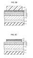
- FIG. 2A to Fig. 2G are sectional views showing the manufacturing method of the compound semiconductor device according to the first embodiment of the present invention in process sequence.
- the AlN layer 2 is formed on the SiC substrate 1, as shown in Fig. 2A .
- the GaN buffer layer 3 is formed on the AlN layer 2.
- the non-doped AlGaN layer 4a is formed on the GaN buffer layer 3.
- the n-type AlGaN layer 4b is formed on the non-doped AlGaN layer 4a.
- the n-type GaN layer 5 is formed on the n-type AlGaN layer 4b.
- the non-doped AlN layer 6 is formed on the n-type GaN layer 5.
- the SiN layer 7 is formed on the non-doped AlN layer 6.
- the formations of the AIN layer 2, the GaN buffer layer 3, the non-doped AlGaN layer 4a, the n-type AlGaN layer 4b, the n-type GaN layer 5 and the non-doped AlN layer 6 may be performed by, for example, a crystal growth method such as an MOCVD method.
- the formation of the SiN layer 7 may be performed by, for example, a plasma CVD method.
- a resist pattern 21 having openings at regions where the source electrode 8a and the drain electrode 8b are to be formed is formed on the SiN layer 7, as shown in Fig. 2B .
- wet etching of the SiN layer 7 and the non-doped AlN layer 6 is performed by using the resist pattern 21 as a mask, and thereby, the opening for the source electrode and the opening for the drain electrode are formed in the SiN layer 7 and the non-doped AlN layer 6, as shown in Fig. 2C .
- the n-type GaN layer 5 positioning under the non-doped AlN layer 6 is not removed by the wet etching, and therefore, the etching is stopped at a surface of the n-type GaN layer 5.
- the resist pattern 21 is removed after the openings are formed.
- the source electrode 8a and the drain electrode 8b are evaporated in the openings in the SiN layer 7 and the non-doped AlN layer 6, as shown in Fig. 2D .
- a resist pattern 22 having an opening at a region where the gate electrode 19 is to be formed is formed on the SiN layer 7, the source electrode 8a and the drain electrode 8b, as shown in Fig. 2E .
- wet etching etching using acid
- wet etching using acid of the SiN layer 7 and the non-doped AlN layer 6 is performed by using the resist pattern 22 as a mask, and thereby, the opening for the gate electrode is formed in the SiN layer 7 and the non-doped AlN layer 6, as shown in Fig. 2F .
- the n-type GaN layer 5 positioning under the non-doped AlN layer 6 is not removed by the wet etching, and therefore, the etching is stopped at the surface of the n-type GaN layer 5.
- the resist pattern 22 is removed after the opening is formed.
- the gate electrode 19 (an embedded gate electrode) is evaporated in the opening in the SiN layer 7 and the non-doped AlN layer 6, as shown in Fig. 2G .
- element isolation can be performed by, for example, ion-implantation, though it is not shown.
- a selection ratio between the non-doped AlN layer 6 and the n-type GaN layer 5 at the wet etching is high, and therefore, it is possible to process the non-doped AlN layer 6 with high accuracy. Accordingly, it is possible to form the gate electrode 19 having good reproducibility with high accuracy.
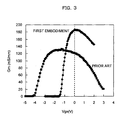
- Fig. 3 is a graphic chart showing the device characteristic of the compound semiconductor device according to the first embodiment measured by the present inventor.
- a device characteristic of the conventional compound semiconductor device shown in Fig. 16 is also shown in Fig. 3 for the purpose of reference.
- a horizontal axis is a voltage between gate-source (Vgs), and a vertical axis is a transconductance (Gm).
- Vgs gate-source
- Gm transconductance
- the threshold voltage approximates to "0" (zero) V more closely in the first embodiment compared to the conventional compound semiconductor device.
- bottom surfaces of the source electrode 8a and the drain electrode 8b are in contact with the surface of the n-type GaN layer 5, but they may be in contact with a surface of the n-type AlGaN layer 4b as shown in Fig. 15 .
- the opening for the source electrode and the opening for the drain electrode are formed in the SiN layer 7 and the non-doped AlN layer 6 by using the resist pattern 21 shown in Fig. 2B as the mask, and thereafter, a dry etching of the n-type GaN layer 5 is performed while remaining the resist pattern 21.
- a reactive ion etching is performed, for example, with a pressure of 2 Pa, a Cl 2 flow rate of 10 sccm, and an etching speed of 10 nm/min.
- An end point of the dry etching may be determined by, for example, a time control.
- an error of an etching amount is preferable to be within ⁇ 3 nm.
- the source electrode 8a and the drain electrode 8b may be composed of, for example, a Ta film with a thickness of approximately 10 nm and an Al film with a thickness of approximately 300 nm formed thereon.
- FIG. 4 is a sectional view showing a structure of a compound semiconductor device according to the second embodiment of the present invention.
- the opening for the gate electrode of the non-doped AlN layer 6 is approximately equal to that of the first embodiment, the opening for the gate electrode of the SiN layer 7 is wider than that of the first embodiment.
- a gate electrode 29 having an overhang portion is embedded in the opening.
- the other structure is the same as the first embodiment.
- an electric field concentration in a vicinity of an interface between the gate electrode 29 and the non-doped AlN layer 6 is reduced than the electric field concentration in a vicinity of an interface between the gate electrode 19 and the non-doped AlN layer 6 in the first embodiment.
- a voltage of 50 V to 500 V is applied between the gate and drain in the compound semiconductor device, but according to the second embodiment, deterioration hardly occurs furthermore even in the case as stated above.
- FIG. 5A to Fig. 5C are sectional views showing the manufacturing method of the compound semiconductor device according to the second embodiment of the present invention in process sequence.
- a resist pattern 23 having an opening at a region where the overhang portion of the gate electrode 29 is to be formed is formed on the SiN layer 7, the source electrode 8a and the drain electrode 8b, as shown in Fig. 5A .
- wet etching of the SiN layer 7 is performed by using the resist pattern 23 as a mask, and thereby, the opening for the overhang portion is formed in the SiN layer 7, as shown in Fig. 5B .
- the resist pattern 23 is removed after the opening is formed.
- the gate electrode 29 (an embedded gate electrode) is evaporated in the opening in the SiN layer 7 and the non-doped AlN layer 6, as shown in Fig. 5C .
- element isolation can be performed by, for example, ion-implantation, though it is not shown.
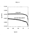
- Fig. 6 is a graphic chart showing the device characteristic of the compound semiconductor device according to the second embodiment measured by the present inventor.
- a device characteristic of the conventional compound semiconductor device shown in Fig. 16 is also shown for the purpose of reference.
- a horizontal axis is a voltage between gate-drain (Vgd), and a vertical axis is a current between gate-drain (Igd).
- Vgd gate-drain
- Igd current between gate-drain
- a backward gate leak current decreases in the second embodiment compared to the conventional compound semiconductor device.
- the threshold voltage approximates to "0" (zero) V without decreasing saturation current.
- a third embodiment of the present invention is described.
- an MIS (Metal-Insulator-Semiconductor) structure is adopted.
- Fig. 7 is a sectional view showing the structure of a compound semiconductor device according to the third embodiment of the present invention.
- an SiN layer 7a with a thickness of approximately 10 nm is formed on the non-doped AlN layer 6. At least three openings (for a source electrode, for a drain electrode and for a gate electrode) are formed in the non-doped AlN layer 6 and the SiN layer 7a. In the present embodiment, an SiN layer 7b with a thickness of approximately 10 nm is formed in the opening for the gate electrode among the three openings, and on the SiN layer 7a. A gate electrode 39 having an overhang portion is evaporated in the opening for the gate electrode.
- the other structure is the same as the first embodiment.
- a forward gate leak current can be drastically reduced. Besides, a complete normally-off operation can be performed. Besides, it becomes possible to obtain high current because the normally-off operation is realized.
- FIG. 8A to Fig. 8E are sectional views showing the manufacturing method of the compound semiconductor device according to the third embodiment of the present invention in process sequence.
- the processes until the formation of the non-doped AlN layer 6 are performed as same as the first embodiment.
- the SiN layer 7a is formed on the non-doped AlN layer 6, as shown in Fig. 8A .
- the formation of the SiN layer 7a may be performed by, for example, a plasma CVD method.
- a resist pattern 24 having an opening at a region where a lower portion of the gate electrode 39 is to be formed is formed on the SiN layer 7a, the source electrode 8a and the drain electrode 8b, as shown in Fig. 8B .
- wet etching of the SiN layer 7a and the non-doped AlN layer 6 is performed by using the resist pattern 24 as a mask, and thereby, the opening for the gate electrode is formed in the SiN layer 7a and the non-doped AlN layer 6, as shown in Fig. 8C .
- the n-type GaN layer 5 positioning under the non-doped AlN layer 6 is not removed by the wet etching, and therefore, the etching is stopped at the surface of the n-type GaN layer 5.
- the resist pattern 24 is removed after the opening is formed.
- the SiN layer 7b is formed in the opening for the gate electrode and on the SiN layer 7a, as shown in Fig. 8D .
- the formation of the SiN layer 7b may be performed by, for example, a plasma CVD method.
- the gate electrode 39 (an embedded gate electrode) is evaporated in the opening in the SiN layer 7a and the non-doped AlN layer 6, as shown in Fig. 8E .
- element isolation can be performed by, for example, ion-implantation, though it is not shown.
- Fig. 9 is a graphic chart showing the device characteristic of the compound semiconductor device according to the third embodiment measured by the present inventor.
- a device characteristic of the conventional compound semiconductor device shown in Fig. 16 is also shown for the purpose of reference.
- a horizontal axis is a gate voltage
- a vertical axis is a forward gate leak current.
- the forward gate leak current is reduced in the third embodiment compared to the conventional compound semiconductor device. Namely, in the third embodiment, the gate leak current scarcely flows even when the gate voltage is increased up to approximately 4 V.
- a threshold voltage Vth, a variation thereof ⁇ Vth and a maximum current Imax of the compound semiconductor device manufactured by the present inventor in accordance with the above-stated method are shown in Table 1.
- device characteristics of the conventional compound semiconductor device shown in Fig. 16 are also shown for the purpose of reference.
- the threshold voltage Vth is a negative value in the conventional compound semiconductor device
- the threshold voltage Vth is a positive value in the third embodiment.
- the variation ⁇ Vth of the threshold voltage in the third embodiment is approximately 1/10 of the conventional compound semiconductor device. This is because it is possible to form the structure in the vicinity of the gate electrode 39 with high reproducibility in the third embodiment, but the reproducibility is low in the conventional compound semiconductor device.
- the maximum current Imax becomes extremely high compared to the conventional compound semiconductor device in accordance with the reduction of the gate leak current.
- FIG. 10 is a sectional view showing a structure of a compound semiconductor device according to the fourth embodiment of the present invention.
- an n-type GaN layer 11 with a thickness of approximately 7 nm is formed between the non-doped AlN layer 6 and the SiN layer 7a.
- the n-type GaN layer 11 is doped with Si at approximately 5 ⁇ 10 18 cm -3 .
- An opening similar to those of the non-doped AlN layer 6 and the SiN layer 7a are formed in the n-type GaN layer 11.
- the other structure is the same as the third embodiment.
- a doping amount of Si in the n-type GaN layer 11 may be higher than that of the n-type GaN layer 5.
- the n-type GaN layer 11 is formed on the non-doped AlN layer 6, and therefore, a chemical change of the non-doped AlN layer 6 hardly occurs. Accordingly, deterioration of a whole device hardly occurs, and a high reliability can be obtained.
- the n-type GaN layer 11 is formed on the non-doped AlN layer 6 between the formation of the non-doped AlN layer 6 and the formation of the SiN layer 7a.
- dry etching of the n-type GaN layer 11 is performed. This dry etching may be performed by a time control.
- wet etching of the non-doped AlN layer 6 is performed as same as the first to third embodiments. At this time, the n-type GaN layer 5 positioning under the non-doped AlN layer 6 is not removed by the wet etching, and therefore, the etching is stopped at the surface of the n-type GaN layer 5.
- Fig. 11 is a graphic chart showing a test data of the reliability of the compound semiconductor device according to the fourth embodiment measured by the present inventor.
- test data three kinds of the conventional compound semiconductor device shown in Fig. 16 are shown for the purpose of reference.
- a horizontal axis is test time
- a vertical axis is a gate leak current Ig.
- the gate leak currents are high even at a test start time, and the gate leak currents increase as the time elapses depending on samples, in the conventional compound semiconductor device. This shows that the deterioration is in progress.
- the gate leak current at the test start time is low, and further, the increase in accordance with the elapsed time is not observed at all.
- Fig. 12 is a sectional view showing a structure of a compound semiconductor device according to the fifth embodiment.
- a non-doped GaN layer 12 is formed instead of the n-type GaN layer 5 in the fourth embodiment.
- the non-doped GaN layer 12 is used instead of the n-type GaN layer 5, and therefore, the gate leak current can be reduced further more.
- the MIS structure is adopted as same as the third embodiment, and therefore, the characteristics may not deteriorate even if the non-doped GaN layer 12 is used.
- FIG. 13 is a sectional view showing a structure of a compound semiconductor device according to the sixth embodiment of the present invention.
- an n-type InGaN layer 13 is formed instead of the n-type GaN layer 11 in the fifth embodiment.
- the n-type InGaN layer 13 is used instead of the n-type GaN layer 11, and therefore, a band in this layer decreases, and the two-dimensional electron gas increases. As a result, the maximum current increases.
- Fig. 14 is a sectional view showing a structure of a compound semiconductor device according to the seventh embodiment of the present invention.
- an Si layer 14 for one atomic layer is formed between the non-doped AlN layer 6 and the n-type GaN layer 11 in the fourth embodiment.
- the Si layer 14 may be formed by, for example, a planer doping method (an atomic layer doping method).
- the Si layer 14 may be formed between the n-type GaN layer 5 and the non-doped AlN layer 6.
- the formation of the AlN layer may be performed by an ALD (Atomic Layer Deposition) method, a sputtering method, or the like.
- ALD Atomic Layer Deposition
- the AlN layer is formed between the gate electrode, the source electrode and the drain electrode as a compound semiconductor layer containing N, but another compound semiconductor layer, for example, a layer such as InAlN further containing In may be formed.
- it is described as a simple HEMT, but plural HEMT may be accumulated.
- the element isolation may be performed by, for example, the ion-implantation, a mesa etching, or the like.
- a compound semiconductor layer containing N is formed on a protective layer, and a process of the compound semiconductor layer can be performed under a condition free from an influence on the protective layer. Accordingly, it is possible to construct a gate recess structure with high reproducibility. It is therefore possible to suppress current flowing when a gate voltage is made to be "0" (zero). Besides, it is possible to suppress a gate leak current to realize a high withstand voltage when an insulator layer is in contact with a side surface of a gate electrode.
Landscapes
- Junction Field-Effect Transistors (AREA)
Priority Applications (3)
| Application Number | Priority Date | Filing Date | Title |
|---|---|---|---|
| EP13164123.5A EP2657976B1 (de) | 2006-03-16 | 2006-03-16 | Verbundhalbleiterbauelement und Herstellungsverfahren dafür |
| EP20130164120 EP2677544B1 (de) | 2006-03-16 | 2006-03-16 | Verbindungshalbleiterbauelement und Herstellungsverfahren dafür |
| EP09178269.8A EP2175494B1 (de) | 2006-03-16 | 2006-03-16 | Verbundhalbleiterbauelement und Herstellungsverfahren dafür |
Applications Claiming Priority (3)
| Application Number | Priority Date | Filing Date | Title |
|---|---|---|---|
| PCT/JP2006/305265 WO2007108055A1 (ja) | 2006-03-16 | 2006-03-16 | 化合物半導体装置及びその製造方法 |
| EP06729258A EP1998376B1 (de) | 2006-03-16 | 2006-03-16 | Verbund-halbleiteranordnung und prozess zu ihrer herstellung |
| EP09178269.8A EP2175494B1 (de) | 2006-03-16 | 2006-03-16 | Verbundhalbleiterbauelement und Herstellungsverfahren dafür |
Related Parent Applications (2)
| Application Number | Title | Priority Date | Filing Date |
|---|---|---|---|
| EP06729258A Division EP1998376B1 (de) | 2006-03-16 | 2006-03-16 | Verbund-halbleiteranordnung und prozess zu ihrer herstellung |
| EP06729258.1 Division | 2006-03-16 |
Related Child Applications (4)
| Application Number | Title | Priority Date | Filing Date |
|---|---|---|---|
| EP13164123.5A Division-Into EP2657976B1 (de) | 2006-03-16 | 2006-03-16 | Verbundhalbleiterbauelement und Herstellungsverfahren dafür |
| EP13164123.5A Division EP2657976B1 (de) | 2006-03-16 | 2006-03-16 | Verbundhalbleiterbauelement und Herstellungsverfahren dafür |
| EP20130164120 Division-Into EP2677544B1 (de) | 2006-03-16 | 2006-03-16 | Verbindungshalbleiterbauelement und Herstellungsverfahren dafür |
| EP20130164120 Division EP2677544B1 (de) | 2006-03-16 | 2006-03-16 | Verbindungshalbleiterbauelement und Herstellungsverfahren dafür |
Publications (3)
| Publication Number | Publication Date |
|---|---|
| EP2175494A2 true EP2175494A2 (de) | 2010-04-14 |
| EP2175494A3 EP2175494A3 (de) | 2012-10-17 |
| EP2175494B1 EP2175494B1 (de) | 2015-03-25 |
Family
ID=38522096
Family Applications (5)
| Application Number | Title | Priority Date | Filing Date |
|---|---|---|---|
| EP06729258A Expired - Lifetime EP1998376B1 (de) | 2006-03-16 | 2006-03-16 | Verbund-halbleiteranordnung und prozess zu ihrer herstellung |
| EP09178269.8A Expired - Lifetime EP2175494B1 (de) | 2006-03-16 | 2006-03-16 | Verbundhalbleiterbauelement und Herstellungsverfahren dafür |
| EP20130164120 Expired - Lifetime EP2677544B1 (de) | 2006-03-16 | 2006-03-16 | Verbindungshalbleiterbauelement und Herstellungsverfahren dafür |
| EP09178271A Expired - Lifetime EP2166575B1 (de) | 2006-03-16 | 2006-03-16 | Verbundhalbleiterbauelement |
| EP13164123.5A Expired - Lifetime EP2657976B1 (de) | 2006-03-16 | 2006-03-16 | Verbundhalbleiterbauelement und Herstellungsverfahren dafür |
Family Applications Before (1)
| Application Number | Title | Priority Date | Filing Date |
|---|---|---|---|
| EP06729258A Expired - Lifetime EP1998376B1 (de) | 2006-03-16 | 2006-03-16 | Verbund-halbleiteranordnung und prozess zu ihrer herstellung |
Family Applications After (3)
| Application Number | Title | Priority Date | Filing Date |
|---|---|---|---|
| EP20130164120 Expired - Lifetime EP2677544B1 (de) | 2006-03-16 | 2006-03-16 | Verbindungshalbleiterbauelement und Herstellungsverfahren dafür |
| EP09178271A Expired - Lifetime EP2166575B1 (de) | 2006-03-16 | 2006-03-16 | Verbundhalbleiterbauelement |
| EP13164123.5A Expired - Lifetime EP2657976B1 (de) | 2006-03-16 | 2006-03-16 | Verbundhalbleiterbauelement und Herstellungsverfahren dafür |
Country Status (4)
| Country | Link |
|---|---|
| US (4) | US8344419B2 (de) |
| EP (5) | EP1998376B1 (de) |
| JP (1) | JP5071377B2 (de) |
| WO (1) | WO2007108055A1 (de) |
Families Citing this family (61)
| Publication number | Priority date | Publication date | Assignee | Title |
|---|---|---|---|---|
| JP2008306130A (ja) * | 2007-06-11 | 2008-12-18 | Sanken Electric Co Ltd | 電界効果型半導体装置及びその製造方法 |
| US7915643B2 (en) | 2007-09-17 | 2011-03-29 | Transphorm Inc. | Enhancement mode gallium nitride power devices |
| WO2009066434A1 (ja) * | 2007-11-19 | 2009-05-28 | Nec Corporation | 電界効果トランジスタおよびその製造方法 |
| JP5386829B2 (ja) | 2008-01-30 | 2014-01-15 | 富士通株式会社 | 半導体装置 |
| JP5320774B2 (ja) * | 2008-03-03 | 2013-10-23 | 三菱電機株式会社 | 半導体装置 |
| US8519438B2 (en) | 2008-04-23 | 2013-08-27 | Transphorm Inc. | Enhancement mode III-N HEMTs |
| US8289065B2 (en) | 2008-09-23 | 2012-10-16 | Transphorm Inc. | Inductive load power switching circuits |
| JP5468768B2 (ja) | 2008-12-05 | 2014-04-09 | パナソニック株式会社 | 電界効果トランジスタ及びその製造方法 |
| US7898004B2 (en) | 2008-12-10 | 2011-03-01 | Transphorm Inc. | Semiconductor heterostructure diodes |
| JP5487613B2 (ja) | 2008-12-19 | 2014-05-07 | 富士通株式会社 | 化合物半導体装置及びその製造方法 |
| US8742459B2 (en) | 2009-05-14 | 2014-06-03 | Transphorm Inc. | High voltage III-nitride semiconductor devices |
| JP4794655B2 (ja) * | 2009-06-09 | 2011-10-19 | シャープ株式会社 | 電界効果トランジスタ |
| US8390000B2 (en) | 2009-08-28 | 2013-03-05 | Transphorm Inc. | Semiconductor devices with field plates |
| WO2011033932A1 (ja) * | 2009-09-18 | 2011-03-24 | 株式会社パイオラックス | ホースクランプ |
| JP2011082216A (ja) | 2009-10-02 | 2011-04-21 | Fujitsu Ltd | 化合物半導体装置及びその製造方法 |
| US8389977B2 (en) | 2009-12-10 | 2013-03-05 | Transphorm Inc. | Reverse side engineered III-nitride devices |
| US9378965B2 (en) * | 2009-12-10 | 2016-06-28 | Infineon Technologies Americas Corp. | Highly conductive source/drain contacts in III-nitride transistors |
| CN101916773B (zh) * | 2010-07-23 | 2012-05-23 | 中国科学院上海技术物理研究所 | 一种双沟道mos-hemt器件的制作方法 |
| JP5712583B2 (ja) | 2010-12-02 | 2015-05-07 | 富士通株式会社 | 化合物半導体装置及びその製造方法 |
| JP5724339B2 (ja) * | 2010-12-03 | 2015-05-27 | 富士通株式会社 | 化合物半導体装置及びその製造方法 |
| US8742460B2 (en) | 2010-12-15 | 2014-06-03 | Transphorm Inc. | Transistors with isolation regions |
| JP5654884B2 (ja) * | 2011-01-26 | 2015-01-14 | 株式会社東芝 | 窒化物半導体装置の製造方法 |
| US8643062B2 (en) | 2011-02-02 | 2014-02-04 | Transphorm Inc. | III-N device structures and methods |
| JP5762049B2 (ja) * | 2011-02-28 | 2015-08-12 | ルネサスエレクトロニクス株式会社 | 半導体装置 |
| US8716141B2 (en) | 2011-03-04 | 2014-05-06 | Transphorm Inc. | Electrode configurations for semiconductor devices |
| US8772842B2 (en) | 2011-03-04 | 2014-07-08 | Transphorm, Inc. | Semiconductor diodes with low reverse bias currents |
| GB201112327D0 (en) | 2011-07-18 | 2011-08-31 | Epigan Nv | Method for growing III-V epitaxial layers |
| US8901604B2 (en) | 2011-09-06 | 2014-12-02 | Transphorm Inc. | Semiconductor devices with guard rings |
| US9257547B2 (en) | 2011-09-13 | 2016-02-09 | Transphorm Inc. | III-N device structures having a non-insulating substrate |
| US8598937B2 (en) | 2011-10-07 | 2013-12-03 | Transphorm Inc. | High power semiconductor electronic components with increased reliability |
| US9165766B2 (en) | 2012-02-03 | 2015-10-20 | Transphorm Inc. | Buffer layer structures suited for III-nitride devices with foreign substrates |
| JP2013206976A (ja) * | 2012-03-27 | 2013-10-07 | Fujitsu Ltd | 化合物半導体装置及びその製造方法 |
| WO2013155108A1 (en) | 2012-04-09 | 2013-10-17 | Transphorm Inc. | N-polar iii-nitride transistors |
| US9000484B2 (en) | 2012-05-23 | 2015-04-07 | Hrl Laboratories, Llc | Non-uniform lateral profile of two-dimensional electron gas charge density in type III nitride HEMT devices using ion implantation through gray scale mask |
| US9379195B2 (en) | 2012-05-23 | 2016-06-28 | Hrl Laboratories, Llc | HEMT GaN device with a non-uniform lateral two dimensional electron gas profile and method of manufacturing the same |
| US8680536B2 (en) | 2012-05-23 | 2014-03-25 | Hrl Laboratories, Llc | Non-uniform two dimensional electron gas profile in III-Nitride HEMT devices |
| US10700201B2 (en) | 2012-05-23 | 2020-06-30 | Hrl Laboratories, Llc | HEMT GaN device with a non-uniform lateral two dimensional electron gas profile and method of manufacturing the same |
| US9184275B2 (en) | 2012-06-27 | 2015-11-10 | Transphorm Inc. | Semiconductor devices with integrated hole collectors |
| US8803246B2 (en) | 2012-07-16 | 2014-08-12 | Transphorm Inc. | Semiconductor electronic components with integrated current limiters |
| JP6087552B2 (ja) * | 2012-09-21 | 2017-03-01 | トランスフォーム・ジャパン株式会社 | 化合物半導体装置及びその製造方法 |
| US9583574B2 (en) | 2012-09-28 | 2017-02-28 | Intel Corporation | Epitaxial buffer layers for group III-N transistors on silicon substrates |
| US8884334B2 (en) * | 2012-11-09 | 2014-11-11 | Taiwan Semiconductor Manufacturing Co., Ltd. | Composite layer stacking for enhancement mode transistor |
| JP2014130951A (ja) * | 2012-12-28 | 2014-07-10 | Sumitomo Electric Ind Ltd | 半導体装置 |
| JP6253886B2 (ja) * | 2013-01-09 | 2017-12-27 | トランスフォーム・ジャパン株式会社 | 半導体装置及び半導体装置の製造方法 |
| JP6522521B2 (ja) | 2013-02-15 | 2019-05-29 | トランスフォーム インコーポレーテッド | 半導体デバイスの電極及びその製造方法 |
| US9087718B2 (en) | 2013-03-13 | 2015-07-21 | Transphorm Inc. | Enhancement-mode III-nitride devices |
| US9245992B2 (en) | 2013-03-15 | 2016-01-26 | Transphorm Inc. | Carbon doping semiconductor devices |
| JP5721782B2 (ja) * | 2013-06-26 | 2015-05-20 | パナソニック株式会社 | 半導体装置 |
| US9443938B2 (en) | 2013-07-19 | 2016-09-13 | Transphorm Inc. | III-nitride transistor including a p-type depleting layer |
| KR20150011238A (ko) * | 2013-07-22 | 2015-01-30 | 삼성전자주식회사 | 질화물계 반도체 장치 |
| JP6214978B2 (ja) * | 2013-09-17 | 2017-10-18 | 株式会社東芝 | 半導体装置 |
| US10276712B2 (en) | 2014-05-29 | 2019-04-30 | Hrl Laboratories, Llc | III-nitride field-effect transistor with dual gates |
| US9318593B2 (en) | 2014-07-21 | 2016-04-19 | Transphorm Inc. | Forming enhancement mode III-nitride devices |
| US9536967B2 (en) | 2014-12-16 | 2017-01-03 | Transphorm Inc. | Recessed ohmic contacts in a III-N device |
| US9536966B2 (en) | 2014-12-16 | 2017-01-03 | Transphorm Inc. | Gate structures for III-N devices |
| US9812532B1 (en) | 2015-08-28 | 2017-11-07 | Hrl Laboratories, Llc | III-nitride P-channel transistor |
| ITUB20155503A1 (it) * | 2015-11-12 | 2017-05-12 | St Microelectronics Srl | Metodo di fabbricazione di un transistore hemt e transistore hemt con migliorata mobilita' elettronica |
| CN108292678B (zh) | 2015-11-19 | 2021-07-06 | Hrl实验室有限责任公司 | 具有双栅极的iii族氮化物场效应晶体管 |
| US11322599B2 (en) | 2016-01-15 | 2022-05-03 | Transphorm Technology, Inc. | Enhancement mode III-nitride devices having an Al1-xSixO gate insulator |
| US10224401B2 (en) | 2016-05-31 | 2019-03-05 | Transphorm Inc. | III-nitride devices including a graded depleting layer |
| CN112242441A (zh) * | 2019-07-16 | 2021-01-19 | 联华电子股份有限公司 | 高电子迁移率晶体管 |
Family Cites Families (10)
| Publication number | Priority date | Publication date | Assignee | Title |
|---|---|---|---|---|
| US5888872A (en) | 1997-06-20 | 1999-03-30 | Advanced Micro Devices, Inc. | Method for forming source drain junction areas self-aligned between a sidewall spacer and an etched lateral sidewall |
| US5986209A (en) * | 1997-07-09 | 1999-11-16 | Micron Technology, Inc. | Package stack via bottom leaded plastic (BLP) packaging |
| JP4224737B2 (ja) * | 1999-03-04 | 2009-02-18 | ソニー株式会社 | 半導体素子 |
| JP2002141499A (ja) * | 2000-10-31 | 2002-05-17 | Toshiba Corp | 電界効果トランジスタ及びその製造方法 |
| JP4663156B2 (ja) | 2001-05-31 | 2011-03-30 | 富士通株式会社 | 化合物半導体装置 |
| EP2267784B1 (de) * | 2001-07-24 | 2020-04-29 | Cree, Inc. | AlGaN/GaN HEMT MIT ISOLIERTEM GATE |
| JP3940699B2 (ja) * | 2003-05-16 | 2007-07-04 | 株式会社東芝 | 電力用半導体素子 |
| WO2006001369A1 (ja) * | 2004-06-24 | 2006-01-05 | Nec Corporation | 半導体装置 |
| JP2006032552A (ja) * | 2004-07-14 | 2006-02-02 | Toshiba Corp | 窒化物含有半導体装置 |
| US7238560B2 (en) * | 2004-07-23 | 2007-07-03 | Cree, Inc. | Methods of fabricating nitride-based transistors with a cap layer and a recessed gate |
-
2006
- 2006-03-16 WO PCT/JP2006/305265 patent/WO2007108055A1/ja not_active Ceased
- 2006-03-16 EP EP06729258A patent/EP1998376B1/de not_active Expired - Lifetime
- 2006-03-16 EP EP09178269.8A patent/EP2175494B1/de not_active Expired - Lifetime
- 2006-03-16 EP EP20130164120 patent/EP2677544B1/de not_active Expired - Lifetime
- 2006-03-16 EP EP09178271A patent/EP2166575B1/de not_active Expired - Lifetime
- 2006-03-16 EP EP13164123.5A patent/EP2657976B1/de not_active Expired - Lifetime
- 2006-03-16 JP JP2008506071A patent/JP5071377B2/ja not_active Expired - Lifetime
-
2008
- 2008-09-15 US US12/210,442 patent/US8344419B2/en active Active
-
2011
- 2011-07-19 US US13/185,888 patent/US8637903B2/en not_active Expired - Lifetime
- 2011-07-19 US US13/185,946 patent/US8466029B2/en not_active Expired - Lifetime
-
2013
- 2013-05-09 US US13/890,688 patent/US8841706B2/en not_active Expired - Lifetime
Also Published As
| Publication number | Publication date |
|---|---|
| EP2166575B1 (de) | 2011-08-17 |
| US20110272704A1 (en) | 2011-11-10 |
| EP2175494B1 (de) | 2015-03-25 |
| EP1998376A4 (de) | 2009-07-22 |
| US20130248934A1 (en) | 2013-09-26 |
| WO2007108055A1 (ja) | 2007-09-27 |
| EP1998376B1 (de) | 2011-08-03 |
| EP2166575A1 (de) | 2010-03-24 |
| US8841706B2 (en) | 2014-09-23 |
| EP1998376A1 (de) | 2008-12-03 |
| US8466029B2 (en) | 2013-06-18 |
| US20110275199A1 (en) | 2011-11-10 |
| JP5071377B2 (ja) | 2012-11-14 |
| US8344419B2 (en) | 2013-01-01 |
| EP2175494A3 (de) | 2012-10-17 |
| EP2657976B1 (de) | 2018-12-26 |
| JPWO2007108055A1 (ja) | 2009-07-30 |
| EP2677544A1 (de) | 2013-12-25 |
| EP2657976A3 (de) | 2013-12-25 |
| EP2677544B1 (de) | 2015-04-22 |
| US20090008677A1 (en) | 2009-01-08 |
| EP2657976A2 (de) | 2013-10-30 |
| US8637903B2 (en) | 2014-01-28 |
Similar Documents
| Publication | Publication Date | Title |
|---|---|---|
| EP2677544B1 (de) | Verbindungshalbleiterbauelement und Herstellungsverfahren dafür | |
| US11322599B2 (en) | Enhancement mode III-nitride devices having an Al1-xSixO gate insulator | |
| EP2735031B1 (de) | Verfahren zur züchtung iii-v-epitaktischer schichten | |
| KR102630424B1 (ko) | GaN 스페이서 두께의 향상된 균일성을 위한 선택적 및 비선택적 에칭 층을 갖는 인핸스먼트-모드 GaN 트랜지스터 | |
| US8399911B2 (en) | Enhancement mode field effect device and the method of production thereof | |
| JP5785153B2 (ja) | 補償型ゲートmisfet及びその製造方法 | |
| US7816707B2 (en) | Field-effect transistor with nitride semiconductor and method for fabricating the same | |
| JP6486828B2 (ja) | 半導体構造およびリセス形成のエッチング技術 | |
| US8436399B2 (en) | Semiconductor device | |
| US20070278518A1 (en) | Enhancement-Mode III-N Devices, Circuits, and Methods | |
| US10541313B2 (en) | High Electron Mobility Transistor with dual thickness barrier layer | |
| US20120138944A1 (en) | Compound semiconductor device and method of manufacturing the same | |
| US20130240901A1 (en) | Nitride semiconductor device | |
| JP2021086965A (ja) | ダイオード、ダイオードの製造方法および電気機器 | |
| JP5183975B2 (ja) | エンハンスモード電界効果デバイスおよびその製造方法 | |
| CN110246894A (zh) | 电子器件和形成电子器件的方法 | |
| EP4439677A1 (de) | Hemt-anordnung mit verbesserter gate-struktur und verfahren zu deren herstellung | |
| EP4590085A1 (de) | Verbesserte verarmungstyp-hemt-vorrichtung und herstellungsverfahren dafür | |
| HK1192059B (en) | Method for growing iii-v epitaxial layers | |
| HK1192059A (en) | Method for growing iii-v epitaxial layers |
Legal Events
| Date | Code | Title | Description |
|---|---|---|---|
| PUAI | Public reference made under article 153(3) epc to a published international application that has entered the european phase |
Free format text: ORIGINAL CODE: 0009012 |
|
| AC | Divisional application: reference to earlier application |
Ref document number: 1998376 Country of ref document: EP Kind code of ref document: P |
|
| AK | Designated contracting states |
Kind code of ref document: A2 Designated state(s): DE GB |
|
| PUAL | Search report despatched |
Free format text: ORIGINAL CODE: 0009013 |
|
| AK | Designated contracting states |
Kind code of ref document: A3 Designated state(s): DE GB |
|
| RIC1 | Information provided on ipc code assigned before grant |
Ipc: H01L 29/778 20060101ALI20120911BHEP Ipc: H01L 29/205 20060101ALI20120911BHEP Ipc: H01L 29/80 20060101AFI20120911BHEP Ipc: H01L 29/20 20060101ALI20120911BHEP Ipc: H01L 29/267 20060101ALI20120911BHEP Ipc: H01L 29/66 20060101ALI20120911BHEP |
|
| 17P | Request for examination filed |
Effective date: 20130327 |
|
| RIC1 | Information provided on ipc code assigned before grant |
Ipc: H01L 29/66 20060101ALI20140415BHEP Ipc: H01L 29/267 20060101ALI20140415BHEP Ipc: H01L 29/778 20060101ALI20140415BHEP Ipc: H01L 29/51 20060101ALN20140415BHEP Ipc: H01L 29/205 20060101ALI20140415BHEP Ipc: H01L 29/20 20060101ALI20140415BHEP Ipc: H01L 29/80 20060101AFI20140415BHEP |
|
| GRAP | Despatch of communication of intention to grant a patent |
Free format text: ORIGINAL CODE: EPIDOSNIGR1 |
|
| INTG | Intention to grant announced |
Effective date: 20141014 |
|
| RIC1 | Information provided on ipc code assigned before grant |
Ipc: H01L 29/205 20060101ALI20141003BHEP Ipc: H01L 29/66 20060101ALI20141003BHEP Ipc: H01L 29/51 20060101ALN20141003BHEP Ipc: H01L 29/267 20060101ALI20141003BHEP Ipc: H01L 29/778 20060101ALI20141003BHEP Ipc: H01L 29/80 20060101AFI20141003BHEP Ipc: H01L 29/20 20060101ALI20141003BHEP |
|
| GRAS | Grant fee paid |
Free format text: ORIGINAL CODE: EPIDOSNIGR3 |
|
| GRAA | (expected) grant |
Free format text: ORIGINAL CODE: 0009210 |
|
| AC | Divisional application: reference to earlier application |
Ref document number: 1998376 Country of ref document: EP Kind code of ref document: P |
|
| AK | Designated contracting states |
Kind code of ref document: B1 Designated state(s): DE GB |
|
| REG | Reference to a national code |
Ref country code: GB Ref legal event code: FG4D |
|
| REG | Reference to a national code |
Ref country code: DE Ref legal event code: R096 Ref document number: 602006044927 Country of ref document: DE Effective date: 20150507 |
|
| REG | Reference to a national code |
Ref country code: DE Ref legal event code: R097 Ref document number: 602006044927 Country of ref document: DE |
|
| PLBE | No opposition filed within time limit |
Free format text: ORIGINAL CODE: 0009261 |
|
| STAA | Information on the status of an ep patent application or granted ep patent |
Free format text: STATUS: NO OPPOSITION FILED WITHIN TIME LIMIT |
|
| 26N | No opposition filed |
Effective date: 20160105 |
|
| REG | Reference to a national code |
Ref country code: DE Ref legal event code: R079 Ref document number: 602006044927 Country of ref document: DE Free format text: PREVIOUS MAIN CLASS: H01L0029800000 Ipc: H10D0030800000 |
|
| PGFP | Annual fee paid to national office [announced via postgrant information from national office to epo] |
Ref country code: DE Payment date: 20250218 Year of fee payment: 20 |
|
| PGFP | Annual fee paid to national office [announced via postgrant information from national office to epo] |
Ref country code: GB Payment date: 20250221 Year of fee payment: 20 |
|
| REG | Reference to a national code |
Ref country code: DE Ref legal event code: R071 Ref document number: 602006044927 Country of ref document: DE |
|
| REG | Reference to a national code |
Ref country code: GB Ref legal event code: PE20 Expiry date: 20260315 |