EP2178106A2 - Vorrichtung zur Erzeugung eines entfernten Plasmas - Google Patents
Vorrichtung zur Erzeugung eines entfernten Plasmas Download PDFInfo
- Publication number
- EP2178106A2 EP2178106A2 EP09011022A EP09011022A EP2178106A2 EP 2178106 A2 EP2178106 A2 EP 2178106A2 EP 09011022 A EP09011022 A EP 09011022A EP 09011022 A EP09011022 A EP 09011022A EP 2178106 A2 EP2178106 A2 EP 2178106A2
- Authority
- EP
- European Patent Office
- Prior art keywords
- voltage level
- plasma
- electrode
- bias
- bias electrode
- Prior art date
- Legal status (The legal status is an assumption and is not a legal conclusion. Google has not performed a legal analysis and makes no representation as to the accuracy of the status listed.)
- Granted
Links
Images


Classifications
-
- H—ELECTRICITY
- H01—ELECTRIC ELEMENTS
- H01J—ELECTRIC DISCHARGE TUBES OR DISCHARGE LAMPS
- H01J37/00—Discharge tubes with provision for introducing objects or material to be exposed to the discharge, e.g. for the purpose of examination or processing thereof
- H01J37/32—Gas-filled discharge tubes
- H01J37/32431—Constructional details of the reactor
- H01J37/32532—Electrodes
-
- H—ELECTRICITY
- H01—ELECTRIC ELEMENTS
- H01J—ELECTRIC DISCHARGE TUBES OR DISCHARGE LAMPS
- H01J37/00—Discharge tubes with provision for introducing objects or material to be exposed to the discharge, e.g. for the purpose of examination or processing thereof
- H01J37/32—Gas-filled discharge tubes
- H01J37/32009—Arrangements for generation of plasma specially adapted for examination or treatment of objects, e.g. plasma sources
- H01J37/32082—Radio frequency generated discharge
-
- H—ELECTRICITY
- H01—ELECTRIC ELEMENTS
- H01J—ELECTRIC DISCHARGE TUBES OR DISCHARGE LAMPS
- H01J37/00—Discharge tubes with provision for introducing objects or material to be exposed to the discharge, e.g. for the purpose of examination or processing thereof
- H01J37/32—Gas-filled discharge tubes
- H01J37/32009—Arrangements for generation of plasma specially adapted for examination or treatment of objects, e.g. plasma sources
- H01J37/32357—Generation remote from the workpiece, e.g. down-stream
Definitions
- the present invention relates to an apparatus for generating remote plasma, and more particularly, to an apparatus for generating remote plasma that improves thin-film quality by reliably removing charges accumulated in a bias electrode.
- plasma treatment under higher vacuum state for realizing patterns with high aspect ratio in dry etching, and filling a filling material into a hole with high aspect ratio in plasma chemical vapor deposition (plasma CVD) and atomic layer deposition (ALD).
- plasma CVD plasma chemical vapor deposition
- ALD atomic layer deposition
- a substrate electrode with a substrate mounted thereon and an opposite electrode are installed in a vacuum chamber, and a high frequency voltage is then applied between the substrate electrode and the opposite electrode using high frequency power source for electrode. Resultantly, plasma is generated in the vacuum chamber.
- the generated plasma does not uniformly react with the substrate mounted in the chamber, and plasma ions in the plasma have a direct impact on a wafer substrate, thereby causing the substrate to be damaged.
- positive ions in plasma are appropriately controlled by installing a DC bias electrode in a lower portion of a plasma generating unit, and thus it is possible to improve thin-film quality in some degree.
- An object of the present invention is to provide an apparatus for generating remote plasma that can reliably remove charges accumulated in a bias electrode to thereby improve thin-film quality.
- an apparatus for generating remote plasma including: a radio frequency (RF) electrode installed inside an upper portion of a chamber; a bias electrode installed apart from the RF electrode, and including a plurality of through holes through which plasma passes, wherein a bias power is supplied to the bias electrode; a plasma generating unit formed between the RF electrode and the bias electrode, wherein a plasma gas is supplied to the plasma generating unit; and a ground electrode installed under and spaced apart from the bias electrode, and including plasma through holes corresponding to the through holes of the bias electrode, wherein a pulsed DC bias of a second voltage level, which has a first voltage level periodically, is applied to the bias electrode.
- RF radio frequency
- an apparatus for generating remote plasma including: an RF antenna installed on an exterior of a chamber; a plasma generating unit formed adjacent to the RF antenna inside the chamber, and generating plasma; and a bias electrode installed under the plasma generating unit, and including a plurality of through holes through which the generated plasma passes, wherein a bias power is supplied to the bias electrode, wherein a pulsed DC bias of a second voltage level, which has a first voltage level, is applied to the bias electrode.
- An apparatus for generating remote plasma including: a plasma generating unit generating a plasma gas, and including an inductively coupled plasma (ICP) coil winding therearound; a bias electrode installed under the plasma generating unit, and including a plurality of plasma through holes through which plasma passes; and a reacting unit formed under the bias electrode, and including a substrate loading unit on which a substrate is mounted, and a gas supply unit installed on the substrate loading unit to supply a source gas or purge gas, wherein a pulsed DC bias of a second voltage level, which has a first voltage level, is applied to the bias electrode.
- ICP inductively coupled plasma
- An entire surface of the bias electrode may be coated with an etch-resistance metal containing tungsten or titanium.
- a capacitor for removing charges remaining on the bias electrode may be connected to a bias power source in series.
- the bias electrode may be made of a metal, and a surface of the bias electrode may be anodized.
- the first voltage level may be a positive voltage level, and the second voltage level may be a negative voltage level.
- the first voltage level may be a negative voltage level, and the second voltage level may be a positive voltage level.
- FIG. 1 is a sectional view illustrating an apparatus for generating remote plasma according to an embodiment of the present invention
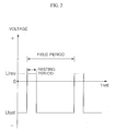
- FIG. 2 illustrates a pulsed DC bias voltage applied to a bias electrode
- FIG. 3 illustrates an apparatus for generating remote plasma according to another embodiment of the present invention.
- FIG. 1 is a sectional view illustrating an apparatus for generating remote plasma according to an embodiment of the present invention.
- a chamber 100 includes a plasma generating unit 250 and a reacting unit 260, which are vertically partitioned.
- the chamber 100 includes a sidewall 102, an upper insulation member 130, and a plurality of sealing blocks 110 and 120 for connecting the sidewall 102 and the upper insulation member 130 and enhancing the assemblability.
- the insulation member 130 may include, for example, quartz.
- a header 150 including a plasma gas supply passage 152 and a supply passage 154 for supplying a source gas or a purge gas is mounted on the insulation member 130.
- the supply passage 154 extends to a shower head 150, which will be described later.
- the supply passage 154 may be formed such that it extends to the shower head 500 from a side of the chamber 100.
- a radio frequency (RF) power is supplied to an RF electrode 200 so as to generate plasma, and a plurality of through holes 210 through which a plasma gas supplied through the plasma gas supply passage 152 passes are disposed in the RF electrode 200.
- RF radio frequency
- an RF antenna may be installed on the insulation member 130 instead of the RF electrode 200.
- An example of the RF antenna is disclosed in the Korean Patent Publication No. 2007-82746 , in which two loop antenna elements where a power supply terminal is formed at one end and a ground terminal is formed at the other end are horizontally spaced apart at regular intervals and electrically connected to each other in parallel, the power supply terminal and ground terminal of each antenna are symmetrically positioned with respect to the center of the antenna element, and a horizontally-bended portion of one of the antenna elements is placed between the power supply terminal and the ground terminal of the other one of the antennal elements.
- a ground electrode 400 to be described later is not required and therefore the configuration may be changed.
- a plasma generating unit 250 is formed between the RF electrode 200 and the bias electrode 300.
- the plasma generated in the plasma generating unit 250 is supplied into the chamber 100 via the bias electrode 300 and the ground electrode 400.
- the bias electrode 300 is positioned under the plasma generating unit 250 to trap positive ions in the plasma generated in the plasma generating unit 250.
- a plurality of through holes 310 through which the plasma pass are uniformly formed over the entire surface of the bias electrode 300. That is, the plurality of through holes 310 are uniformly formed in the bias electrode 300, and resultantly the plasma can be uniformly supplied to a target such as a wafer.
- the bias electrode 300 may be made of a metal and its surface may be anodized so that it is possible to prevent the contamination caused by metal impurities. Also, according to another embodiment of the present invention, an arc phenomenon caused by charges accumulated on the surface of the bias electrode 300 can be prevented by coating the entire surface of the bias electrode 300 with an etch-resistant metal containing tungsten or titanium.
- Through holes 410 through which the plasma pass are formed in the ground electrode 400 installed under and apart from the bias electrode 300.
- the through holes 410 of the ground electrode 400 are formed such that they are aligned with the through holes 310 of the bias electrode 300.
- the ground electrode 400 may be omitted when the RF antenna is employed instead of the RF electrode 200.
- a plasma guide hole 510 and a source gas guide hole 512 are formed.
- the plasma guide hole 510 corresponds to the through hole 410 of the ground electrode 400.
- a source gas or purge gas supplied through the supply passage 154 passes through the source gas guide hole 512. That is, the source gas or purge gas supplied through the supply passage 154 is introduced into a confined space formed between the surface of the shower head 500 and the rear side of the ground electrode 400, and then discharged through the source gas guide hole 512.
- a spray nozzle 514 may be formed on one end of the source gas guide hole 512.
- a source supply unit which differs in configuration from the shower head 500 may be employed. That is, a ring type source supply unit having, for example, spray holes, may be applicable instead of the shower head 500.
- a pulsed DC bias of a second voltage level which has a first voltage level, is applied to the bias electrode 300.
- FIG. 2 illustrates a pulsed DC bias voltage applied to the bias electrode 300.
- a negative pulsed DC bias having a positive voltage level during a predetermined period periodically is applied, however, the present invention is not limited thereto. Therefore, a positive pulsed DC having a negative level during a predetermined period periodically may be applied to the bias electrode 300.
- the pulsed DC bias includes a negative pulse Uset having a negative voltage level during a predetermined period basically, and also includes a positive pulse Urev having a positive level during a resting period.
- positive ions in the plasma are trapped on the surface of the bias electrode 300 due to the negative pulse Uset, and then the trapped positive ions are repelled toward the plasma generating unit 250 and vanished due to the positive pulse Urev. Otherwise, the trapped positive ions are neutralized by negative ions pulled by the positive pulse Urev.
- the present invention is advantageous in that it is possible to remove charges remaining on the bias electrode 300 because the bias electrode 300 is made of a metal, the metal impurity-caused contamination can be prevented by anodizing the surface of the bias electrode 300 during the generation of plasma, and the electrode itself acts as a capacitor.
- anodized surface is an insulator
- charges may be accumulated on the anodized surface, which may cause an arc to be generated.
- the entire surface of the bias electrode 300 may be coated with an etch-resistant metal containing tungsten or titanium according to another embodiment of the present invention. According to this embodiment, it is advantageous in that the bias electrode 300 can sufficiently stand up even if a small-scaled arc discharge is generated due to the charges remaining on the surface of the electrode 300 in spite of an applied pulsed DC bias.
- the charges remaining on the bias electrode 300 can be removed by connecting a capacitor to a bias power source in series. That is, the charges remaining on the bias electrode 300 can be removed because the charges remaining on the bias electrode 300 move toward one side electrode of the capacitor according to the electrostatic induction phenomenon and arranged to face charges of the other electrode of the capacitor.
- the apparatus for generating plasma according to the present invention is also applicable to a chemical vapor deposition (CVD) apparatus or an atomic layer deposition (ALD) where ON/OFF operations of plasma are frequently performed.
- the apparatus for generating plasma according to the present invention can be used to form an oxide, a silicon compound, a single crystal compound, a polycrystal compound, and an amorphous compound on a substrate of Si, SiGe, Ge, Al 2 O 3 , GaAs and SiC.
- a plasma source applied to the apparatus for generating plasma according to the present invention may include every plasma source, for example, high density plasma (HDP), inductively coupled plasma (ICP), capacitively coupled plasma (CCP), and electron cyclotron resonance (ECR).
- HDP high density plasma
- ICP inductively coupled plasma
- CCP capacitively coupled plasma
- ECR electron cyclotron resonance
- FIG. 3 illustrates an apparatus for generating remote plasma according to another embodiment of the present invention.
- FIG. 3 exemplarily illustrates an ICP generating apparatus in which a plasma generating unit 25 is formed over a chamber 40, and an ICP coil winds around the plasma generating unit 25. Furthermore, a header 10 having a plasma gas supply passage 12 is mounted on the plasma generating unit 25, and a supply pipe (not shown) is connected to an inlet of the plasma gas supply passage 12.
- a bias electrode 30 including a plurality of through holes 31 arranged regularly is installed between the plasma generating unit 25 and the chamber 40, and a substrate is loaded onto a substrate loading unit 60 inside the chamber 40.
- a negative pulsed DC bias having a positive voltage level periodically is also applied to the bias electrode 30 in this embodiment of FIG. 3 .
- a source supply unit 50 is disposed over the substrate loading unit 60.
- a ring type source supply unit 50 may be used, in which a plurality of spray holes through which a source gas or purge gas is sprayed are formed in the bottom surface.
- positive ions in the plasma are trapped on the surface of the bias electrode 300 due to the negative pulse Uset, and then the trapped positive ions are repelled toward the plasma generating unit 250 and vanished due to the positive pulse Urev. Otherwise, the trapped positive ions are neutralized by negative ions pulled by the positive pulse Urev.
- the source gas and purge gas may be supplied using a ring type source supply unit instead of a shower head.
- the positive ions created during the generation of plasma can be reliably trapped by applying a negative pulsed DC bias to a bias electrode, thus preventing a substrate and a thin film from being damaged and improving thin-film quality.
- the entire surface of the bias electrode is coated with an etch-resistant metal containing tungsten or titanium, and resultantly it is advantageous in that the bias electrode can sufficiently stand up even if a small-scaled arc discharge is generated due to residual charges.
- charges remaining on the bias electrode can be removed by connecting a capacitor to a pulsed DC bias power source in series.
Landscapes
- Physics & Mathematics (AREA)
- Engineering & Computer Science (AREA)
- Plasma & Fusion (AREA)
- Chemical & Material Sciences (AREA)
- Analytical Chemistry (AREA)
- Plasma Technology (AREA)
- Electron Sources, Ion Sources (AREA)
- Chemical Vapour Deposition (AREA)
Applications Claiming Priority (2)
| Application Number | Priority Date | Filing Date | Title |
|---|---|---|---|
| KR20080102578 | 2008-10-20 | ||
| KR1020090071296A KR101105907B1 (ko) | 2008-10-20 | 2009-08-03 | 리모트 플라즈마 발생장치 |
Publications (3)
| Publication Number | Publication Date |
|---|---|
| EP2178106A2 true EP2178106A2 (de) | 2010-04-21 |
| EP2178106A3 EP2178106A3 (de) | 2011-04-13 |
| EP2178106B1 EP2178106B1 (de) | 2016-03-02 |
Family
ID=41151765
Family Applications (1)
| Application Number | Title | Priority Date | Filing Date |
|---|---|---|---|
| EP09011022.2A Active EP2178106B1 (de) | 2008-10-20 | 2009-08-27 | Vorrichtung zur Erzeugung eines entfernten Plasmas |
Country Status (2)
| Country | Link |
|---|---|
| US (1) | US8207470B2 (de) |
| EP (1) | EP2178106B1 (de) |
Families Citing this family (105)
| Publication number | Priority date | Publication date | Assignee | Title |
|---|---|---|---|---|
| US9324576B2 (en) | 2010-05-27 | 2016-04-26 | Applied Materials, Inc. | Selective etch for silicon films |
| US10283321B2 (en) * | 2011-01-18 | 2019-05-07 | Applied Materials, Inc. | Semiconductor processing system and methods using capacitively coupled plasma |
| US8999856B2 (en) | 2011-03-14 | 2015-04-07 | Applied Materials, Inc. | Methods for etch of sin films |
| US9064815B2 (en) | 2011-03-14 | 2015-06-23 | Applied Materials, Inc. | Methods for etch of metal and metal-oxide films |
| US9267739B2 (en) | 2012-07-18 | 2016-02-23 | Applied Materials, Inc. | Pedestal with multi-zone temperature control and multiple purge capabilities |
| FR2993576B1 (fr) * | 2012-07-20 | 2018-05-18 | Nanoplas | Dispositif de traitement d'un objet par plasma |
| US9373517B2 (en) | 2012-08-02 | 2016-06-21 | Applied Materials, Inc. | Semiconductor processing with DC assisted RF power for improved control |
| TWI467625B (zh) * | 2012-08-30 | 2015-01-01 | 長庚大學 | 電漿處理裝置 |
| US9132436B2 (en) | 2012-09-21 | 2015-09-15 | Applied Materials, Inc. | Chemical control features in wafer process equipment |
| US10256079B2 (en) * | 2013-02-08 | 2019-04-09 | Applied Materials, Inc. | Semiconductor processing systems having multiple plasma configurations |
| US9362130B2 (en) | 2013-03-01 | 2016-06-07 | Applied Materials, Inc. | Enhanced etching processes using remote plasma sources |
| US20140271097A1 (en) | 2013-03-15 | 2014-09-18 | Applied Materials, Inc. | Processing systems and methods for halide scavenging |
| US9773648B2 (en) | 2013-08-30 | 2017-09-26 | Applied Materials, Inc. | Dual discharge modes operation for remote plasma |
| US9576809B2 (en) | 2013-11-04 | 2017-02-21 | Applied Materials, Inc. | Etch suppression with germanium |
| US9520303B2 (en) | 2013-11-12 | 2016-12-13 | Applied Materials, Inc. | Aluminum selective etch |
| US9133546B1 (en) | 2014-03-05 | 2015-09-15 | Lotus Applied Technology, Llc | Electrically- and chemically-active adlayers for plasma electrodes |
| US9299537B2 (en) | 2014-03-20 | 2016-03-29 | Applied Materials, Inc. | Radial waveguide systems and methods for post-match control of microwaves |
| US9903020B2 (en) | 2014-03-31 | 2018-02-27 | Applied Materials, Inc. | Generation of compact alumina passivation layers on aluminum plasma equipment components |
| KR102222902B1 (ko) | 2014-05-12 | 2021-03-05 | 삼성전자주식회사 | 플라즈마 장비 및 이를 이용한 반도체 소자의 제조 방법 |
| KR102386812B1 (ko) * | 2014-05-16 | 2022-04-15 | 어플라이드 머티어리얼스, 인코포레이티드 | 샤워헤드 설계 |
| US9309598B2 (en) | 2014-05-28 | 2016-04-12 | Applied Materials, Inc. | Oxide and metal removal |
| US20150348755A1 (en) * | 2014-05-29 | 2015-12-03 | Charm Engineering Co., Ltd. | Gas distribution apparatus and substrate processing apparatus including same |
| US9496167B2 (en) | 2014-07-31 | 2016-11-15 | Applied Materials, Inc. | Integrated bit-line airgap formation and gate stack post clean |
| US9659753B2 (en) | 2014-08-07 | 2017-05-23 | Applied Materials, Inc. | Grooved insulator to reduce leakage current |
| US9613822B2 (en) | 2014-09-25 | 2017-04-04 | Applied Materials, Inc. | Oxide etch selectivity enhancement |
| US9355922B2 (en) | 2014-10-14 | 2016-05-31 | Applied Materials, Inc. | Systems and methods for internal surface conditioning in plasma processing equipment |
| US9966240B2 (en) | 2014-10-14 | 2018-05-08 | Applied Materials, Inc. | Systems and methods for internal surface conditioning assessment in plasma processing equipment |
| US11637002B2 (en) | 2014-11-26 | 2023-04-25 | Applied Materials, Inc. | Methods and systems to enhance process uniformity |
| US10224210B2 (en) | 2014-12-09 | 2019-03-05 | Applied Materials, Inc. | Plasma processing system with direct outlet toroidal plasma source |
| US10573496B2 (en) | 2014-12-09 | 2020-02-25 | Applied Materials, Inc. | Direct outlet toroidal plasma source |
| US11257693B2 (en) | 2015-01-09 | 2022-02-22 | Applied Materials, Inc. | Methods and systems to improve pedestal temperature control |
| US9728437B2 (en) | 2015-02-03 | 2017-08-08 | Applied Materials, Inc. | High temperature chuck for plasma processing systems |
| US20160225652A1 (en) | 2015-02-03 | 2016-08-04 | Applied Materials, Inc. | Low temperature chuck for plasma processing systems |
| US9881805B2 (en) | 2015-03-02 | 2018-01-30 | Applied Materials, Inc. | Silicon selective removal |
| US9741593B2 (en) | 2015-08-06 | 2017-08-22 | Applied Materials, Inc. | Thermal management systems and methods for wafer processing systems |
| US9691645B2 (en) | 2015-08-06 | 2017-06-27 | Applied Materials, Inc. | Bolted wafer chuck thermal management systems and methods for wafer processing systems |
| US9349605B1 (en) | 2015-08-07 | 2016-05-24 | Applied Materials, Inc. | Oxide etch selectivity systems and methods |
| US10504700B2 (en) | 2015-08-27 | 2019-12-10 | Applied Materials, Inc. | Plasma etching systems and methods with secondary plasma injection |
| US10504754B2 (en) | 2016-05-19 | 2019-12-10 | Applied Materials, Inc. | Systems and methods for improved semiconductor etching and component protection |
| US10522371B2 (en) | 2016-05-19 | 2019-12-31 | Applied Materials, Inc. | Systems and methods for improved semiconductor etching and component protection |
| US9865484B1 (en) | 2016-06-29 | 2018-01-09 | Applied Materials, Inc. | Selective etch using material modification and RF pulsing |
| US10062575B2 (en) | 2016-09-09 | 2018-08-28 | Applied Materials, Inc. | Poly directional etch by oxidation |
| US10629473B2 (en) | 2016-09-09 | 2020-04-21 | Applied Materials, Inc. | Footing removal for nitride spacer |
| US10546729B2 (en) | 2016-10-04 | 2020-01-28 | Applied Materials, Inc. | Dual-channel showerhead with improved profile |
| US9934942B1 (en) | 2016-10-04 | 2018-04-03 | Applied Materials, Inc. | Chamber with flow-through source |
| US10062585B2 (en) | 2016-10-04 | 2018-08-28 | Applied Materials, Inc. | Oxygen compatible plasma source |
| US9721789B1 (en) | 2016-10-04 | 2017-08-01 | Applied Materials, Inc. | Saving ion-damaged spacers |
| US10062579B2 (en) | 2016-10-07 | 2018-08-28 | Applied Materials, Inc. | Selective SiN lateral recess |
| US9947549B1 (en) | 2016-10-10 | 2018-04-17 | Applied Materials, Inc. | Cobalt-containing material removal |
| US10163696B2 (en) | 2016-11-11 | 2018-12-25 | Applied Materials, Inc. | Selective cobalt removal for bottom up gapfill |
| US9768034B1 (en) | 2016-11-11 | 2017-09-19 | Applied Materials, Inc. | Removal methods for high aspect ratio structures |
| US10026621B2 (en) | 2016-11-14 | 2018-07-17 | Applied Materials, Inc. | SiN spacer profile patterning |
| US10242908B2 (en) | 2016-11-14 | 2019-03-26 | Applied Materials, Inc. | Airgap formation with damage-free copper |
| US10566206B2 (en) | 2016-12-27 | 2020-02-18 | Applied Materials, Inc. | Systems and methods for anisotropic material breakthrough |
| US10403507B2 (en) | 2017-02-03 | 2019-09-03 | Applied Materials, Inc. | Shaped etch profile with oxidation |
| US10431429B2 (en) | 2017-02-03 | 2019-10-01 | Applied Materials, Inc. | Systems and methods for radial and azimuthal control of plasma uniformity |
| US10043684B1 (en) | 2017-02-06 | 2018-08-07 | Applied Materials, Inc. | Self-limiting atomic thermal etching systems and methods |
| US10319739B2 (en) | 2017-02-08 | 2019-06-11 | Applied Materials, Inc. | Accommodating imperfectly aligned memory holes |
| US20180230597A1 (en) * | 2017-02-14 | 2018-08-16 | Applied Materials, Inc. | Method and apparatus of remote plasmas flowable cvd chamber |
| US10943834B2 (en) | 2017-03-13 | 2021-03-09 | Applied Materials, Inc. | Replacement contact process |
| US10319649B2 (en) | 2017-04-11 | 2019-06-11 | Applied Materials, Inc. | Optical emission spectroscopy (OES) for remote plasma monitoring |
| JP7176860B6 (ja) | 2017-05-17 | 2022-12-16 | アプライド マテリアルズ インコーポレイテッド | 前駆体の流れを改善する半導体処理チャンバ |
| US11276590B2 (en) | 2017-05-17 | 2022-03-15 | Applied Materials, Inc. | Multi-zone semiconductor substrate supports |
| US11276559B2 (en) | 2017-05-17 | 2022-03-15 | Applied Materials, Inc. | Semiconductor processing chamber for multiple precursor flow |
| US10497579B2 (en) | 2017-05-31 | 2019-12-03 | Applied Materials, Inc. | Water-free etching methods |
| US10049891B1 (en) | 2017-05-31 | 2018-08-14 | Applied Materials, Inc. | Selective in situ cobalt residue removal |
| US10920320B2 (en) | 2017-06-16 | 2021-02-16 | Applied Materials, Inc. | Plasma health determination in semiconductor substrate processing reactors |
| US10541246B2 (en) | 2017-06-26 | 2020-01-21 | Applied Materials, Inc. | 3D flash memory cells which discourage cross-cell electrical tunneling |
| US10727080B2 (en) | 2017-07-07 | 2020-07-28 | Applied Materials, Inc. | Tantalum-containing material removal |
| US10541184B2 (en) | 2017-07-11 | 2020-01-21 | Applied Materials, Inc. | Optical emission spectroscopic techniques for monitoring etching |
| KR102431354B1 (ko) | 2017-07-11 | 2022-08-11 | 삼성디스플레이 주식회사 | 화학기상 증착장치 및 이를 이용한 표시 장치의 제조 방법 |
| US10354889B2 (en) | 2017-07-17 | 2019-07-16 | Applied Materials, Inc. | Non-halogen etching of silicon-containing materials |
| US10043674B1 (en) | 2017-08-04 | 2018-08-07 | Applied Materials, Inc. | Germanium etching systems and methods |
| US10170336B1 (en) | 2017-08-04 | 2019-01-01 | Applied Materials, Inc. | Methods for anisotropic control of selective silicon removal |
| US10297458B2 (en) | 2017-08-07 | 2019-05-21 | Applied Materials, Inc. | Process window widening using coated parts in plasma etch processes |
| US10283324B1 (en) | 2017-10-24 | 2019-05-07 | Applied Materials, Inc. | Oxygen treatment for nitride etching |
| US10128086B1 (en) | 2017-10-24 | 2018-11-13 | Applied Materials, Inc. | Silicon pretreatment for nitride removal |
| US10256112B1 (en) | 2017-12-08 | 2019-04-09 | Applied Materials, Inc. | Selective tungsten removal |
| US10903054B2 (en) | 2017-12-19 | 2021-01-26 | Applied Materials, Inc. | Multi-zone gas distribution systems and methods |
| US11328909B2 (en) | 2017-12-22 | 2022-05-10 | Applied Materials, Inc. | Chamber conditioning and removal processes |
| US10854426B2 (en) | 2018-01-08 | 2020-12-01 | Applied Materials, Inc. | Metal recess for semiconductor structures |
| US10964512B2 (en) | 2018-02-15 | 2021-03-30 | Applied Materials, Inc. | Semiconductor processing chamber multistage mixing apparatus and methods |
| US10679870B2 (en) | 2018-02-15 | 2020-06-09 | Applied Materials, Inc. | Semiconductor processing chamber multistage mixing apparatus |
| TWI716818B (zh) | 2018-02-28 | 2021-01-21 | 美商應用材料股份有限公司 | 形成氣隙的系統及方法 |
| US10593560B2 (en) | 2018-03-01 | 2020-03-17 | Applied Materials, Inc. | Magnetic induction plasma source for semiconductor processes and equipment |
| US10319600B1 (en) | 2018-03-12 | 2019-06-11 | Applied Materials, Inc. | Thermal silicon etch |
| US10497573B2 (en) | 2018-03-13 | 2019-12-03 | Applied Materials, Inc. | Selective atomic layer etching of semiconductor materials |
| US10573527B2 (en) | 2018-04-06 | 2020-02-25 | Applied Materials, Inc. | Gas-phase selective etching systems and methods |
| US10490406B2 (en) | 2018-04-10 | 2019-11-26 | Appled Materials, Inc. | Systems and methods for material breakthrough |
| US10699879B2 (en) | 2018-04-17 | 2020-06-30 | Applied Materials, Inc. | Two piece electrode assembly with gap for plasma control |
| US10886137B2 (en) | 2018-04-30 | 2021-01-05 | Applied Materials, Inc. | Selective nitride removal |
| US10872778B2 (en) | 2018-07-06 | 2020-12-22 | Applied Materials, Inc. | Systems and methods utilizing solid-phase etchants |
| US10755941B2 (en) | 2018-07-06 | 2020-08-25 | Applied Materials, Inc. | Self-limiting selective etching systems and methods |
| US10672642B2 (en) | 2018-07-24 | 2020-06-02 | Applied Materials, Inc. | Systems and methods for pedestal configuration |
| US11049755B2 (en) | 2018-09-14 | 2021-06-29 | Applied Materials, Inc. | Semiconductor substrate supports with embedded RF shield |
| US10892198B2 (en) | 2018-09-14 | 2021-01-12 | Applied Materials, Inc. | Systems and methods for improved performance in semiconductor processing |
| US11062887B2 (en) | 2018-09-17 | 2021-07-13 | Applied Materials, Inc. | High temperature RF heater pedestals |
| US11417534B2 (en) | 2018-09-21 | 2022-08-16 | Applied Materials, Inc. | Selective material removal |
| US11682560B2 (en) | 2018-10-11 | 2023-06-20 | Applied Materials, Inc. | Systems and methods for hafnium-containing film removal |
| US11121002B2 (en) | 2018-10-24 | 2021-09-14 | Applied Materials, Inc. | Systems and methods for etching metals and metal derivatives |
| US11437242B2 (en) | 2018-11-27 | 2022-09-06 | Applied Materials, Inc. | Selective removal of silicon-containing materials |
| US11721527B2 (en) | 2019-01-07 | 2023-08-08 | Applied Materials, Inc. | Processing chamber mixing systems |
| US10920319B2 (en) | 2019-01-11 | 2021-02-16 | Applied Materials, Inc. | Ceramic showerheads with conductive electrodes |
| JP7443516B2 (ja) | 2020-06-01 | 2024-03-05 | 東京エレクトロン株式会社 | プラズマ処理装置及びプラズマ処理方法 |
| US20250006465A1 (en) * | 2023-06-27 | 2025-01-02 | Applied Materials, Inc. | Remote Plasma Source and Plasma Processing Chamber Having Same |
Citations (1)
| Publication number | Priority date | Publication date | Assignee | Title |
|---|---|---|---|---|
| KR20070082746A (ko) | 2006-02-17 | 2007-08-22 | 한양대학교 산학협력단 | 원거리 플라즈마 발생장치 |
Family Cites Families (7)
| Publication number | Priority date | Publication date | Assignee | Title |
|---|---|---|---|---|
| US4996077A (en) * | 1988-10-07 | 1991-02-26 | Texas Instruments Incorporated | Distributed ECR remote plasma processing and apparatus |
| US5614055A (en) * | 1993-08-27 | 1997-03-25 | Applied Materials, Inc. | High density plasma CVD and etching reactor |
| US5767683A (en) * | 1996-07-26 | 1998-06-16 | Stearns; Stanley D. | System for detecting compounds in a gaseous sample using photoionization, electron capture detection, and a constant current feedback control circuit which responds to compound concentration |
| JP4042817B2 (ja) * | 2001-03-26 | 2008-02-06 | 株式会社荏原製作所 | 中性粒子ビーム処理装置 |
| US7561208B2 (en) | 2003-06-23 | 2009-07-14 | Nxp B.V. | Method and decoder for composing a scene |
| US7767561B2 (en) * | 2004-07-20 | 2010-08-03 | Applied Materials, Inc. | Plasma immersion ion implantation reactor having an ion shower grid |
| US20090302002A1 (en) * | 2008-02-29 | 2009-12-10 | Applied Materials, Inc. | Method and apparatus for removing polymer from a substrate |
-
2009
- 2009-08-25 US US12/547,163 patent/US8207470B2/en active Active
- 2009-08-27 EP EP09011022.2A patent/EP2178106B1/de active Active
Patent Citations (1)
| Publication number | Priority date | Publication date | Assignee | Title |
|---|---|---|---|---|
| KR20070082746A (ko) | 2006-02-17 | 2007-08-22 | 한양대학교 산학협력단 | 원거리 플라즈마 발생장치 |
Also Published As
| Publication number | Publication date |
|---|---|
| US8207470B2 (en) | 2012-06-26 |
| EP2178106A3 (de) | 2011-04-13 |
| EP2178106B1 (de) | 2016-03-02 |
| US20100096367A1 (en) | 2010-04-22 |
Similar Documents
| Publication | Publication Date | Title |
|---|---|---|
| US8207470B2 (en) | Apparatus for generating remote plasma | |
| EP2026374B1 (de) | Plasmaverarbeitungsvorrichtung, Plasmaverarbeitungsverfahren und Speichermedium | |
| KR101526020B1 (ko) | 플라즈마 프로세싱 챔버 및 이의 내에서 기판의 베벨 에지 및 챔버 내부를 세정하는 방법 | |
| KR100752622B1 (ko) | 원거리 플라즈마 발생장치 | |
| KR102827035B1 (ko) | 펄스식 플라즈마를 사용하여 에칭 선택도를 향상시키는 방법 | |
| US20120052689A1 (en) | Plasma etching method and apparatus thereof | |
| US12400845B2 (en) | Ion energy control on electrodes in a plasma reactor | |
| EP1840937A1 (de) | Gerät und Verfahren zur Plasmabehandlung | |
| US20060102286A1 (en) | Plasma processing apparatus | |
| KR20240012556A (ko) | 플라즈마 챔버 및 챔버 컴포넌트 세정 방법들 | |
| CN101198207B (zh) | 等离子体处理设备 | |
| US8906471B2 (en) | Method of depositing metallic film by plasma CVD and storage medium | |
| CN117751421A (zh) | 用于对等离子体中的离子能量分布进行数字控制的方法和装置 | |
| US8277906B2 (en) | Method of processing a substrate | |
| US20170186591A1 (en) | Cleaning method of plasma processing apparatus and plasma processing apparatus | |
| CN107680896A (zh) | 基板处理装置以及基板处理方法 | |
| KR101105907B1 (ko) | 리모트 플라즈마 발생장치 | |
| US12448680B2 (en) | Method of forming pattern structure including silicon nitride | |
| US20170087602A1 (en) | Method and apparatus for treating substrate | |
| KR20160003624A (ko) | 에칭 방법 | |
| KR20100006715U (ko) | 화학 기상 증착 장치의 펌핑 플레이트 | |
| KR20090086783A (ko) | 플라즈마 식각 장치 | |
| KR100798416B1 (ko) | 플라즈마 처리장치 | |
| US20230282452A1 (en) | Cleaning method, method of manufacturing semiconductor device, plasma treatment device, and outer circumferential ring set | |
| KR100725614B1 (ko) | 플라즈마 처리 장치 |
Legal Events
| Date | Code | Title | Description |
|---|---|---|---|
| PUAI | Public reference made under article 153(3) epc to a published international application that has entered the european phase |
Free format text: ORIGINAL CODE: 0009012 |
|
| 17P | Request for examination filed |
Effective date: 20090827 |
|
| AK | Designated contracting states |
Kind code of ref document: A2 Designated state(s): AT BE BG CH CY CZ DE DK EE ES FI FR GB GR HR HU IE IS IT LI LT LU LV MC MK MT NL NO PL PT RO SE SI SK SM TR |
|
| AX | Request for extension of the european patent |
Extension state: AL BA RS |
|
| PUAL | Search report despatched |
Free format text: ORIGINAL CODE: 0009013 |
|
| AK | Designated contracting states |
Kind code of ref document: A3 Designated state(s): AT BE BG CH CY CZ DE DK EE ES FI FR GB GR HR HU IE IS IT LI LT LU LV MC MK MT NL NO PL PT RO SE SI SK SM TR |
|
| AX | Request for extension of the european patent |
Extension state: AL BA RS |
|
| 17Q | First examination report despatched |
Effective date: 20131106 |
|
| GRAP | Despatch of communication of intention to grant a patent |
Free format text: ORIGINAL CODE: EPIDOSNIGR1 |
|
| INTG | Intention to grant announced |
Effective date: 20150929 |
|
| GRAS | Grant fee paid |
Free format text: ORIGINAL CODE: EPIDOSNIGR3 |
|
| GRAA | (expected) grant |
Free format text: ORIGINAL CODE: 0009210 |
|
| AK | Designated contracting states |
Kind code of ref document: B1 Designated state(s): AT BE BG CH CY CZ DE DK EE ES FI FR GB GR HR HU IE IS IT LI LT LU LV MC MK MT NL NO PL PT RO SE SI SK SM TR |
|
| REG | Reference to a national code |
Ref country code: GB Ref legal event code: FG4D |
|
| REG | Reference to a national code |
Ref country code: AT Ref legal event code: REF Ref document number: 778532 Country of ref document: AT Kind code of ref document: T Effective date: 20160315 Ref country code: CH Ref legal event code: EP |
|
| REG | Reference to a national code |
Ref country code: IE Ref legal event code: FG4D |
|
| REG | Reference to a national code |
Ref country code: DE Ref legal event code: R096 Ref document number: 602009036561 Country of ref document: DE |
|
| REG | Reference to a national code |
Ref country code: NL Ref legal event code: FP |
|
| REG | Reference to a national code |
Ref country code: LT Ref legal event code: MG4D |
|
| REG | Reference to a national code |
Ref country code: AT Ref legal event code: MK05 Ref document number: 778532 Country of ref document: AT Kind code of ref document: T Effective date: 20160302 |
|
| PG25 | Lapsed in a contracting state [announced via postgrant information from national office to epo] |
Ref country code: GR Free format text: LAPSE BECAUSE OF FAILURE TO SUBMIT A TRANSLATION OF THE DESCRIPTION OR TO PAY THE FEE WITHIN THE PRESCRIBED TIME-LIMIT Effective date: 20160603 Ref country code: HR Free format text: LAPSE BECAUSE OF FAILURE TO SUBMIT A TRANSLATION OF THE DESCRIPTION OR TO PAY THE FEE WITHIN THE PRESCRIBED TIME-LIMIT Effective date: 20160302 Ref country code: NO Free format text: LAPSE BECAUSE OF FAILURE TO SUBMIT A TRANSLATION OF THE DESCRIPTION OR TO PAY THE FEE WITHIN THE PRESCRIBED TIME-LIMIT Effective date: 20160602 Ref country code: ES Free format text: LAPSE BECAUSE OF FAILURE TO SUBMIT A TRANSLATION OF THE DESCRIPTION OR TO PAY THE FEE WITHIN THE PRESCRIBED TIME-LIMIT Effective date: 20160302 Ref country code: FI Free format text: LAPSE BECAUSE OF FAILURE TO SUBMIT A TRANSLATION OF THE DESCRIPTION OR TO PAY THE FEE WITHIN THE PRESCRIBED TIME-LIMIT Effective date: 20160302 |
|
| REG | Reference to a national code |
Ref country code: FR Ref legal event code: PLFP Year of fee payment: 8 |
|
| PG25 | Lapsed in a contracting state [announced via postgrant information from national office to epo] |
Ref country code: LV Free format text: LAPSE BECAUSE OF FAILURE TO SUBMIT A TRANSLATION OF THE DESCRIPTION OR TO PAY THE FEE WITHIN THE PRESCRIBED TIME-LIMIT Effective date: 20160302 Ref country code: AT Free format text: LAPSE BECAUSE OF FAILURE TO SUBMIT A TRANSLATION OF THE DESCRIPTION OR TO PAY THE FEE WITHIN THE PRESCRIBED TIME-LIMIT Effective date: 20160302 Ref country code: LT Free format text: LAPSE BECAUSE OF FAILURE TO SUBMIT A TRANSLATION OF THE DESCRIPTION OR TO PAY THE FEE WITHIN THE PRESCRIBED TIME-LIMIT Effective date: 20160302 Ref country code: SE Free format text: LAPSE BECAUSE OF FAILURE TO SUBMIT A TRANSLATION OF THE DESCRIPTION OR TO PAY THE FEE WITHIN THE PRESCRIBED TIME-LIMIT Effective date: 20160302 Ref country code: PL Free format text: LAPSE BECAUSE OF FAILURE TO SUBMIT A TRANSLATION OF THE DESCRIPTION OR TO PAY THE FEE WITHIN THE PRESCRIBED TIME-LIMIT Effective date: 20160302 |
|
| PG25 | Lapsed in a contracting state [announced via postgrant information from national office to epo] |
Ref country code: EE Free format text: LAPSE BECAUSE OF FAILURE TO SUBMIT A TRANSLATION OF THE DESCRIPTION OR TO PAY THE FEE WITHIN THE PRESCRIBED TIME-LIMIT Effective date: 20160302 Ref country code: IS Free format text: LAPSE BECAUSE OF FAILURE TO SUBMIT A TRANSLATION OF THE DESCRIPTION OR TO PAY THE FEE WITHIN THE PRESCRIBED TIME-LIMIT Effective date: 20160702 |
|
| PG25 | Lapsed in a contracting state [announced via postgrant information from national office to epo] |
Ref country code: RO Free format text: LAPSE BECAUSE OF FAILURE TO SUBMIT A TRANSLATION OF THE DESCRIPTION OR TO PAY THE FEE WITHIN THE PRESCRIBED TIME-LIMIT Effective date: 20160302 Ref country code: PT Free format text: LAPSE BECAUSE OF FAILURE TO SUBMIT A TRANSLATION OF THE DESCRIPTION OR TO PAY THE FEE WITHIN THE PRESCRIBED TIME-LIMIT Effective date: 20160704 Ref country code: CZ Free format text: LAPSE BECAUSE OF FAILURE TO SUBMIT A TRANSLATION OF THE DESCRIPTION OR TO PAY THE FEE WITHIN THE PRESCRIBED TIME-LIMIT Effective date: 20160302 Ref country code: SM Free format text: LAPSE BECAUSE OF FAILURE TO SUBMIT A TRANSLATION OF THE DESCRIPTION OR TO PAY THE FEE WITHIN THE PRESCRIBED TIME-LIMIT Effective date: 20160302 Ref country code: SK Free format text: LAPSE BECAUSE OF FAILURE TO SUBMIT A TRANSLATION OF THE DESCRIPTION OR TO PAY THE FEE WITHIN THE PRESCRIBED TIME-LIMIT Effective date: 20160302 |
|
| REG | Reference to a national code |
Ref country code: DE Ref legal event code: R097 Ref document number: 602009036561 Country of ref document: DE |
|
| PG25 | Lapsed in a contracting state [announced via postgrant information from national office to epo] |
Ref country code: IT Free format text: LAPSE BECAUSE OF FAILURE TO SUBMIT A TRANSLATION OF THE DESCRIPTION OR TO PAY THE FEE WITHIN THE PRESCRIBED TIME-LIMIT Effective date: 20160302 Ref country code: BE Free format text: LAPSE BECAUSE OF FAILURE TO SUBMIT A TRANSLATION OF THE DESCRIPTION OR TO PAY THE FEE WITHIN THE PRESCRIBED TIME-LIMIT Effective date: 20160302 |
|
| PLBE | No opposition filed within time limit |
Free format text: ORIGINAL CODE: 0009261 |
|
| STAA | Information on the status of an ep patent application or granted ep patent |
Free format text: STATUS: NO OPPOSITION FILED WITHIN TIME LIMIT |
|
| PG25 | Lapsed in a contracting state [announced via postgrant information from national office to epo] |
Ref country code: DK Free format text: LAPSE BECAUSE OF FAILURE TO SUBMIT A TRANSLATION OF THE DESCRIPTION OR TO PAY THE FEE WITHIN THE PRESCRIBED TIME-LIMIT Effective date: 20160302 |
|
| 26N | No opposition filed |
Effective date: 20161205 |
|
| PG25 | Lapsed in a contracting state [announced via postgrant information from national office to epo] |
Ref country code: SI Free format text: LAPSE BECAUSE OF FAILURE TO SUBMIT A TRANSLATION OF THE DESCRIPTION OR TO PAY THE FEE WITHIN THE PRESCRIBED TIME-LIMIT Effective date: 20160302 Ref country code: BG Free format text: LAPSE BECAUSE OF FAILURE TO SUBMIT A TRANSLATION OF THE DESCRIPTION OR TO PAY THE FEE WITHIN THE PRESCRIBED TIME-LIMIT Effective date: 20160602 |
|
| PG25 | Lapsed in a contracting state [announced via postgrant information from national office to epo] |
Ref country code: MC Free format text: LAPSE BECAUSE OF FAILURE TO SUBMIT A TRANSLATION OF THE DESCRIPTION OR TO PAY THE FEE WITHIN THE PRESCRIBED TIME-LIMIT Effective date: 20160302 |
|
| REG | Reference to a national code |
Ref country code: CH Ref legal event code: PL |
|
| GBPC | Gb: european patent ceased through non-payment of renewal fee |
Effective date: 20160827 |
|
| PG25 | Lapsed in a contracting state [announced via postgrant information from national office to epo] |
Ref country code: LI Free format text: LAPSE BECAUSE OF NON-PAYMENT OF DUE FEES Effective date: 20160831 Ref country code: CH Free format text: LAPSE BECAUSE OF NON-PAYMENT OF DUE FEES Effective date: 20160831 |
|
| REG | Reference to a national code |
Ref country code: IE Ref legal event code: MM4A |
|
| REG | Reference to a national code |
Ref country code: FR Ref legal event code: PLFP Year of fee payment: 9 |
|
| PG25 | Lapsed in a contracting state [announced via postgrant information from national office to epo] |
Ref country code: GB Free format text: LAPSE BECAUSE OF NON-PAYMENT OF DUE FEES Effective date: 20160827 Ref country code: IE Free format text: LAPSE BECAUSE OF NON-PAYMENT OF DUE FEES Effective date: 20160827 |
|
| PG25 | Lapsed in a contracting state [announced via postgrant information from national office to epo] |
Ref country code: LU Free format text: LAPSE BECAUSE OF NON-PAYMENT OF DUE FEES Effective date: 20160827 |
|
| PG25 | Lapsed in a contracting state [announced via postgrant information from national office to epo] |
Ref country code: HU Free format text: LAPSE BECAUSE OF FAILURE TO SUBMIT A TRANSLATION OF THE DESCRIPTION OR TO PAY THE FEE WITHIN THE PRESCRIBED TIME-LIMIT; INVALID AB INITIO Effective date: 20090827 Ref country code: CY Free format text: LAPSE BECAUSE OF FAILURE TO SUBMIT A TRANSLATION OF THE DESCRIPTION OR TO PAY THE FEE WITHIN THE PRESCRIBED TIME-LIMIT Effective date: 20160302 |
|
| REG | Reference to a national code |
Ref country code: FR Ref legal event code: PLFP Year of fee payment: 10 |
|
| PG25 | Lapsed in a contracting state [announced via postgrant information from national office to epo] |
Ref country code: MT Free format text: LAPSE BECAUSE OF NON-PAYMENT OF DUE FEES Effective date: 20160831 Ref country code: MK Free format text: LAPSE BECAUSE OF FAILURE TO SUBMIT A TRANSLATION OF THE DESCRIPTION OR TO PAY THE FEE WITHIN THE PRESCRIBED TIME-LIMIT Effective date: 20160302 Ref country code: TR Free format text: LAPSE BECAUSE OF FAILURE TO SUBMIT A TRANSLATION OF THE DESCRIPTION OR TO PAY THE FEE WITHIN THE PRESCRIBED TIME-LIMIT Effective date: 20160302 |
|
| REG | Reference to a national code |
Ref country code: DE Ref legal event code: R081 Ref document number: 602009036561 Country of ref document: DE Owner name: TOKYO ELECTRON LTD., JP Free format text: FORMER OWNER: INDUSTRY-UNIVERSITY COOPERATION FOUNDATION HANYANG UNIVERSITY, SEOUL, KR |
|
| REG | Reference to a national code |
Ref country code: NL Ref legal event code: PD Owner name: TOKYO ELECTRON LTD.; JP Free format text: DETAILS ASSIGNMENT: CHANGE OF OWNER(S), ASSIGNMENT; FORMER OWNER NAME: INDUSTRY-UNIVERSITY COOPERATION FOUNDATION HANYANG UNIVERSITY Effective date: 20220328 |
|
| PGFP | Annual fee paid to national office [announced via postgrant information from national office to epo] |
Ref country code: NL Payment date: 20250704 Year of fee payment: 17 |
|
| PGFP | Annual fee paid to national office [announced via postgrant information from national office to epo] |
Ref country code: DE Payment date: 20250702 Year of fee payment: 17 |
|
| PGFP | Annual fee paid to national office [announced via postgrant information from national office to epo] |
Ref country code: FR Payment date: 20250703 Year of fee payment: 17 |