EP2178154B1 - Dispositif de ligne électrique - Google Patents
Dispositif de ligne électrique Download PDFInfo
- Publication number
- EP2178154B1 EP2178154B1 EP20090172550 EP09172550A EP2178154B1 EP 2178154 B1 EP2178154 B1 EP 2178154B1 EP 20090172550 EP20090172550 EP 20090172550 EP 09172550 A EP09172550 A EP 09172550A EP 2178154 B1 EP2178154 B1 EP 2178154B1
- Authority
- EP
- European Patent Office
- Prior art keywords
- conductors
- conductor
- arrangement according
- conduction arrangement
- separate
- Prior art date
- Legal status (The legal status is an assumption and is not a legal conclusion. Google has not performed a legal analysis and makes no representation as to the accuracy of the status listed.)
- Not-in-force
Links
- 239000004020 conductor Substances 0.000 claims description 157
- 239000000758 substrate Substances 0.000 claims description 28
- 230000005540 biological transmission Effects 0.000 claims description 9
- 238000006073 displacement reaction Methods 0.000 claims description 4
- 238000001746 injection moulding Methods 0.000 claims description 4
- 238000000034 method Methods 0.000 claims description 4
- 238000007765 extrusion coating Methods 0.000 claims 1
- 230000008878 coupling Effects 0.000 description 5
- 238000010168 coupling process Methods 0.000 description 5
- 238000005859 coupling reaction Methods 0.000 description 5
- 230000015572 biosynthetic process Effects 0.000 description 3
- 238000005755 formation reaction Methods 0.000 description 3
- 125000006850 spacer group Chemical group 0.000 description 3
- 238000005538 encapsulation Methods 0.000 description 2
- 230000036039 immunity Effects 0.000 description 2
- 230000001939 inductive effect Effects 0.000 description 2
- 238000004519 manufacturing process Methods 0.000 description 2
- 238000004080 punching Methods 0.000 description 2
- RYGMFSIKBFXOCR-UHFFFAOYSA-N Copper Chemical compound [Cu] RYGMFSIKBFXOCR-UHFFFAOYSA-N 0.000 description 1
- 150000001875 compounds Chemical class 0.000 description 1
- 238000010276 construction Methods 0.000 description 1
- 229910052802 copper Inorganic materials 0.000 description 1
- 239000010949 copper Substances 0.000 description 1
- 230000007423 decrease Effects 0.000 description 1
- 230000001419 dependent effect Effects 0.000 description 1
- 238000005516 engineering process Methods 0.000 description 1
- 239000000463 material Substances 0.000 description 1
- 238000003825 pressing Methods 0.000 description 1
- 238000005476 soldering Methods 0.000 description 1
- 230000001629 suppression Effects 0.000 description 1
- 238000003466 welding Methods 0.000 description 1
Images

Classifications
-
- H—ELECTRICITY
- H01—ELECTRIC ELEMENTS
- H01P—WAVEGUIDES; RESONATORS, LINES, OR OTHER DEVICES OF THE WAVEGUIDE TYPE
- H01P3/00—Waveguides; Transmission lines of the waveguide type
- H01P3/02—Waveguides; Transmission lines of the waveguide type with two longitudinal conductors
- H01P3/08—Microstrips; Strip lines
- H01P3/088—Stacked transmission lines
-
- H—ELECTRICITY
- H01—ELECTRIC ELEMENTS
- H01P—WAVEGUIDES; RESONATORS, LINES, OR OTHER DEVICES OF THE WAVEGUIDE TYPE
- H01P11/00—Apparatus or processes specially adapted for manufacturing waveguides or resonators, lines, or other devices of the waveguide type
- H01P11/001—Manufacturing waveguides or transmission lines of the waveguide type
-
- H—ELECTRICITY
- H01—ELECTRIC ELEMENTS
- H01P—WAVEGUIDES; RESONATORS, LINES, OR OTHER DEVICES OF THE WAVEGUIDE TYPE
- H01P3/00—Waveguides; Transmission lines of the waveguide type
- H01P3/02—Waveguides; Transmission lines of the waveguide type with two longitudinal conductors
- H01P3/026—Coplanar striplines [CPS]
-
- H—ELECTRICITY
- H05—ELECTRIC TECHNIQUES NOT OTHERWISE PROVIDED FOR
- H05K—PRINTED CIRCUITS; CASINGS OR CONSTRUCTIONAL DETAILS OF ELECTRIC APPARATUS; MANUFACTURE OF ASSEMBLAGES OF ELECTRICAL COMPONENTS
- H05K1/00—Printed circuits
- H05K1/02—Details
- H05K1/0213—Electrical arrangements not otherwise provided for
- H05K1/0216—Reduction of cross-talk, noise or electromagnetic interference
- H05K1/0228—Compensation of cross-talk by a mutually correlated lay-out of printed circuit traces, e.g. for compensation of cross-talk in mounted connectors
-
- H—ELECTRICITY
- H05—ELECTRIC TECHNIQUES NOT OTHERWISE PROVIDED FOR
- H05K—PRINTED CIRCUITS; CASINGS OR CONSTRUCTIONAL DETAILS OF ELECTRIC APPARATUS; MANUFACTURE OF ASSEMBLAGES OF ELECTRICAL COMPONENTS
- H05K1/00—Printed circuits
- H05K1/02—Details
- H05K1/0213—Electrical arrangements not otherwise provided for
- H05K1/0237—High frequency adaptations
-
- H—ELECTRICITY
- H05—ELECTRIC TECHNIQUES NOT OTHERWISE PROVIDED FOR
- H05K—PRINTED CIRCUITS; CASINGS OR CONSTRUCTIONAL DETAILS OF ELECTRIC APPARATUS; MANUFACTURE OF ASSEMBLAGES OF ELECTRICAL COMPONENTS
- H05K1/00—Printed circuits
- H05K1/02—Details
- H05K1/03—Use of materials for the substrate
- H05K1/0393—Flexible materials
-
- H—ELECTRICITY
- H05—ELECTRIC TECHNIQUES NOT OTHERWISE PROVIDED FOR
- H05K—PRINTED CIRCUITS; CASINGS OR CONSTRUCTIONAL DETAILS OF ELECTRIC APPARATUS; MANUFACTURE OF ASSEMBLAGES OF ELECTRICAL COMPONENTS
- H05K2201/00—Indexing scheme relating to printed circuits covered by H05K1/00
- H05K2201/05—Flexible printed circuits [FPCs]
- H05K2201/055—Folded back on itself
-
- H—ELECTRICITY
- H05—ELECTRIC TECHNIQUES NOT OTHERWISE PROVIDED FOR
- H05K—PRINTED CIRCUITS; CASINGS OR CONSTRUCTIONAL DETAILS OF ELECTRIC APPARATUS; MANUFACTURE OF ASSEMBLAGES OF ELECTRICAL COMPONENTS
- H05K2201/00—Indexing scheme relating to printed circuits covered by H05K1/00
- H05K2201/09—Shape and layout
- H05K2201/09009—Substrate related
- H05K2201/09118—Moulded substrate
-
- H—ELECTRICITY
- H05—ELECTRIC TECHNIQUES NOT OTHERWISE PROVIDED FOR
- H05K—PRINTED CIRCUITS; CASINGS OR CONSTRUCTIONAL DETAILS OF ELECTRIC APPARATUS; MANUFACTURE OF ASSEMBLAGES OF ELECTRICAL COMPONENTS
- H05K2201/00—Indexing scheme relating to printed circuits covered by H05K1/00
- H05K2201/09—Shape and layout
- H05K2201/09209—Shape and layout details of conductors
- H05K2201/09218—Conductive traces
- H05K2201/09236—Parallel layout
-
- H—ELECTRICITY
- H05—ELECTRIC TECHNIQUES NOT OTHERWISE PROVIDED FOR
- H05K—PRINTED CIRCUITS; CASINGS OR CONSTRUCTIONAL DETAILS OF ELECTRIC APPARATUS; MANUFACTURE OF ASSEMBLAGES OF ELECTRICAL COMPONENTS
- H05K2201/00—Indexing scheme relating to printed circuits covered by H05K1/00
- H05K2201/09—Shape and layout
- H05K2201/09209—Shape and layout details of conductors
- H05K2201/09218—Conductive traces
- H05K2201/09245—Crossing layout
-
- H—ELECTRICITY
- H05—ELECTRIC TECHNIQUES NOT OTHERWISE PROVIDED FOR
- H05K—PRINTED CIRCUITS; CASINGS OR CONSTRUCTIONAL DETAILS OF ELECTRIC APPARATUS; MANUFACTURE OF ASSEMBLAGES OF ELECTRICAL COMPONENTS
- H05K3/00—Apparatus or processes for manufacturing printed circuits
- H05K3/10—Apparatus or processes for manufacturing printed circuits in which conductive material is applied to the insulating support in such a manner as to form the desired conductive pattern
- H05K3/20—Apparatus or processes for manufacturing printed circuits in which conductive material is applied to the insulating support in such a manner as to form the desired conductive pattern by affixing prefabricated conductor pattern
- H05K3/202—Apparatus or processes for manufacturing printed circuits in which conductive material is applied to the insulating support in such a manner as to form the desired conductive pattern by affixing prefabricated conductor pattern using self-supporting metal foil pattern
Definitions
- the invention relates to an electrical, in particular a data transmission serving line arrangement with at least two substantially parallel electrical conductors.
- WO 2006/036689 A is an electrical, in particular serving for data transmission line arrangement is known, which has at least two, substantially parallel electrical conductor.
- the ladders cross at least one place.
- From the DE 197 38 754 A1 is a flexible, printed circuit with two electrically conductive wires, which are wave-shaped and are positioned one above the other so that they intersect in sections.
- the JP 2001-236479 A discloses a non-contact IC card having a flexible substrate on which a spiral antenna coil and tracks are formed, wherein a conductor member is folded to form a conductive bridge.
- Data transmissions of, for example, symmetrical signals are usually carried out in shielded and specially designed data cables. Their construction suppresses the emission of the useful signals via the inductive and capacitive coupling, and in the immunity to other interference fields, the inductive component is also suppressed, wherein the capacitive coupling leads to a common-mode voltage on the lines, which is suppressed with suitable input circuits. If such data signals, so in particular symmetrical signals such as CAN or Flexray over Led plug and / or punched grid structures or performed in parallel in another way, increases the interference emission of the useful signals on the coupling to other lines, the interference suppression of external interference decreases sharply.
- the object of the invention is to provide an electrical, in particular a data transmission serving line arrangement with at least two substantially parallel electrical conductors, which avoids the disadvantages mentioned and a very interference-proof data transmission with high interference immunity to external interference fields and with only a small emission of their own interference signals allows.
- an electrical, in particular a data transmission serving line arrangement is proposed with at least two substantially parallel electrical conductors. It is provided that the conductors have at least one crossover.
- two-dimensional electrical connections such as punched grids, printed circuit boards or flexible printed circuits
- the above-mentioned disadvantageous phenomena result from couplings of the two conductors to the environment.
- the crossover is in this case for maximum effectiveness at the electrical center of the parallel guidance of the two electrical conductors, ie in the middle of the parallel guidance of the two electrical conductors considered here. If, for example, they run parallel for a certain distance s (namely the electrical length), the center of the crossover is at maximum effectiveness at s / 2. If several crossovers are provided distributed over the electrical length, they are preferably evenly spaced and distributed.
- the crossover has at least one separate, electrically connected conductor element.
- the crossover is performed so that there is an interruption of one of the conductors in the case of an arrangement offset.
- the conductors are formed as conductor tracks. Under printed conductors are understood here in the broadest sense, all directly on a substrate overhead conductors, such as copper conductors on a circuit board.
- the conductors are formed on a flexible substrate.
- a flexible substrate for example, a film into consideration, on which the conductors are applied.
- the crossover is effected by an S-shaped configuration of the conductors and an overlapping of the conductors in the region of the S-shaped configuration, which takes place by folding of the substrate, at least in regions.
- This example is particularly advantageous in applying the conductors to a flexible substrate, as it is made possible by a corresponding arrangement of the conductors, as described in S-shaped design, and by simple folding of the flexible substrate. The folding does not have to bring about a juxtaposition of the substrate surfaces or substrate parts, but these can also be spaced; It is only essential that the S-shaped design of the conductor comes in corresponding counter-overlay to form the crossover (resulting, for example, as a projection through both, folded substrate surfaces).
- the conductors are formed as stamped grid tracks. Punching grids are used for the transmission of partially high currents, especially in automotive technology. In this case, it is preferably possible to also transmit data signals via such leadframe webs, wherein the transmission of data signals can be effected simultaneously to an operating voltage supply of electrical components of the vehicle. In particular, separate data lines can be saved in this way.
- the conductors are located on an electrically non-conductive conductor substrate.
- the conductors are therefore not completely insulated, but are in more or less uninsulated form on the conductor substrate, while being held by the conductor substrate and insulated from each other.
- one of the conductors for forming the crossover is guided in an S shape and the other conductor is guided straight to the crossover. From the crossover of the other conductor is again guided straight, with at least one separate conductor element, the two straight conductor pieces connected obliquely to each other, and this oblique, separate conductor element in the S-region of a conductor out, with a conductor but not electrically connected is.
- the crossing is thus carried out such that the one conductor is guided in an S-shape, while the other conductor is currently guided, but interrupted in the S-region of the one conductor.
- the S-shaped conductor is guided so that it is aligned after leaving its S-range with the interrupted, just guided other conductor.
- the two interrupted, just guided, other ladder are therefore once left, once right of the S-range.
- These two straight guided, other conductor pieces are conductively connected to each other by means of the separate conductor element, but the separate conductor element with the S-shaped guided a conductor is not electrically connected.
- the separate conductor element is held according to the invention by means of an electrically non-conductive support apparatus on at least one of the conductors.
- the support apparatus thus serves to hold the separate conductor element.
- the support apparatus is assigned to at least one of the conductors.
- the separate conductor element is electrically connected to the conductor pieces, in particular welded.
- other types of compound come into consideration, in particular those that can be easily and inexpensively produced and require only a short process time, such as riveting, pressing, soldering.
- the support apparatus has at least one transverse element, which is supported on the two conductors at a distance from the crossover, wherein from the transverse element emanates a boom to which the separate conductor element is attached.
- the support apparatus is thus supported on its cross member on the two conductors in such a way that the cross member is at a distance from the crossover. From this cross member goes out the boom to which the separate conductor element is attached.
- the separate conductor element is thus held by the cantilever.
- the boom in turn is held by the cross member, which is supported on the ladders or holds on this, for example by means of a clamp.
- Such a method of attachment is fast and inexpensive to produce.
- the support apparatus or at least a portion thereof in the plastic injection molding process, in particular in the plastic injection molding process created.
- the support apparatus is made of plastic very easy and inexpensive to produce. He may in this case have such a configuration in which it surrounds as a plastic component at least one, preferably both conductors, for example, applied by clamping and is thus supported on the conductors. It can also be made in such a way that it is sprayed around the conductors in the plastic injection molding process. As a result, a defined, predetermined arrangement of the conductors can already be achieved by encapsulation or partial encapsulation to form the support apparatus.
- the separate conductor element is formed integrally with one of the two conductor pieces being guided straight.
- This one conductor piece is thus formed in such a manner that the execution of the crossover results by superimposing the other conductor and the one conductor, wherein the conductors are spaced from each other.
- the support apparatus or a support or insulating element can be introduced in particular in the region of the crossover, preferably in such a manner that both conductors are supported on it in the area of the crossover.
- FIG. 1 shows an exemplary line arrangement 1 with two substantially parallel electrical conductors 2.
- the electrical conductors 2 are applied on one side of a substrate 3, which is formed as an electrically non-conductive conductor substrate 4 and 4 as a flexible substrate.
- Each of the two conductors 2 has an S-shaped configuration 6, wherein the two conductors 2 and the S-shaped formations 6 are aligned in a plane-parallel arrangement of the two conductors 2 on a flat, so not yet flattened or folded substrate 3, in the same direction.
- the two conductors 2 have in the plane-parallel, that is not folded state of the substrate 3, therefore, substantially the same distance from each other over their course.
- the substrate 3 is folded or folded at a fold 8 in such a manner that the two conductors 2 come into opposition to each other, such that their S-shaped formations 6 are superposed so that the two conductors 2 before and after the trained crossover 7 in their course are mutually aligned.
- a folding 11 takes place at the fold 8 in such a manner that a conductor side 9 of the substrate 3 is turned outward, that is, a direct, planar abutment of the substrate 3 after the folding 11 can take place without the conductors 2 touch electrically.
- the conductors 2 may be coated with an electrically non-conductive layer, so that a fold 11 can be made at the fold 8 in the opposite direction, such that the conductor sides 9 are directly opposite, that is, exactly different than in FIG FIG. 1 shown.
- the substrate 3 is a double-layered substrate 10, wherein between two superimposed layers of the double-layered substrate 10, the conductor 2 above and are guided on the underside by the layers of the substrate 3 isolated.
- the conductors 2 then in any case can not touch electrically in an undesirable manner, especially not in the region of the crossover 7.
- the conductors 2 are formed as traces 12, such a wiring is particularly simple and cost-effective possible.
- the crossover 7 lies at least approximately in the middle of the electrical length 13 in order to achieve the greatest possible decoupling of the conductors 2 from the environment. Due to the folding 11, the overlap 14 of the two conductors 2, namely the conductor tracks 12, required for forming the crossover 7 takes place.
- the two conductors 2 are partially performed in parallel and formed as punched grid tracks 15 of a stamped grid 16.
- the conductors 2 are guided in parallel in sections 17, wherein the sections 17 are interrupted only by the crossover 7.
- the crossover 7 is achieved in this embodiment so that the crossover 7 has at least one separate, electrically connected conductor element 18 as a bridge element 27, wherein the electrical connection takes place at connection points 19.
- One of the two conductors 2 is performed to form the crossover 7 S-shaped, and the other conductor 2, 20 led straight to the crossover, initially interrupted at the crossover and then straight again, but at the other side of the S-shaped guided conductor 2.
- connection points 19 can be produced for example by welding, which results in a cheap, easy to manufacture and high current carrying electrical connection.
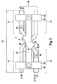
- the conductor element 18 is held in the region of the crossing 7 by an electrically non-conductive support apparatus 22, wherein the support apparatus 22 is supported on the two conductors 2 at its respective opposite ends with transverse elements 23.
- the cross members 23 extend transversely to the conductors 2 and act on these, for example on the upper side; In particular, it is possible to manufacture the cross members 23 made of plastic 24 and they resiliently put on the ladder 2 so that they rest on the ladders 2 by a clamping force applied over the resilient plastic 24. Between the two transverse elements 23, a boom 25 is arranged, in particular connected to the transverse elements 23 or formed integrally with the transverse elements 23.
- the arm 25 carries the conductor element 18.
- the conductor element 18 at least partially, namely in its central portion 26, surrounded by material of the arm 25, in particular with plastic 24 is encapsulated.
- the crossover 7 is in turn formed at least substantially in the electrical center of the electrical length 13 of the conductors 2.
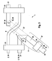
- FIG. 3 shows a line assembly 1 with two conductors 2, as already to FIG. 2 described, wherein the conductors 2 are formed as stamped lattice webs 15 and one of the two conductors 2 is guided S-shaped, that has an S-shaped configuration 6.
- the two conductors 2 are held by transverse elements 23 spaced from each other.
- the other conductor 20, which does not have the S-shaped configuration 6, is, as already in FIG. 2 described, guided substantially straight and interrupted, wherein a first conductor part 28 in approximately V-shaped over the longitudinal extent of the line assembly 1 also out approximately transversely and also provided with a plastic spacer 24 29 is provided.
- the first conductor part 28 has a right-angled branch 30 which extends the first conductor part 28 transversely to the axial extent of the other conductor 20.
- a right-angled branch 30 and a first rectangular extension then follows an angled branch 31, which is designed such that at kinking / deformation in the angled branch 31 beyond this protruding, the spacer element 29 carrying conductor rest 32 as bridge element 27 on the S-shaped training 6 extends and the spacer element 29 after kinking displacement of the conductor element 32 is located approximately above the S-shaped configuration 6 to prevent unwanted contact between the two conductors 2.
- connection 35 is made to form the connection point 19, for example, as a weld point 36.
- the shift in Direction of the arrow V in the angled branch 31, in particular by cold forming such as punching thus provides from the conductor rest 32, the bridge member 27 for connecting the other conductors 20, wherein the bridge member 27 integral with the other conductor 20, namely one of the conductor pieces 21, formed and connected to the other conductor piece 21 at the connection point 19, in particular welded to the weld point 36.
Landscapes
- Engineering & Computer Science (AREA)
- Manufacturing & Machinery (AREA)
- Physics & Mathematics (AREA)
- Electromagnetism (AREA)
- Microelectronics & Electronic Packaging (AREA)
- Structure Of Printed Boards (AREA)
Claims (10)
- Dispositif de câble électrique, servant notamment à une transmission de données, avec au moins deux conducteurs électriques guidés pour l'essentiel parallèlement, les conducteurs (2) possédant au moins une intersection (7) comportant au moins un élément conducteur (18) séparé, relié sur le plan électrique, les conducteurs (2) étant réalisés sur un substrat (5) flexible, caractérisé en ce que l'élément conducteur (18) séparé est maintenu au niveau des conducteurs (2, 20) à l'aide d'un appareil de maintien (22) électriquement non conducteur, l'appareil de maintien (22) comportant au moins un élément transversal (23) s'appuyant contre les deux conducteurs (2, 20) à une certaine distance de l'intersection (7) à l'aide d'un organe de serrage ainsi qu'un portant (25) auquel l'élément conducteur (18) séparé est fixé partant de l'élément transversal (23).
- Dispositif de câble selon la revendication 1, caractérisé en ce que l'intersection est réalisée dans ou pour l'essentiel dans le centre électrique d'une longueur électrique (13) des conducteurs (2).
- Dispositif de câble selon l'une quelconque des revendications précédentes, caractérisé en ce que les conducteurs (2) prennent la forme de pistes conductrices (12).
- Dispositif de câble selon l'une quelconque des revendications précédentes, caractérisé en ce que les conducteurs (2) prennent la forme de pistes de grille estampée (15).
- Dispositif de câble selon l'une quelconque des revendications précédentes, caractérisé en ce que les conducteurs (2) se trouvent sur un substrat de conducteur (4) électriquement non conducteur.
- Dispositif de câble selon l'une quelconque des revendications précédentes, caractérisé en ce qu'un des conducteur (2) est guidé en forme de S pour former l'intersection (7) et que l'autre conducteur (2, 20) est guidé tout droit jusqu'à l'intersection (7) et guidé de nouveau tout droit à partir de l'intersection (7) et que l'élément conducteur (18) séparé relie les deux pièces de conducteur (21) guidées tout droit et s'étendant en oblique dans la région en S du premier conducteur (2) et n'est pas relié sur le plan électrique avec ledit conducteur (2).
- Dispositif de câble selon l'une quelconque des revendications précédentes, caractérisé en ce que l'élément conducteur (18) séparé est relié sur le plan électrique aux pièces de conducteur (21), notamment soudé.
- Dispositif de câble selon l'une quelconque des revendications précédentes, caractérisé en ce que l'appareil de maintien (22) ou au moins une section (17) de celui-ci est fabriqué selon un procédé d'injection de matière plastique, notamment selon un procédé de moulage par injection de matière plastique.
- Dispositif de câble selon l'une quelconque des revendications précédentes, caractérisé en ce que l'élément conducteur (18) séparé est fabriqué d'un seul tenant avec une des deux pièces de conducteurs (21) guidées tout droit et déformé pour former l'intersection (7) et déplacé au moins par endroits.
- Dispositif de câble selon l'une quelconque des revendications précédentes, caractérisé en ce que le déplacement de l'élément conducteur (18) séparé est réalisé par le biais d'un processus de déformation, notamment une déformation à froid.
Applications Claiming Priority (1)
| Application Number | Priority Date | Filing Date | Title |
|---|---|---|---|
| DE200810042845 DE102008042845A1 (de) | 2008-10-15 | 2008-10-15 | Elektrische Leitungsanordnung |
Publications (2)
| Publication Number | Publication Date |
|---|---|
| EP2178154A1 EP2178154A1 (fr) | 2010-04-21 |
| EP2178154B1 true EP2178154B1 (fr) | 2013-05-22 |
Family
ID=41402228
Family Applications (1)
| Application Number | Title | Priority Date | Filing Date |
|---|---|---|---|
| EP20090172550 Not-in-force EP2178154B1 (fr) | 2008-10-15 | 2009-10-08 | Dispositif de ligne électrique |
Country Status (2)
| Country | Link |
|---|---|
| EP (1) | EP2178154B1 (fr) |
| DE (1) | DE102008042845A1 (fr) |
Cited By (1)
| Publication number | Priority date | Publication date | Assignee | Title |
|---|---|---|---|---|
| DE102021201446A1 (de) | 2021-02-16 | 2022-08-18 | Robert Bosch Gesellschaft mit beschränkter Haftung | Leitungsanordnung und Steuergerät mit einer Leitungsanordnung |
Family Cites Families (6)
| Publication number | Priority date | Publication date | Assignee | Title |
|---|---|---|---|---|
| FR1402897A (fr) * | 1964-03-06 | 1965-06-18 | Telecommunications Sa | Circuits à conducteurs plats pour câbles de télécommunication |
| JP2860468B2 (ja) * | 1996-05-24 | 1999-02-24 | モレックス インコーポレーテッド | 擬似ツイストペア平型柔軟ケーブル |
| DE19738754A1 (de) * | 1997-09-04 | 1999-03-11 | Delphi Automotive Systems Gmbh | Abgeschirmte elektrische Drähte |
| JP2001236479A (ja) * | 2000-02-22 | 2001-08-31 | Miyota Kk | 非接触型icカード |
| US7271985B1 (en) * | 2004-09-24 | 2007-09-18 | Storage Technology Corporation | System and method for crosstalk reduction in a flexible trace interconnect array |
| EP2068391A3 (fr) * | 2007-12-04 | 2010-01-20 | Rohde & Schwarz GmbH & Co. KG | Dispositif doté d'une ligne à bande croisée |
-
2008
- 2008-10-15 DE DE200810042845 patent/DE102008042845A1/de not_active Withdrawn
-
2009
- 2009-10-08 EP EP20090172550 patent/EP2178154B1/fr not_active Not-in-force
Cited By (1)
| Publication number | Priority date | Publication date | Assignee | Title |
|---|---|---|---|---|
| DE102021201446A1 (de) | 2021-02-16 | 2022-08-18 | Robert Bosch Gesellschaft mit beschränkter Haftung | Leitungsanordnung und Steuergerät mit einer Leitungsanordnung |
Also Published As
| Publication number | Publication date |
|---|---|
| EP2178154A1 (fr) | 2010-04-21 |
| DE102008042845A1 (de) | 2010-04-22 |
Similar Documents
| Publication | Publication Date | Title |
|---|---|---|
| DE19928788B4 (de) | Elektronisches Keramikbauelement | |
| DE112019002733B4 (de) | Verkabelungselement | |
| DE102017215419A1 (de) | Kondensatoreinheit und Baugruppe für eine Leistungselektronik | |
| DE112012001747T5 (de) | Stromanschlussschiene für die Verwendung in einem Elektromotor | |
| WO2011141314A1 (fr) | Système de barres omnibus à profilé de support | |
| DE102004006575A1 (de) | Leistungsverteiler für ein Kraftfahrzeug | |
| DE102015104297A1 (de) | Fixierelement zum Anbinden einer Platine, Stromschiene und damit ausgestatteter Stromverteiler eines Fahrzeugs | |
| DE102010039187A1 (de) | Elektrische Verbindungsanordnung | |
| WO2012152292A1 (fr) | Élément de contact électrique | |
| EP3010095B1 (fr) | Contact d'insertion | |
| EP1555865B1 (fr) | Assemblage d'un circuit bouchon avec des composants électroniques discrets et passifs | |
| DE112018005377B4 (de) | Mit einem Anschluss ausgerüsteter Draht | |
| DE102016002821A1 (de) | Schaltkreis einer elektronischen Steuereinheit | |
| DE102016110847B4 (de) | Leitungsintegrierter Schalter und Verfahren zum Herstellen eines leitungsintegrierten Schalters | |
| EP2178154A1 (fr) | Dispositif de ligne électrique | |
| WO2017178372A1 (fr) | Distributeur de courant pour un réseau de bord de véhicule et réseau de bord de véhicule associé | |
| DE102015106518A1 (de) | Elektrisches Bauteil | |
| EP4282034B1 (fr) | Dispositif connecteur d'alimentation pour cartes de circuit imprimé et procédé de montage d'un tel dispositif connecteur d'alimentation sur une carte de circuit imprimé | |
| DE102007003652B4 (de) | Elektrische Überbrückung | |
| EP2367202B1 (fr) | Procédé de fabrication d'une connexion électrique entre un contact et un contre-contact | |
| EP2932803B1 (fr) | Système de contact pour support de circuit multicouche | |
| DE102014107271B4 (de) | Halbleitermodul | |
| DE202011109444U1 (de) | Kontaktelement | |
| DE4238867C2 (de) | Vorrichtung und Verfahren zum Anschließen von mehreren elektrischen Verbrauchern | |
| EP3216329B1 (fr) | Procédé de fabrication d'un ensemble comprenant une pièce de boîtier et au moins deux rubans conducteurs |
Legal Events
| Date | Code | Title | Description |
|---|---|---|---|
| PUAI | Public reference made under article 153(3) epc to a published international application that has entered the european phase |
Free format text: ORIGINAL CODE: 0009012 |
|
| AK | Designated contracting states |
Kind code of ref document: A1 Designated state(s): AT BE BG CH CY CZ DE DK EE ES FI FR GB GR HR HU IE IS IT LI LT LU LV MC MK MT NL NO PL PT RO SE SI SK SM TR |
|
| AX | Request for extension of the european patent |
Extension state: AL BA RS |
|
| 17P | Request for examination filed |
Effective date: 20101021 |
|
| 17Q | First examination report despatched |
Effective date: 20101112 |
|
| GRAP | Despatch of communication of intention to grant a patent |
Free format text: ORIGINAL CODE: EPIDOSNIGR1 |
|
| GRAS | Grant fee paid |
Free format text: ORIGINAL CODE: EPIDOSNIGR3 |
|
| GRAA | (expected) grant |
Free format text: ORIGINAL CODE: 0009210 |
|
| AK | Designated contracting states |
Kind code of ref document: B1 Designated state(s): AT BE BG CH CY CZ DE DK EE ES FI FR GB GR HR HU IE IS IT LI LT LU LV MC MK MT NL NO PL PT RO SE SI SK SM TR |
|
| REG | Reference to a national code |
Ref country code: GB Ref legal event code: FG4D Free format text: NOT ENGLISH |
|
| REG | Reference to a national code |
Ref country code: CH Ref legal event code: EP |
|
| REG | Reference to a national code |
Ref country code: AT Ref legal event code: REF Ref document number: 613648 Country of ref document: AT Kind code of ref document: T Effective date: 20130615 |
|
| REG | Reference to a national code |
Ref country code: IE Ref legal event code: FG4D Free format text: LANGUAGE OF EP DOCUMENT: GERMAN |
|
| REG | Reference to a national code |
Ref country code: DE Ref legal event code: R096 Ref document number: 502009007148 Country of ref document: DE Effective date: 20130718 |
|
| REG | Reference to a national code |
Ref country code: LT Ref legal event code: MG4D |
|
| PG25 | Lapsed in a contracting state [announced via postgrant information from national office to epo] |
Ref country code: ES Free format text: LAPSE BECAUSE OF FAILURE TO SUBMIT A TRANSLATION OF THE DESCRIPTION OR TO PAY THE FEE WITHIN THE PRESCRIBED TIME-LIMIT Effective date: 20130902 Ref country code: IS Free format text: LAPSE BECAUSE OF FAILURE TO SUBMIT A TRANSLATION OF THE DESCRIPTION OR TO PAY THE FEE WITHIN THE PRESCRIBED TIME-LIMIT Effective date: 20130922 Ref country code: LT Free format text: LAPSE BECAUSE OF FAILURE TO SUBMIT A TRANSLATION OF THE DESCRIPTION OR TO PAY THE FEE WITHIN THE PRESCRIBED TIME-LIMIT Effective date: 20130522 Ref country code: FI Free format text: LAPSE BECAUSE OF FAILURE TO SUBMIT A TRANSLATION OF THE DESCRIPTION OR TO PAY THE FEE WITHIN THE PRESCRIBED TIME-LIMIT Effective date: 20130522 Ref country code: NO Free format text: LAPSE BECAUSE OF FAILURE TO SUBMIT A TRANSLATION OF THE DESCRIPTION OR TO PAY THE FEE WITHIN THE PRESCRIBED TIME-LIMIT Effective date: 20130822 Ref country code: SI Free format text: LAPSE BECAUSE OF FAILURE TO SUBMIT A TRANSLATION OF THE DESCRIPTION OR TO PAY THE FEE WITHIN THE PRESCRIBED TIME-LIMIT Effective date: 20130522 Ref country code: GR Free format text: LAPSE BECAUSE OF FAILURE TO SUBMIT A TRANSLATION OF THE DESCRIPTION OR TO PAY THE FEE WITHIN THE PRESCRIBED TIME-LIMIT Effective date: 20130823 Ref country code: SE Free format text: LAPSE BECAUSE OF FAILURE TO SUBMIT A TRANSLATION OF THE DESCRIPTION OR TO PAY THE FEE WITHIN THE PRESCRIBED TIME-LIMIT Effective date: 20130522 Ref country code: PT Free format text: LAPSE BECAUSE OF FAILURE TO SUBMIT A TRANSLATION OF THE DESCRIPTION OR TO PAY THE FEE WITHIN THE PRESCRIBED TIME-LIMIT Effective date: 20130923 |
|
| REG | Reference to a national code |
Ref country code: NL Ref legal event code: VDEP Effective date: 20130522 |
|
| PG25 | Lapsed in a contracting state [announced via postgrant information from national office to epo] |
Ref country code: PL Free format text: LAPSE BECAUSE OF FAILURE TO SUBMIT A TRANSLATION OF THE DESCRIPTION OR TO PAY THE FEE WITHIN THE PRESCRIBED TIME-LIMIT Effective date: 20130522 Ref country code: BG Free format text: LAPSE BECAUSE OF FAILURE TO SUBMIT A TRANSLATION OF THE DESCRIPTION OR TO PAY THE FEE WITHIN THE PRESCRIBED TIME-LIMIT Effective date: 20130822 Ref country code: HR Free format text: LAPSE BECAUSE OF FAILURE TO SUBMIT A TRANSLATION OF THE DESCRIPTION OR TO PAY THE FEE WITHIN THE PRESCRIBED TIME-LIMIT Effective date: 20130522 |
|
| PG25 | Lapsed in a contracting state [announced via postgrant information from national office to epo] |
Ref country code: LV Free format text: LAPSE BECAUSE OF FAILURE TO SUBMIT A TRANSLATION OF THE DESCRIPTION OR TO PAY THE FEE WITHIN THE PRESCRIBED TIME-LIMIT Effective date: 20130522 |
|
| PG25 | Lapsed in a contracting state [announced via postgrant information from national office to epo] |
Ref country code: CZ Free format text: LAPSE BECAUSE OF FAILURE TO SUBMIT A TRANSLATION OF THE DESCRIPTION OR TO PAY THE FEE WITHIN THE PRESCRIBED TIME-LIMIT Effective date: 20130522 Ref country code: DK Free format text: LAPSE BECAUSE OF FAILURE TO SUBMIT A TRANSLATION OF THE DESCRIPTION OR TO PAY THE FEE WITHIN THE PRESCRIBED TIME-LIMIT Effective date: 20130522 Ref country code: EE Free format text: LAPSE BECAUSE OF FAILURE TO SUBMIT A TRANSLATION OF THE DESCRIPTION OR TO PAY THE FEE WITHIN THE PRESCRIBED TIME-LIMIT Effective date: 20130522 Ref country code: SK Free format text: LAPSE BECAUSE OF FAILURE TO SUBMIT A TRANSLATION OF THE DESCRIPTION OR TO PAY THE FEE WITHIN THE PRESCRIBED TIME-LIMIT Effective date: 20130522 |
|
| PG25 | Lapsed in a contracting state [announced via postgrant information from national office to epo] |
Ref country code: NL Free format text: LAPSE BECAUSE OF FAILURE TO SUBMIT A TRANSLATION OF THE DESCRIPTION OR TO PAY THE FEE WITHIN THE PRESCRIBED TIME-LIMIT Effective date: 20130522 Ref country code: RO Free format text: LAPSE BECAUSE OF FAILURE TO SUBMIT A TRANSLATION OF THE DESCRIPTION OR TO PAY THE FEE WITHIN THE PRESCRIBED TIME-LIMIT Effective date: 20130522 |
|
| PLBE | No opposition filed within time limit |
Free format text: ORIGINAL CODE: 0009261 |
|
| STAA | Information on the status of an ep patent application or granted ep patent |
Free format text: STATUS: NO OPPOSITION FILED WITHIN TIME LIMIT |
|
| 26N | No opposition filed |
Effective date: 20140225 |
|
| BERE | Be: lapsed |
Owner name: ROBERT BOSCH G.M.B.H. Effective date: 20131031 |
|
| PG25 | Lapsed in a contracting state [announced via postgrant information from national office to epo] |
Ref country code: MC Free format text: LAPSE BECAUSE OF FAILURE TO SUBMIT A TRANSLATION OF THE DESCRIPTION OR TO PAY THE FEE WITHIN THE PRESCRIBED TIME-LIMIT Effective date: 20130522 |
|
| REG | Reference to a national code |
Ref country code: CH Ref legal event code: PL |
|
| REG | Reference to a national code |
Ref country code: DE Ref legal event code: R097 Ref document number: 502009007148 Country of ref document: DE Effective date: 20140225 |
|
| REG | Reference to a national code |
Ref country code: IE Ref legal event code: MM4A |
|
| PG25 | Lapsed in a contracting state [announced via postgrant information from national office to epo] |
Ref country code: LI Free format text: LAPSE BECAUSE OF NON-PAYMENT OF DUE FEES Effective date: 20131031 Ref country code: CH Free format text: LAPSE BECAUSE OF NON-PAYMENT OF DUE FEES Effective date: 20131031 |
|
| PG25 | Lapsed in a contracting state [announced via postgrant information from national office to epo] |
Ref country code: BE Free format text: LAPSE BECAUSE OF NON-PAYMENT OF DUE FEES Effective date: 20131031 |
|
| PG25 | Lapsed in a contracting state [announced via postgrant information from national office to epo] |
Ref country code: IE Free format text: LAPSE BECAUSE OF NON-PAYMENT OF DUE FEES Effective date: 20131008 |
|
| PG25 | Lapsed in a contracting state [announced via postgrant information from national office to epo] |
Ref country code: SM Free format text: LAPSE BECAUSE OF FAILURE TO SUBMIT A TRANSLATION OF THE DESCRIPTION OR TO PAY THE FEE WITHIN THE PRESCRIBED TIME-LIMIT Effective date: 20130522 |
|
| PG25 | Lapsed in a contracting state [announced via postgrant information from national office to epo] |
Ref country code: TR Free format text: LAPSE BECAUSE OF FAILURE TO SUBMIT A TRANSLATION OF THE DESCRIPTION OR TO PAY THE FEE WITHIN THE PRESCRIBED TIME-LIMIT Effective date: 20130522 Ref country code: CY Free format text: LAPSE BECAUSE OF FAILURE TO SUBMIT A TRANSLATION OF THE DESCRIPTION OR TO PAY THE FEE WITHIN THE PRESCRIBED TIME-LIMIT Effective date: 20130522 |
|
| PG25 | Lapsed in a contracting state [announced via postgrant information from national office to epo] |
Ref country code: HU Free format text: LAPSE BECAUSE OF FAILURE TO SUBMIT A TRANSLATION OF THE DESCRIPTION OR TO PAY THE FEE WITHIN THE PRESCRIBED TIME-LIMIT; INVALID AB INITIO Effective date: 20091008 Ref country code: MK Free format text: LAPSE BECAUSE OF FAILURE TO SUBMIT A TRANSLATION OF THE DESCRIPTION OR TO PAY THE FEE WITHIN THE PRESCRIBED TIME-LIMIT Effective date: 20130522 Ref country code: LU Free format text: LAPSE BECAUSE OF NON-PAYMENT OF DUE FEES Effective date: 20131008 |
|
| PG25 | Lapsed in a contracting state [announced via postgrant information from national office to epo] |
Ref country code: MT Free format text: LAPSE BECAUSE OF FAILURE TO SUBMIT A TRANSLATION OF THE DESCRIPTION OR TO PAY THE FEE WITHIN THE PRESCRIBED TIME-LIMIT Effective date: 20130522 |
|
| REG | Reference to a national code |
Ref country code: FR Ref legal event code: PLFP Year of fee payment: 7 |
|
| REG | Reference to a national code |
Ref country code: AT Ref legal event code: MM01 Ref document number: 613648 Country of ref document: AT Kind code of ref document: T Effective date: 20141008 |
|
| PG25 | Lapsed in a contracting state [announced via postgrant information from national office to epo] |
Ref country code: AT Free format text: LAPSE BECAUSE OF NON-PAYMENT OF DUE FEES Effective date: 20141008 |
|
| REG | Reference to a national code |
Ref country code: FR Ref legal event code: PLFP Year of fee payment: 8 |
|
| REG | Reference to a national code |
Ref country code: FR Ref legal event code: PLFP Year of fee payment: 9 |
|
| REG | Reference to a national code |
Ref country code: FR Ref legal event code: PLFP Year of fee payment: 10 |
|
| PGFP | Annual fee paid to national office [announced via postgrant information from national office to epo] |
Ref country code: DE Payment date: 20181206 Year of fee payment: 10 |
|
| PGFP | Annual fee paid to national office [announced via postgrant information from national office to epo] |
Ref country code: IT Payment date: 20191021 Year of fee payment: 11 Ref country code: FR Payment date: 20191022 Year of fee payment: 11 |
|
| PGFP | Annual fee paid to national office [announced via postgrant information from national office to epo] |
Ref country code: GB Payment date: 20191023 Year of fee payment: 11 |
|
| REG | Reference to a national code |
Ref country code: DE Ref legal event code: R119 Ref document number: 502009007148 Country of ref document: DE |
|
| PG25 | Lapsed in a contracting state [announced via postgrant information from national office to epo] |
Ref country code: DE Free format text: LAPSE BECAUSE OF NON-PAYMENT OF DUE FEES Effective date: 20200501 |
|
| GBPC | Gb: european patent ceased through non-payment of renewal fee |
Effective date: 20201008 |
|
| PG25 | Lapsed in a contracting state [announced via postgrant information from national office to epo] |
Ref country code: FR Free format text: LAPSE BECAUSE OF NON-PAYMENT OF DUE FEES Effective date: 20201031 |
|
| PG25 | Lapsed in a contracting state [announced via postgrant information from national office to epo] |
Ref country code: GB Free format text: LAPSE BECAUSE OF NON-PAYMENT OF DUE FEES Effective date: 20201008 |
|
| PG25 | Lapsed in a contracting state [announced via postgrant information from national office to epo] |
Ref country code: IT Free format text: LAPSE BECAUSE OF NON-PAYMENT OF DUE FEES Effective date: 20201008 |