EP2178207A1 - Resonator und filter mit benutzung desselben - Google Patents
Resonator und filter mit benutzung desselben Download PDFInfo
- Publication number
- EP2178207A1 EP2178207A1 EP08828167A EP08828167A EP2178207A1 EP 2178207 A1 EP2178207 A1 EP 2178207A1 EP 08828167 A EP08828167 A EP 08828167A EP 08828167 A EP08828167 A EP 08828167A EP 2178207 A1 EP2178207 A1 EP 2178207A1
- Authority
- EP
- European Patent Office
- Prior art keywords
- impedance wiring
- low
- impedance
- wiring
- columnar conductor
- Prior art date
- Legal status (The legal status is an assumption and is not a legal conclusion. Google has not performed a legal analysis and makes no representation as to the accuracy of the status listed.)
- Withdrawn
Links
Images






Classifications
-
- H—ELECTRICITY
- H01—ELECTRIC ELEMENTS
- H01P—WAVEGUIDES; RESONATORS, LINES, OR OTHER DEVICES OF THE WAVEGUIDE TYPE
- H01P7/00—Resonators of the waveguide type
- H01P7/08—Strip line resonators
- H01P7/084—Triplate line resonators
-
- H—ELECTRICITY
- H01—ELECTRIC ELEMENTS
- H01P—WAVEGUIDES; RESONATORS, LINES, OR OTHER DEVICES OF THE WAVEGUIDE TYPE
- H01P1/00—Auxiliary devices
- H01P1/20—Frequency-selective devices, e.g. filters
- H01P1/201—Filters for transverse electromagnetic waves
- H01P1/203—Strip line filters
- H01P1/20327—Electromagnetic interstage coupling
- H01P1/20354—Non-comb or non-interdigital filters
- H01P1/20372—Hairpin resonators
-
- H—ELECTRICITY
- H01—ELECTRIC ELEMENTS
- H01P—WAVEGUIDES; RESONATORS, LINES, OR OTHER DEVICES OF THE WAVEGUIDE TYPE
- H01P1/00—Auxiliary devices
- H01P1/20—Frequency-selective devices, e.g. filters
- H01P1/201—Filters for transverse electromagnetic waves
- H01P1/203—Strip line filters
- H01P1/20327—Electromagnetic interstage coupling
- H01P1/20354—Non-comb or non-interdigital filters
- H01P1/20381—Special shape resonators
Definitions
- the present invention relates to a resonator used for various types of electronic appliances such as a mobile phone and to a filter and an electronic device including the resonator.
- Figure 12 is a top view of a conventional resonator.
- one end of low-impedance wiring 1a is electrically connected to one end of high-impedance wiring 2a.
- one end of low-impedance wiring 1b is electrically connected to one end of high-impedance wiring 2b.
- the other end of high-impedance wiring 2a is electrically connected to the other end of high-impedance wiring 2b.
- Prior art documents on this patent application include patent literature 1, for instance.
- the area size of the resonator is given by summing the area sizes of four wiring 1a, 1b, 2a, 2b. Accordingly, reducing the area size of a resonator is difficult.
- the present invention helps reduce the area size of a resonator.
- a resonator of the present invention includes a top-surface ground electrode; a plate-like first high-impedance wiring arranged parallel to the top-surface ground electrode; a plate-like second high-impedance wiring arranged so as to face the first high-impedance wiring; a first columnar conductor electrically connecting the first high-impedance wiring to the second high; a first low-impedance wiring arranged between the first and second high-impedance wiring; a second columnar conductor electrically connecting the first high-impedance wiring to the first low; and a third columnar conductor electrically connecting the second high-impedance wiring to the second low.
- Such a configuration allows the resonator to be structured three-dimensionally.
- the area size of a resonator is reduced by making the size smaller than the sum of the area sizes of the first and second high-impedance wiring, and the first and second low-impedance wiring.
- FIG. 1 is a perspective view of a resonator according to the first exemplary embodiment of the present invention.
- the resonator according to the first embodiment has top-surface ground electrode 4 on the top surface of dielectric laminated substrate 3 and bottom-surface ground electrode 5 on the bottom surface of dielectric laminated substrate 3, each arranged so as to face the other.
- the inside of dielectric laminated substrate 3 interposed between top-surface ground electrode 4 and bottom-surface ground electrode 5 contains first and second high-impedance wiring 7a, 7b; first and second low-impedance wiring 8a, 8b; and first, second, and third columnar conductors 9a, 9b, 9c.
- First and second high-impedance wiring 7a, 7b are respectively arranged so as to face top- and bottom-surface ground electrodes 4, 5.
- first and second low-impedance wiring 8a, 8b are respectively arranged so as to face top- and bottom-surface ground electrodes 4, 5.
- First high-impedance wiring 7a is arranged near and parallel to top-surface ground electrode 4.
- Second high-impedance wiring 7b is arranged near and parallel to bottom-surface ground electrode 5.
- First high-impedance wiring 7a is arranged so as to face second high-impedance wiring 7b.
- first columnar conductor 9a is connected to one end of first high-impedance wiring 7a and to one end of second high-impedance wiring 7b (both at the same side).
- second columnar conductor 9b is made equal to that of third columnar conductor 9c.
- Second and third columnar conductor 9b, 9 are arranged on the same straight line.
- the length of the first columnar conductor is larger than the sum of the lengths of the second and third columnar conductors.
- first high-impedance wiring 7a is connected to one end of first low-impedance wiring 8a arranged so as to face first high-impedance wiring 7a through second columnar conductor 9b.
- the other end of first low-impedance wiring 8a is open with nothing connected thereto. In other words, first columnar conductor 9a is not electrically connected to first low-impedance wiring 8a.
- Second low-impedance wiring 8b is arranged so as to face first low-impedance wiring 8a. Then, the other end of second low-impedance wiring 8b is connected to the other end of second high-impedance wiring 7b through third columnar conductor 9c. First low-impedance wiring 8a is not electrically connected to second low-impedance wiring 8b. The one end of second low-impedance wiring 8b is open with nothing connected thereto. In other words, first columnar conductor 9a is not electrically connected to second low-impedance wiring 8b.
- Figure 2A is a sectional view of the resonator according to the first embodiment of the present invention.
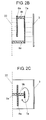
- Figure 2B is an enlarged figure of one half side of the sectional view of the resonator according to the first embodiment of the present invention.
- Figure 2C is a sectional view of FIG. 2B viewed from the top surface.
- the resonator according to the first embodiment of the present invention is supposed to have virtual ground surface 22 (shown by the dashed-dotted line) with the center between first low-impedance wiring 8a and second low-impedance wiring 8b being a boundary. Accordingly, electric flux lines from first low-impedance wiring 8a and second low-impedance wiring 8b occur to virtual ground surface 22 (refer to FIG.
- first low-impedance wiring 8a is determined by the distance between first low-impedance wiring 8a and virtual ground surface 22.
- impedance of second low-impedance wiring 8b is determined by the distance between second low-impedance wiring 8b and virtual ground surface 22.
- first high-impedance wiring 7a occurs to top-surface ground electrode 4 as shown by the broken lines in FIG. 2B . Consequently, the impedance of first high-impedance wiring 7a is determined by the distance between first high-impedance wiring 7a and top-surface ground electrode 4. In the same way, electric flux lines from second high-impedance wiring 7b occur to bottom-surface ground electrode 5. Consequently, the impedance of second high-impedance wiring 7b is determined by the distance between second high-impedance wiring 7b and bottom-surface ground electrode 5.
- first high-impedance wiring 7a and first low-impedance wiring 8a Currents flow in opposite directions between first high-impedance wiring 7a and first low-impedance wiring 8a; and second high-impedance wiring 7b and second low-impedance wiring 8b.
- the line width of first high-impedance wiring 7a is different from that of first low-impedance wiring 8a, for instance, and thus a current generated in first high-impedance wiring 7a is not completely canceled by that in first low-impedance wiring 8a. Consequently, magnetic force lines occur as shown by the solid line in FIG. 2C to influence each impedance.
- the line width of the first high-impedance wiring may be made smaller than that of the first low-impedance wiring.
- the line width of the second high-impedance wiring may be made smaller than that of the second low-impedance wiring.
- first and second high-impedance wiring 7a, 7b are respectively determined by the distance to top-surface ground electrode 4 and to bottom-surface ground electrode 5, namely the conductor length of first columnar conductor 9a. Accordingly, the resonance frequency of the resonator according to the first embodiment of the present invention can be controlled.
- first low-impedance wiring 8a and virtual ground surface 22 is determined by the conductor length of second columnar conductor 9b.
- the distance between second low-impedance wiring 8b and virtual ground surface 22 is determined by the conductor length of third columnar conductor 9c. Accordingly, the resonance frequency of the resonator according to the first embodiment of the present invention can be controlled.
- a half-wavelength resonator can be structured three-dimensionally, and thus the area size of the resonator can be made smaller than the sum of the area sizes of first high-impedance wiring 7a, second high-impedance wiring 7b, first low-impedance wiring 8a, and second low-impedance wiring 8b. Consequently, the area size of a resonator can be reduced.
- first high-impedance wiring 7a and second high-impedance wiring 7b is 200 ⁇ m; the line length, 775 ⁇ m; and the line thickness, 10 ⁇ m.
- the line width of first low-impedance wiring 8a and second low-impedance wiring 8b is 600 ⁇ m; the line length, 1,025 ⁇ m; and the line thickness, 10 ⁇ m.
- first low-impedance wiring 8a and second low-impedance wiring 8b are made agree with the center of the thickness of the dielectric laminated substrate.
- the diameter of each of first columnar conductor 9a, second columnar conductor 9b, and third columnar conductor 9c is 100 ⁇ m.
- FIG. 3 is a perspective view showing an example configuration for characterizing the resonator according to the first embodiment of the present invention.
- I/O terminals 10a, 10b placed at bottom-surface ground electrode 5 are provided therefrom with I/O wiring 12a, 12b through columnar conductors 11a, 11b.
- I/O wiring 12a, 12b are respectively arranged so as to capacitively couple to the open ends of first low-impedance wiring 8a and second low-impedance wiring 8b at an interval of 20 ⁇ m in an area size of 200 ⁇ m by 100 ⁇ m.
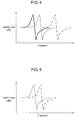
- Figure 4 is a characteristic diagram of the resonator according to the first embodiment of the present invention.
- the conductor length of first columnar conductor 9a is variable (140, 260, 380 ⁇ m).
- the length of 140 ⁇ m corresponds to the solid line; 260 ⁇ m, broken line; and 380 ⁇ m, dashed-dotted line.
- increasing the conductor length of first columnar conductor 9a raises the resonance frequency of the resonator.
- Figure 5 is another characteristic diagram of the resonator according to the first embodiment of the present invention.
- the conductor length of first columnar conductor 9a is fixed to 380 ⁇ m, while those of second columnar conductor 9b and third columnar conductor 9c are variable (110 ⁇ m and 140 ⁇ m respectively).
- the length of 110 ⁇ m corresponds to the broken line; and 140 ⁇ m, dashed-dotted line.
- extending second columnar conductor 9b and third columnar conductor 9c raises the resonance frequency of the resonator.
- first columnar conductor 9a second columnar conductor 9b, and third columnar conductor 9c allows controlling the resonance frequency.
- FIG. 6 is a perspective view of another resonator according to the first embodiment of the present invention.
- loading capacitance 20a is provided between first low-impedance wiring 8a and first high-impedance wiring 7a, at the open end of first low-impedance wiring 8a.
- Loading capacitance 20b is provided between second low-impedance wiring 8b and second high-impedance wiring 7b, at the open end of second low-impedance wiring 8b.
- both top-surface ground electrode 4 and bottom-surface ground electrode 5 are desirably connected to side-surface ground electrodes 6a, 6b electrically.
- the same effect is provided even if top-surface ground electrode 4 is electrically connected to bottom-surface ground electrode 5 using a columnar conductor instead of side-surface ground electrodes 6a, 6b.
- first high-impedance wiring 7a is different from second high-impedance wiring 7b in shape; first low-impedance wiring 8a is different from second low-impedance wiring 8b in shape, which allows a coupling device for such as I/O coupling and interstage coupling to be provided more easily.
- second columnar conductor 9b is different from third columnar conductor 9c in conductor length, which allows a coupling device for such as I/O coupling and interstage coupling to be provided more easily. That is, such an asymmetric structure allows correcting fluctuation in impedance of the resonator caused by a coupling device.
- Figure 7 is a perspective view showing another embodiment of the resonator according to the first embodiment of the present invention.
- enlarging the shape of bottom-surface ground electrode 5 provides a more stable ground surface.
- FIG. 8 is a perspective view showing a filter including the resonator according to the first embodiment of the present invention.
- two or more resonators of the present invention are used; they are connected with each other through electromagnetic field coupling by interstage coupling device 23; and by input coupling devices 24a, 24b and output coupling devices 25a, 25b.
- interstage coupling device 23 input coupling devices 24a, 24b and output coupling devices 25a, 25b.
- Incorporating such a filter further reduces the size of an electronic device contained in a mobile phone and other appliances.
- FIG. 9 is a perspective view of a resonator according to the second exemplary embodiment of the present invention.
- the top and bottom surfaces of dielectric laminated substrate 13 respectively have top-surface ground electrode 14 and bottom-surface ground electrode 15 arranged thereon so as to face each other.
- the inside of dielectric laminated substrate 13 interposed between top-surface ground electrode 14 and bottom-surface ground electrode 15 contains first high-impedance wiring 17a, second high-impedance wiring 17b, first low-impedance wiring 18a, second low-impedance wiring 18b, first columnar conductor 19a, second columnar conductor 19b, and third columnar conductor 19c.
- First high-impedance wiring 17a and second high-impedance wiring 17b are arranged so as to face top-surface ground electrode 14 and bottom-surface ground electrode 15, respectively.
- first low-impedance wiring 18a and second low-impedance wiring 18b are arranged so as to face top-surface ground electrode 14 and bottom-surface ground electrode 15, respectively.
- First high-impedance wiring 17a is arranged near and parallel to top-surface ground electrode 14.
- Second high-impedance wiring 17b is arranged near and parallel to bottom-surface ground electrode 15.
- First high-impedance wiring 17a and second high-impedance wiring 17b are arranged facing each other.
- first columnar conductor 19a is connected to one end of first high-impedance wiring 17a and to one end of second high-impedance wiring 17b (both at the same side).
- the second embodiment of the present invention is different from the first in the following points. That is, the other end of first high-impedance wiring 17a is connected to one end of first low-impedance wiring 18a arranged parallel to and not facing first high-impedance wiring 17a through second columnar conductor 19b. Similarly, the other end of second high-impedance wiring 17b is connected to one end of second low-impedance wiring 18b arranged parallel to and not facing second high-impedance wiring 17b through third columnar conductor 19c.
- electromagnetic field coupling can be avoided between first high-impedance wiring 17a and first low-impedance wiring 18a.
- electromagnetic field coupling can be avoided between second high-impedance wiring 17b and second low-impedance wiring 18b. Accordingly, a resonator can be designed easily.
- second low-impedance wiring 18b is arranged so as to face first low-impedance wiring 18a.
- the other end of first low-impedance wiring 18a is open with nothing connected thereto.
- the other end of second low-impedance wiring 18b is open with nothing connected thereto.
- the operation principle of the resonator according to the second embodiment of the present invention is the same as that of the first embodiment. Specifically, the resonance frequency of a resonator can be adjusted by adjusting the conductor lengths of first columnar conductor 19a, second columnar conductor 19b, and third columnar conductor 19c.
- a half-wavelength resonator can be structured three-dimensionally, thereby reducing the area size of the resonator.
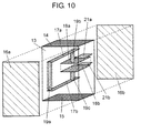
- FIG. 10 is a perspective view of another resonator according to the second embodiment of the present invention.
- loading capacitance 21a is provided between first low-impedance wiring 18a and first high-impedance wiring 17a, at the open end of first low-impedance wiring 18a.
- loading capacitance 21b is provided between second low-impedance wiring 18b and second high-impedance wiring 17b, at the open end of second low-impedance wiring 18b.
- side-surface ground electrodes 16a, 16b, top-surface ground electrode 14, and bottom-surface ground electrode 15 are desirably connected to each other electrically. The same effect is provided even if top-surface ground electrode 4 is electrically connected to bottom-surface ground electrode 15 using a columnar conductor instead of side-surface ground electrodes 16a, 16b.
- first high-impedance wiring 17a is different from second high-impedance wiring 17b in shape; first low-impedance wiring 18a is different from second low-impedance wiring 18b in shape, which allows a coupling device for such as I/O coupling and interstage coupling to be provided more easily.
- second columnar conductor 19b is different from third columnar conductor 19c in conductor length, which allows a coupling device for such as I/O coupling and interstage coupling to be provided more easily. That is, such an asymmetric structure allows correcting fluctuation in impedance of the resonator caused by a coupling device.
- Figure 11 is a perspective view showing another resonator according to the second embodiment of the present invention.
- enlarging the shape of bottom-surface ground electrode 15 provides a more stable ground surface.
- a resonator of the present invention provides an effect that reduces the area size and is useful for various types of electronic appliances such as a mobile phone.
Landscapes
- Physics & Mathematics (AREA)
- Electromagnetism (AREA)
- Control Of Motors That Do Not Use Commutators (AREA)
Applications Claiming Priority (2)
| Application Number | Priority Date | Filing Date | Title |
|---|---|---|---|
| JP2007217941A JP5061794B2 (ja) | 2007-08-24 | 2007-08-24 | 共振器とそれを用いたフィルタおよび電子機器 |
| PCT/JP2008/002247 WO2009028153A1 (ja) | 2007-08-24 | 2008-08-20 | 共振器とそれを用いたフィルタ |
Publications (2)
| Publication Number | Publication Date |
|---|---|
| EP2178207A1 true EP2178207A1 (de) | 2010-04-21 |
| EP2178207A4 EP2178207A4 (de) | 2011-12-28 |
Family
ID=40386896
Family Applications (1)
| Application Number | Title | Priority Date | Filing Date |
|---|---|---|---|
| EP08828167A Withdrawn EP2178207A4 (de) | 2007-08-24 | 2008-08-20 | Resonator und filter mit benutzung desselben |
Country Status (5)
| Country | Link |
|---|---|
| US (1) | US8248190B2 (de) |
| EP (1) | EP2178207A4 (de) |
| JP (1) | JP5061794B2 (de) |
| CN (1) | CN101790844B (de) |
| WO (1) | WO2009028153A1 (de) |
Cited By (1)
| Publication number | Priority date | Publication date | Assignee | Title |
|---|---|---|---|---|
| TWI850812B (zh) * | 2021-10-26 | 2024-08-01 | 日商Tdk股份有限公司 | 積層型濾波器裝置 |
Families Citing this family (1)
| Publication number | Priority date | Publication date | Assignee | Title |
|---|---|---|---|---|
| CN117913486B (zh) * | 2024-03-19 | 2024-05-28 | 微网优联科技(成都)有限公司 | 一种低插损低成本多零点的小型化微带滤波器 |
Family Cites Families (18)
| Publication number | Priority date | Publication date | Assignee | Title |
|---|---|---|---|---|
| JPS6243909A (ja) * | 1985-08-22 | 1987-02-25 | Murata Mfg Co Ltd | 共振器およびそれを用いたフイルタ |
| JPH0510411Y2 (de) * | 1986-11-04 | 1993-03-15 | ||
| JPH02249303A (ja) * | 1989-03-23 | 1990-10-05 | Matsushita Electric Ind Co Ltd | ストリップ線路共振器 |
| GB2222312B (en) | 1988-08-04 | 1993-05-26 | Matsushita Electric Industrial Co Ltd | A resonator and a filter including the same |
| KR930703715A (ko) * | 1991-11-12 | 1993-11-30 | 다쯔타 도키오 | 접어진 스트립 선로형 유전체 공진기 및 그것을 사용한 적층형 유전체 필터 |
| EP0893839B1 (de) * | 1997-01-07 | 2007-08-15 | Matsushita Electric Industrial Co., Ltd. | Mehrschichtiges filter |
| JP3329235B2 (ja) * | 1997-06-24 | 2002-09-30 | 松下電器産業株式会社 | フィルタ |
| JPH11186807A (ja) * | 1997-12-17 | 1999-07-09 | Tdk Corp | 積層バンドパスフィルタとその帯域幅制御方法 |
| DE60138107D1 (de) * | 2000-07-24 | 2009-05-07 | Panasonic Corp | Laminiertes bandpasfilter, hochfrequenzfunkgerät und herstellungsverfahrenfür laminiertes abndpassfilter |
| US6771147B2 (en) * | 2001-12-17 | 2004-08-03 | Remec, Inc. | 1-100 GHz microstrip filter |
| JP3649183B2 (ja) | 2001-12-27 | 2005-05-18 | ソニー株式会社 | フィルタ回路装置及びその製造方法 |
| JP4047640B2 (ja) * | 2002-06-25 | 2008-02-13 | 京セラ株式会社 | 多層回路基板 |
| JP4155883B2 (ja) * | 2003-07-25 | 2008-09-24 | Tdk株式会社 | 積層型バンドパスフィルタ |
| JP2005057531A (ja) * | 2003-08-05 | 2005-03-03 | Denso Corp | フィルタ |
| US7102470B2 (en) | 2004-11-02 | 2006-09-05 | Integrated System Solution Corp. | Dual-band bandpass filter with stepped-impedance resonators |
| JP4339819B2 (ja) * | 2005-05-25 | 2009-10-07 | アルプス電気株式会社 | ハイパスフィルタ |
| US7312676B2 (en) * | 2005-07-01 | 2007-12-25 | Tdk Corporation | Multilayer band pass filter |
| US7525711B1 (en) * | 2005-08-31 | 2009-04-28 | The United States Of America As Represented By The Secretary Of The Navy | Actively tunable electromagnetic metamaterial |
-
2007
- 2007-08-24 JP JP2007217941A patent/JP5061794B2/ja not_active Expired - Fee Related
-
2008
- 2008-08-20 EP EP08828167A patent/EP2178207A4/de not_active Withdrawn
- 2008-08-20 US US12/674,078 patent/US8248190B2/en not_active Expired - Fee Related
- 2008-08-20 CN CN2008801042678A patent/CN101790844B/zh not_active Expired - Fee Related
- 2008-08-20 WO PCT/JP2008/002247 patent/WO2009028153A1/ja not_active Ceased
Cited By (2)
| Publication number | Priority date | Publication date | Assignee | Title |
|---|---|---|---|---|
| TWI850812B (zh) * | 2021-10-26 | 2024-08-01 | 日商Tdk股份有限公司 | 積層型濾波器裝置 |
| US12308502B2 (en) | 2021-10-26 | 2025-05-20 | Tdk Corporation | Multilayered filter device |
Also Published As
| Publication number | Publication date |
|---|---|
| US20100201460A1 (en) | 2010-08-12 |
| JP2009055161A (ja) | 2009-03-12 |
| JP5061794B2 (ja) | 2012-10-31 |
| WO2009028153A1 (ja) | 2009-03-05 |
| EP2178207A4 (de) | 2011-12-28 |
| CN101790844B (zh) | 2013-08-21 |
| CN101790844A (zh) | 2010-07-28 |
| US8248190B2 (en) | 2012-08-21 |
Similar Documents
| Publication | Publication Date | Title |
|---|---|---|
| US9000864B2 (en) | Directional coupler | |
| US6661640B2 (en) | Multilayer ceramic electronic device | |
| US7902944B2 (en) | Stacked resonator | |
| US11469483B2 (en) | Filter | |
| US11601108B2 (en) | Isolator and communication system | |
| JP2007013962A (ja) | 多層帯域通過フィルタ | |
| JP2017531959A (ja) | 多重モード共振器 | |
| JP2018196082A (ja) | 共振器 | |
| US7671704B2 (en) | LC resonant circuit | |
| KR20090088336A (ko) | 적층 콘덴서 | |
| US8823216B2 (en) | Signal transmission device, filter, and inter-substrate communication device | |
| JPWO2006011382A1 (ja) | 2ポート型アイソレータ及び通信装置 | |
| US8248190B2 (en) | Resonator and filter using the same | |
| JP6868046B2 (ja) | 共振器及びフィルタ | |
| JP2006311100A (ja) | チップ型多段フィルタ装置 | |
| CN101361220B (zh) | 不可逆电路元件 | |
| JP6287031B2 (ja) | 誘電体共振部品 | |
| JP5110807B2 (ja) | 積層コンデンサ | |
| US9674942B2 (en) | Structure, wiring board and electronic device | |
| JP2020072450A (ja) | 誘電体共振部品 | |
| EP1806841A2 (de) | Resonanzschaltung, Filterschaltung und Mehrschichtsubstrat | |
| JP4822029B2 (ja) | 積層電子部品及び電子デバイス | |
| JP5136322B2 (ja) | 非可逆回路素子 | |
| JPH0818306A (ja) | 誘電体フィルタ | |
| JP4329079B2 (ja) | 2ポート型非可逆回路素子 |
Legal Events
| Date | Code | Title | Description |
|---|---|---|---|
| PUAI | Public reference made under article 153(3) epc to a published international application that has entered the european phase |
Free format text: ORIGINAL CODE: 0009012 |
|
| 17P | Request for examination filed |
Effective date: 20100204 |
|
| AK | Designated contracting states |
Kind code of ref document: A1 Designated state(s): AT BE BG CH CY CZ DE DK EE ES FI FR GB GR HR HU IE IS IT LI LT LU LV MC MT NL NO PL PT RO SE SI SK TR |
|
| AX | Request for extension of the european patent |
Extension state: AL BA MK RS |
|
| DAX | Request for extension of the european patent (deleted) | ||
| A4 | Supplementary search report drawn up and despatched |
Effective date: 20111129 |
|
| RIC1 | Information provided on ipc code assigned before grant |
Ipc: H03H 5/02 20060101AFI20111123BHEP Ipc: H01P 1/203 20060101ALI20111123BHEP Ipc: H01P 7/08 20060101ALI20111123BHEP Ipc: H03H 7/09 20060101ALI20111123BHEP Ipc: H03H 7/01 20060101ALI20111123BHEP |
|
| RAP1 | Party data changed (applicant data changed or rights of an application transferred) |
Owner name: PANASONIC INTELLECTUAL PROPERTY MANAGEMENT CO., LT |
|
| RAP1 | Party data changed (applicant data changed or rights of an application transferred) |
Owner name: PANASONIC INTELLECTUAL PROPERTY MANAGEMENT CO., LT |
|
| GRAP | Despatch of communication of intention to grant a patent |
Free format text: ORIGINAL CODE: EPIDOSNIGR1 |
|
| INTG | Intention to grant announced |
Effective date: 20160216 |
|
| STAA | Information on the status of an ep patent application or granted ep patent |
Free format text: STATUS: THE APPLICATION IS DEEMED TO BE WITHDRAWN |
|
| 18D | Application deemed to be withdrawn |
Effective date: 20160628 |