EP2178354A1 - Procédé de connexion de cartes de circuits imprimés et agencement correspondant - Google Patents
Procédé de connexion de cartes de circuits imprimés et agencement correspondant Download PDFInfo
- Publication number
- EP2178354A1 EP2178354A1 EP08166750A EP08166750A EP2178354A1 EP 2178354 A1 EP2178354 A1 EP 2178354A1 EP 08166750 A EP08166750 A EP 08166750A EP 08166750 A EP08166750 A EP 08166750A EP 2178354 A1 EP2178354 A1 EP 2178354A1
- Authority
- EP
- European Patent Office
- Prior art keywords
- pcbs
- connection pads
- flex pcb
- pcb
- board connection
- Prior art date
- Legal status (The legal status is an assumption and is not a legal conclusion. Google has not performed a legal analysis and makes no representation as to the accuracy of the status listed.)
- Granted
Links
- 238000000034 method Methods 0.000 title claims description 26
- 150000003071 polychlorinated biphenyls Chemical class 0.000 claims abstract description 36
- 238000005476 soldering Methods 0.000 claims description 12
- 230000005855 radiation Effects 0.000 claims 1
- 238000004519 manufacturing process Methods 0.000 description 5
- 239000002184 metal Substances 0.000 description 3
- ZGHQUYZPMWMLBM-UHFFFAOYSA-N 1,2-dichloro-4-phenylbenzene Chemical compound C1=C(Cl)C(Cl)=CC=C1C1=CC=CC=C1 ZGHQUYZPMWMLBM-UHFFFAOYSA-N 0.000 description 2
- QHZSDTDMQZPUKC-UHFFFAOYSA-N 3,5-dichlorobiphenyl Chemical compound ClC1=CC(Cl)=CC(C=2C=CC=CC=2)=C1 QHZSDTDMQZPUKC-UHFFFAOYSA-N 0.000 description 2
- 239000000463 material Substances 0.000 description 2
- XVIZMMSINIOIQP-UHFFFAOYSA-N 1,2-dichloro-3-(2-chlorophenyl)benzene Chemical compound ClC1=CC=CC(C=2C(=CC=CC=2)Cl)=C1Cl XVIZMMSINIOIQP-UHFFFAOYSA-N 0.000 description 1
- 239000000919 ceramic Substances 0.000 description 1
- 238000009877 rendering Methods 0.000 description 1
Images
Classifications
-
- H—ELECTRICITY
- H05—ELECTRIC TECHNIQUES NOT OTHERWISE PROVIDED FOR
- H05K—PRINTED CIRCUITS; CASINGS OR CONSTRUCTIONAL DETAILS OF ELECTRIC APPARATUS; MANUFACTURE OF ASSEMBLAGES OF ELECTRICAL COMPONENTS
- H05K1/00—Printed circuits
- H05K1/02—Details
- H05K1/14—Structural association of two or more printed circuits
- H05K1/148—Arrangements of two or more hingeably connected rigid printed circuit boards, i.e. connected by flexible means
-
- H—ELECTRICITY
- H05—ELECTRIC TECHNIQUES NOT OTHERWISE PROVIDED FOR
- H05K—PRINTED CIRCUITS; CASINGS OR CONSTRUCTIONAL DETAILS OF ELECTRIC APPARATUS; MANUFACTURE OF ASSEMBLAGES OF ELECTRICAL COMPONENTS
- H05K2201/00—Indexing scheme relating to printed circuits covered by H05K1/00
- H05K2201/09—Shape and layout
- H05K2201/09009—Substrate related
- H05K2201/09027—Non-rectangular flat PCB, e.g. circular
-
- H—ELECTRICITY
- H05—ELECTRIC TECHNIQUES NOT OTHERWISE PROVIDED FOR
- H05K—PRINTED CIRCUITS; CASINGS OR CONSTRUCTIONAL DETAILS OF ELECTRIC APPARATUS; MANUFACTURE OF ASSEMBLAGES OF ELECTRICAL COMPONENTS
- H05K2201/00—Indexing scheme relating to printed circuits covered by H05K1/00
- H05K2201/09—Shape and layout
- H05K2201/09209—Shape and layout details of conductors
- H05K2201/09654—Shape and layout details of conductors covering at least two types of conductors provided for in H05K2201/09218 - H05K2201/095
- H05K2201/09745—Recess in conductor, e.g. in pad or in metallic substrate
-
- H—ELECTRICITY
- H05—ELECTRIC TECHNIQUES NOT OTHERWISE PROVIDED FOR
- H05K—PRINTED CIRCUITS; CASINGS OR CONSTRUCTIONAL DETAILS OF ELECTRIC APPARATUS; MANUFACTURE OF ASSEMBLAGES OF ELECTRICAL COMPONENTS
- H05K2201/00—Indexing scheme relating to printed circuits covered by H05K1/00
- H05K2201/10—Details of components or other objects attached to or integrated in a printed circuit board
- H05K2201/10007—Types of components
- H05K2201/10106—Light emitting diode [LED]
-
- H—ELECTRICITY
- H05—ELECTRIC TECHNIQUES NOT OTHERWISE PROVIDED FOR
- H05K—PRINTED CIRCUITS; CASINGS OR CONSTRUCTIONAL DETAILS OF ELECTRIC APPARATUS; MANUFACTURE OF ASSEMBLAGES OF ELECTRICAL COMPONENTS
- H05K3/00—Apparatus or processes for manufacturing printed circuits
- H05K3/0058—Laminating printed circuit boards onto other substrates, e.g. metallic substrates
- H05K3/0061—Laminating printed circuit boards onto other substrates, e.g. metallic substrates onto a metallic substrate, e.g. a heat sink
-
- H—ELECTRICITY
- H05—ELECTRIC TECHNIQUES NOT OTHERWISE PROVIDED FOR
- H05K—PRINTED CIRCUITS; CASINGS OR CONSTRUCTIONAL DETAILS OF ELECTRIC APPARATUS; MANUFACTURE OF ASSEMBLAGES OF ELECTRICAL COMPONENTS
- H05K3/00—Apparatus or processes for manufacturing printed circuits
- H05K3/36—Assembling printed circuits with other printed circuits
- H05K3/361—Assembling flexible printed circuits with other printed circuits
Definitions
- This disclosure relates to connecting Printed Circuit Boards (briefly, PCBs).
- the LED or LEDs i.e. the light sources
- the related driver electronics are frequently mounted on different PCBs (oftentimes referred to as the LED-PCB and the DRIVER-PCB).
- the LED-PCB and the DRIVER-PCB are frequently mounted on different PCBs.
- the driver electronics may be bulky and the mounting space available in the vicinity of the LED or LEDs may not be sufficient.
- connection between the two (or more) PCBs involved may be critical.
- automatically soldering wires between the PCBs may be far from easy, while mechanical connectors are usually bulky and may represent an undue additional cost.
- connection may be labour- and time-consuming and lends itself poorly to up-scaling in the presence of higher production volumes.
- LED modules use of LEDs already mounted on respective PCBs may sometimes be avoided (for instance, plastic packages or ceramic submounts may be preferred).
- the object of the invention is to provide such a solution.
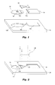
- reference 10 denotes a LED light source (including one or more LEDs) mounted on a printed circuit board (PCB) 12.
- the PCB 12 is intended to be connected with another PCB 14 carrying thereon driver electronics for the LED light source 10.
- the two PCBs 12 and 14 are provided with connection pads 12a, 14a to enable electrical connection therebetween.
- Reference 16 denotes as whole a so-called "flex" PCB (namely, a flexible PCB o FCB) carrying respective connection lines as well as pads 16a to be soldered to the pads 12a, 14a of the PCBs 10 and 14 to ensure electrical connection therebetween.
- a flexible PCB o FCB carrying respective connection lines as well as pads 16a to be soldered to the pads 12a, 14a of the PCBs 10 and 14 to ensure electrical connection therebetween.
- the pads 12a, 14a of the PCBs 12 and 14 face "upwardly" while the connection pads 16b of the flex 16 face downwardly.
- the flex 16 can thus be arranged in a bridge-like arrangement above and across the PCBs 10 and 14 while bonding (e.g. soldering) of the pads 12a, respectively 14a with the pads 16a of the flex 16.
- This result can be achieved - in a known manner - by means of a hot bar HB which is temporally superposed to the flex 16 (or at least the ends thereof) to produce soldering of the pads 12a, 14a and 16a.
- the pads 12a and 14a can be partially left uncovered by the flex allowing the direct contact between the hot bar HB and the metal pads.
- the bonding process can be also carried out by means of laser soldering techniques.
- the pads 12a and 14a may be left partially uncovered in order to allow the laser beam to reach the soldering area.
- a "flex” is a well known component adapted for connecting electrical/electronic components expected to move mutually during operation (e.g. in hard disk drives) and/or components of apparatus whose mutual positions are changed during assembly of the apparatus.
- connecting the PCBs 12, 14 via the flex involves a base plate 20.
- the metal plate 20 includes three recessed areas 120, 140 and 160.
- the recesses 120, 140 and 160 are generally “shallow” recesses having thicknesses substantially equal to the "height" or “depth” of the element intended to be received therein.
- the PCBs 12 and 14 may be arranged in the recesses 100, 140 and the flex 16 arranged in a bridge-like arrangement therebetween in such a way that the upper surface of the flex 16 lies at least approximately "flush" with the upper surface of the plate 20.
- the flex 16 (or at least the ends of the flex 16) are very precisely positioned, with the pads 16a exactly facing and abutting against the pads 12a, 14a.
- the desired bonding action may be achieved in a rapid and reliable manner by minimising the amount of the heat energy applied.
- the arrangement described herein completely dispenses with the need of using wires and/or mechanical connectors and is ideally adapted for an automated soldering process.
- the fixed shape of the flex 16 derives from the layout design, related cut and mechanical properties while the flat bonding pads (12a, 14a, 16a) provide a wide contact surface thus facilitating an automated bonding process.
- the bonding process may be automated by resorting to simple machinery (essentially a metal base properly shaped and a movable hot bar or laser soldering head).
- the layout of the flex PCB 16 can be selected to match the relative expected positions of the two PCBs 12 and 14 in the final application. Exact positioning on the three components involved in the connection process (12, 14 and 16, in the drawings herein) permits the hot bar HB (or the laser soldering beam) to move in correspondence with the pads to be soldered and apply the thermal profile required for the bonding process. Manual work is completely dispensed with in the production of lighting modules since no manual soldering is being resorted to thus giving rise to a completely automated process. No additional components are introduced by rendering the production process a very fast one. Also, the arrangement described herein lends itself to a semi-automatic implementation in the case of small volumes to be produced.
Landscapes
- Engineering & Computer Science (AREA)
- Microelectronics & Electronic Packaging (AREA)
- Combinations Of Printed Boards (AREA)
Priority Applications (3)
| Application Number | Priority Date | Filing Date | Title |
|---|---|---|---|
| EP08166750A EP2178354B1 (fr) | 2008-10-16 | 2008-10-16 | Procédé de connexion de cartes de circuits imprimés et agencement correspondant |
| US12/587,978 US8482928B2 (en) | 2008-10-16 | 2009-10-15 | Method of connecting printed circuit boards and corresponding arrangement |
| CN200910205683.3A CN101794951B (zh) | 2008-10-16 | 2009-10-16 | 连接印刷电路板的方法和相应装置 |
Applications Claiming Priority (1)
| Application Number | Priority Date | Filing Date | Title |
|---|---|---|---|
| EP08166750A EP2178354B1 (fr) | 2008-10-16 | 2008-10-16 | Procédé de connexion de cartes de circuits imprimés et agencement correspondant |
Publications (2)
| Publication Number | Publication Date |
|---|---|
| EP2178354A1 true EP2178354A1 (fr) | 2010-04-21 |
| EP2178354B1 EP2178354B1 (fr) | 2011-06-22 |
Family
ID=40452590
Family Applications (1)
| Application Number | Title | Priority Date | Filing Date |
|---|---|---|---|
| EP08166750A Not-in-force EP2178354B1 (fr) | 2008-10-16 | 2008-10-16 | Procédé de connexion de cartes de circuits imprimés et agencement correspondant |
Country Status (3)
| Country | Link |
|---|---|
| US (1) | US8482928B2 (fr) |
| EP (1) | EP2178354B1 (fr) |
| CN (1) | CN101794951B (fr) |
Cited By (1)
| Publication number | Priority date | Publication date | Assignee | Title |
|---|---|---|---|---|
| EP2623851A4 (fr) * | 2010-09-28 | 2018-04-18 | Koito Manufacturing Co., Ltd. | Module de circuit, module émetteur de lumière et lampe de véhicule |
Families Citing this family (13)
| Publication number | Priority date | Publication date | Assignee | Title |
|---|---|---|---|---|
| TWI428531B (zh) * | 2011-03-24 | 2014-03-01 | Lextar Electronics Corp | 發光模組及電源連接組件 |
| US8322906B2 (en) | 2011-08-08 | 2012-12-04 | XtraLight Manufacturing Partnership Ltd | Versatile lighting units |
| US8923003B2 (en) * | 2012-02-06 | 2014-12-30 | Apple Inc. | Flexible circuit connectors with reduced profiles |
| CN104396097B (zh) * | 2012-06-29 | 2017-04-05 | 株式会社村田制作所 | 电缆的连接、固定方法 |
| US9644829B2 (en) | 2013-04-25 | 2017-05-09 | Xtralight Manufacturing, Ltd. | Systems and methods for providing a field repairable light fixture with a housing that dissipates heat |
| US9991616B2 (en) * | 2016-03-18 | 2018-06-05 | Apple Inc. | SMT connection of rigid and flexible printed circuit boards |
| US9831579B1 (en) | 2016-08-01 | 2017-11-28 | Motorola Solutions, Inc. | Adapter frame with a set of electrical pads on its top and bottom surfaces for a board-to-board connection |
| TR201614398A2 (tr) * | 2016-10-13 | 2017-01-23 | Ttaf Elektronik Sanayi Ve Ticaret Ltd Sirketi | Chip-on-board (cob) , die-on-board (dob) veya benzer led kümeleri̇ni̇n opti̇k yapi i̇le entegre edi̇ldi̇ği̇ su geçi̇rmez aydinlatma modülü |
| TWI630862B (zh) * | 2017-03-14 | 2018-07-21 | 神雲科技股份有限公司 | 電子裝置 |
| US11139695B2 (en) | 2018-02-12 | 2021-10-05 | Ossia Inc. | Flat panel substrate with integrated antennas and wireless power transmission system |
| JP6810203B2 (ja) * | 2019-04-04 | 2021-01-06 | 台達電子企業管理(上海)有限公司 | 光源モジュール及びその製造方法 |
| US10673165B1 (en) * | 2019-07-05 | 2020-06-02 | Wbstudio Technology Media Co., Ltd. | Power connector for building blocks |
| JP6867467B1 (ja) * | 2019-12-12 | 2021-04-28 | シークス株式会社 | 電子部品実装システム及び電子部品実装方法 |
Citations (5)
| Publication number | Priority date | Publication date | Assignee | Title |
|---|---|---|---|---|
| US3579206A (en) * | 1968-12-16 | 1971-05-18 | Rca Corp | Low inductance interconnection of cryoelectric memory system |
| US5742484A (en) * | 1997-02-18 | 1998-04-21 | Motorola, Inc. | Flexible connector for circuit boards |
| US20020189862A1 (en) * | 1999-07-30 | 2002-12-19 | Toshihiro Miyake | Method for interconnecting printed circuit boards and interconnection structure |
| US6867668B1 (en) * | 2002-03-18 | 2005-03-15 | Applied Micro Circuits Corporation | High frequency signal transmission from the surface of a circuit substrate to a flexible interconnect cable |
| US20070040626A1 (en) * | 2002-03-18 | 2007-02-22 | Applied Micro Circuits Corporation | Flexible interconnect cable with coplanar waveguide |
Family Cites Families (6)
| Publication number | Priority date | Publication date | Assignee | Title |
|---|---|---|---|---|
| US5422900A (en) * | 1994-04-28 | 1995-06-06 | Eastman Kodak Company | Integrated laser module |
| US5777855A (en) * | 1996-06-18 | 1998-07-07 | Eastman Kodak Company | Method and apparatus for connecting flexible circuits to printed circuit boards |
| CN101048041B (zh) * | 2006-03-30 | 2011-01-26 | 光宝科技股份有限公司 | 接合柔性印刷电路板与柔性电路组件的方法及相关结构 |
| TW200802956A (en) * | 2006-06-16 | 2008-01-01 | Gigno Technology Co Ltd | Light emitting diode module |
| CN101408291A (zh) * | 2007-10-11 | 2009-04-15 | 富士迈半导体精密工业(上海)有限公司 | 光源模组及相应的光源装置 |
| US7944708B2 (en) * | 2008-03-28 | 2011-05-17 | Chi-Hsin Lin | Structured light-emitting module for lighting apparatus |
-
2008
- 2008-10-16 EP EP08166750A patent/EP2178354B1/fr not_active Not-in-force
-
2009
- 2009-10-15 US US12/587,978 patent/US8482928B2/en not_active Expired - Fee Related
- 2009-10-16 CN CN200910205683.3A patent/CN101794951B/zh not_active Expired - Fee Related
Patent Citations (5)
| Publication number | Priority date | Publication date | Assignee | Title |
|---|---|---|---|---|
| US3579206A (en) * | 1968-12-16 | 1971-05-18 | Rca Corp | Low inductance interconnection of cryoelectric memory system |
| US5742484A (en) * | 1997-02-18 | 1998-04-21 | Motorola, Inc. | Flexible connector for circuit boards |
| US20020189862A1 (en) * | 1999-07-30 | 2002-12-19 | Toshihiro Miyake | Method for interconnecting printed circuit boards and interconnection structure |
| US6867668B1 (en) * | 2002-03-18 | 2005-03-15 | Applied Micro Circuits Corporation | High frequency signal transmission from the surface of a circuit substrate to a flexible interconnect cable |
| US20070040626A1 (en) * | 2002-03-18 | 2007-02-22 | Applied Micro Circuits Corporation | Flexible interconnect cable with coplanar waveguide |
Cited By (1)
| Publication number | Priority date | Publication date | Assignee | Title |
|---|---|---|---|---|
| EP2623851A4 (fr) * | 2010-09-28 | 2018-04-18 | Koito Manufacturing Co., Ltd. | Module de circuit, module émetteur de lumière et lampe de véhicule |
Also Published As
| Publication number | Publication date |
|---|---|
| US20100099276A1 (en) | 2010-04-22 |
| US8482928B2 (en) | 2013-07-09 |
| EP2178354B1 (fr) | 2011-06-22 |
| CN101794951B (zh) | 2014-02-19 |
| CN101794951A (zh) | 2010-08-04 |
Similar Documents
| Publication | Publication Date | Title |
|---|---|---|
| EP2178354B1 (fr) | Procédé de connexion de cartes de circuits imprimés et agencement correspondant | |
| US10247378B2 (en) | Metal PCB, headlight module having metal PCB applied thereto, and method for assembling headlight module | |
| US10337687B2 (en) | Metal PCB assembly for vehicle lamp and manufacturing method thereof | |
| CN103460813B (zh) | 用于安装多个发光元件的基板 | |
| CN100543983C (zh) | 在基底表面上制造电路板层的方法 | |
| US10548231B2 (en) | Apparatus for depositing conductive and nonconductive material to form a printed circuit | |
| JP2016139514A (ja) | 給電アタッチメント、光源モジュールおよび車両用灯具 | |
| US9756730B2 (en) | Chip-integrated through-plating of multi-layer substrates | |
| KR20170084800A (ko) | 차량램프용 메탈 pcb 조립체 및 그 조립방법 | |
| EP3847395B1 (fr) | Dispositif d'éclairage comprend une carte de circuit imprimé | |
| TWI278702B (en) | Light source module and panel shape light source device | |
| KR101436210B1 (ko) | 차량용 등기구 | |
| CN105590636A (zh) | 配线电路基板和其制造方法以及配线电路基板组件和其制造方法 | |
| US7567313B2 (en) | Bezel design for surface mount display modules | |
| KR101652963B1 (ko) | 다방향 메탈 피시비 조립방법 | |
| US11480328B2 (en) | LED lamp having metal PCB bent polyhedrally and manufacturing method thereof | |
| JP2003249738A (ja) | プリント基板、電子部品の実装構造及び光ピックアップ | |
| KR101065505B1 (ko) | 용착기, 다층프린트 배선판의 제조방법 | |
| JP7012413B2 (ja) | 照明装置及び該照明装置の製造方法 | |
| KR102630908B1 (ko) | 방열성능이 향상되는 메탈피시비 | |
| CN101313172A (zh) | 发光模块和制造方法 | |
| CN108603645A (zh) | 用于机动车的照明装置的光模块的保持装置的加工方法 | |
| JP6141357B2 (ja) | 口金及び照明ランプ | |
| KR20240080787A (ko) | 홀 드릴링 패턴을 이용한 접합소재 레이저 솔더링 접합방법 및 이에 사용되는 접합물 구조체 | |
| JP2008192925A (ja) | 基板モジュール |
Legal Events
| Date | Code | Title | Description |
|---|---|---|---|
| PUAI | Public reference made under article 153(3) epc to a published international application that has entered the european phase |
Free format text: ORIGINAL CODE: 0009012 |
|
| AK | Designated contracting states |
Kind code of ref document: A1 Designated state(s): AT BE BG CH CY CZ DE DK EE ES FI FR GB GR HR HU IE IS IT LI LT LU LV MC MT NL NO PL PT RO SE SI SK TR |
|
| AX | Request for extension of the european patent |
Extension state: AL BA MK RS |
|
| RAP1 | Party data changed (applicant data changed or rights of an application transferred) |
Owner name: OSRAM S.P.A. - SOCIETA' RIUNITE OSRAM EDISON CLERI Owner name: OSRAM GESELLSCHAFT MIT BESCHRAENKTER HAFTUNG |
|
| 17P | Request for examination filed |
Effective date: 20100913 |
|
| 17Q | First examination report despatched |
Effective date: 20101006 |
|
| AKX | Designation fees paid |
Designated state(s): DE FR GB IT |
|
| GRAP | Despatch of communication of intention to grant a patent |
Free format text: ORIGINAL CODE: EPIDOSNIGR1 |
|
| GRAS | Grant fee paid |
Free format text: ORIGINAL CODE: EPIDOSNIGR3 |
|
| GRAA | (expected) grant |
Free format text: ORIGINAL CODE: 0009210 |
|
| AK | Designated contracting states |
Kind code of ref document: B1 Designated state(s): DE FR GB IT |
|
| REG | Reference to a national code |
Ref country code: GB Ref legal event code: FG4D |
|
| REG | Reference to a national code |
Ref country code: DE Ref legal event code: R096 Ref document number: 602008007757 Country of ref document: DE Effective date: 20110804 |
|
| RAP2 | Party data changed (patent owner data changed or rights of a patent transferred) |
Owner name: OSRAM AG Owner name: OSRAM S.P.A. - SOCIETA' RIUNITE OSRAM EDISON CLERI |
|
| PLBE | No opposition filed within time limit |
Free format text: ORIGINAL CODE: 0009261 |
|
| STAA | Information on the status of an ep patent application or granted ep patent |
Free format text: STATUS: NO OPPOSITION FILED WITHIN TIME LIMIT |
|
| 26N | No opposition filed |
Effective date: 20120323 |
|
| REG | Reference to a national code |
Ref country code: DE Ref legal event code: R097 Ref document number: 602008007757 Country of ref document: DE Effective date: 20120323 |
|
| REG | Reference to a national code |
Ref country code: FR Ref legal event code: PLFP Year of fee payment: 8 |
|
| PGFP | Annual fee paid to national office [announced via postgrant information from national office to epo] |
Ref country code: GB Payment date: 20151021 Year of fee payment: 8 Ref country code: IT Payment date: 20151028 Year of fee payment: 8 |
|
| PGFP | Annual fee paid to national office [announced via postgrant information from national office to epo] |
Ref country code: FR Payment date: 20151023 Year of fee payment: 8 |
|
| GBPC | Gb: european patent ceased through non-payment of renewal fee |
Effective date: 20161016 |
|
| REG | Reference to a national code |
Ref country code: FR Ref legal event code: ST Effective date: 20170630 |
|
| PG25 | Lapsed in a contracting state [announced via postgrant information from national office to epo] |
Ref country code: FR Free format text: LAPSE BECAUSE OF NON-PAYMENT OF DUE FEES Effective date: 20161102 Ref country code: GB Free format text: LAPSE BECAUSE OF NON-PAYMENT OF DUE FEES Effective date: 20161016 |
|
| PG25 | Lapsed in a contracting state [announced via postgrant information from national office to epo] |
Ref country code: IT Free format text: LAPSE BECAUSE OF NON-PAYMENT OF DUE FEES Effective date: 20161016 |
|
| PGFP | Annual fee paid to national office [announced via postgrant information from national office to epo] |
Ref country code: DE Payment date: 20171019 Year of fee payment: 10 |
|
| REG | Reference to a national code |
Ref country code: DE Ref legal event code: R119 Ref document number: 602008007757 Country of ref document: DE |
|
| PG25 | Lapsed in a contracting state [announced via postgrant information from national office to epo] |
Ref country code: DE Free format text: LAPSE BECAUSE OF NON-PAYMENT OF DUE FEES Effective date: 20190501 |