EP2178599B1 - Procédé et système pour couplage de signaux et blocage de courant continu - Google Patents
Procédé et système pour couplage de signaux et blocage de courant continu Download PDFInfo
- Publication number
- EP2178599B1 EP2178599B1 EP08772071A EP08772071A EP2178599B1 EP 2178599 B1 EP2178599 B1 EP 2178599B1 EP 08772071 A EP08772071 A EP 08772071A EP 08772071 A EP08772071 A EP 08772071A EP 2178599 B1 EP2178599 B1 EP 2178599B1
- Authority
- EP
- European Patent Office
- Prior art keywords
- double
- signal
- capacitive element
- circuit
- coupling
- Prior art date
- Legal status (The legal status is an assumption and is not a legal conclusion. Google has not performed a legal analysis and makes no representation as to the accuracy of the status listed.)
- Active
Links
Images


Classifications
-
- A—HUMAN NECESSITIES
- A61—MEDICAL OR VETERINARY SCIENCE; HYGIENE
- A61N—ELECTROTHERAPY; MAGNETOTHERAPY; RADIATION THERAPY; ULTRASOUND THERAPY
- A61N1/00—Electrotherapy; Circuits therefor
- A61N1/18—Applying electric currents by contact electrodes
- A61N1/32—Applying electric currents by contact electrodes alternating or intermittent currents
-
- H—ELECTRICITY
- H01—ELECTRIC ELEMENTS
- H01G—CAPACITORS; CAPACITORS, RECTIFIERS, DETECTORS, SWITCHING DEVICES, LIGHT-SENSITIVE OR TEMPERATURE-SENSITIVE DEVICES OF THE ELECTROLYTIC TYPE
- H01G11/00—Hybrid capacitors, i.e. capacitors having different positive and negative electrodes; Electric double-layer [EDL] capacitors; Processes for the manufacture thereof or of parts thereof
- H01G11/08—Structural combinations, e.g. assembly or connection, of hybrid or EDL capacitors with other electric components, at least one hybrid or EDL capacitor being the main component
-
- H—ELECTRICITY
- H01—ELECTRIC ELEMENTS
- H01G—CAPACITORS; CAPACITORS, RECTIFIERS, DETECTORS, SWITCHING DEVICES, LIGHT-SENSITIVE OR TEMPERATURE-SENSITIVE DEVICES OF THE ELECTROLYTIC TYPE
- H01G11/00—Hybrid capacitors, i.e. capacitors having different positive and negative electrodes; Electric double-layer [EDL] capacitors; Processes for the manufacture thereof or of parts thereof
- H01G11/78—Cases; Housings; Encapsulations; Mountings
- H01G11/82—Fixing or assembling a capacitive element in a housing, e.g. mounting electrodes, current collectors or terminals in containers or encapsulations
-
- H—ELECTRICITY
- H04—ELECTRIC COMMUNICATION TECHNIQUE
- H04B—TRANSMISSION
- H04B3/00—Line transmission systems
- H04B3/54—Systems for transmission via power distribution lines
- H04B3/56—Circuits for coupling, blocking, or by-passing of signals
-
- H—ELECTRICITY
- H04—ELECTRIC COMMUNICATION TECHNIQUE
- H04B—TRANSMISSION
- H04B5/00—Near-field transmission systems, e.g. inductive or capacitive transmission systems
- H04B5/20—Near-field transmission systems, e.g. inductive or capacitive transmission systems characterised by the transmission technique; characterised by the transmission medium
- H04B5/22—Capacitive coupling
-
- A—HUMAN NECESSITIES
- A61—MEDICAL OR VETERINARY SCIENCE; HYGIENE
- A61N—ELECTROTHERAPY; MAGNETOTHERAPY; RADIATION THERAPY; ULTRASOUND THERAPY
- A61N1/00—Electrotherapy; Circuits therefor
- A61N1/40—Applying electric fields by inductive or capacitive coupling ; Applying radio-frequency signals
-
- H—ELECTRICITY
- H04—ELECTRIC COMMUNICATION TECHNIQUE
- H04B—TRANSMISSION
- H04B2203/00—Indexing scheme relating to line transmission systems
- H04B2203/54—Aspects of powerline communications not already covered by H04B3/54 and its subgroups
- H04B2203/5462—Systems for power line communications
- H04B2203/5483—Systems for power line communications using coupling circuits
-
- Y—GENERAL TAGGING OF NEW TECHNOLOGICAL DEVELOPMENTS; GENERAL TAGGING OF CROSS-SECTIONAL TECHNOLOGIES SPANNING OVER SEVERAL SECTIONS OF THE IPC; TECHNICAL SUBJECTS COVERED BY FORMER USPC CROSS-REFERENCE ART COLLECTIONS [XRACs] AND DIGESTS
- Y02—TECHNOLOGIES OR APPLICATIONS FOR MITIGATION OR ADAPTATION AGAINST CLIMATE CHANGE
- Y02E—REDUCTION OF GREENHOUSE GAS [GHG] EMISSIONS, RELATED TO ENERGY GENERATION, TRANSMISSION OR DISTRIBUTION
- Y02E60/00—Enabling technologies; Technologies with a potential or indirect contribution to GHG emissions mitigation
- Y02E60/13—Energy storage using capacitors
Definitions
- the present invention relates to a signal coupling method and class of circuit configurations.
- the present invention relates to a method and system of signal coupling by replacing conventional film type or ceramic monolithic coupling capacitors in otherwise conventional coupling circuits with symmetrical carbon double-layer capacitors.
- ⁇ is conveniently expressed as the product of ⁇ 0 times ⁇ R , where ⁇ R is a dimensionless number characteristic of the material.
- ⁇ R typically ranges from about 2 for perfluorinated hydrocarbons such as Teflon ® , through values of 3 to 6 typical of most plastics and minerals, 8.8 for aluminum oxide, 30 for tantalum oxide and 80 for distilled water, up to about 1200 for specially processed forms of barium titanate.
- capacitance may be increased either by increasing S, by increasing e, or by decreasing d.
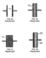
- Early capacitors using empty space (or more practically, air) between their plates, as indicated by 30 in Figure 2a had very small values of C, on the order of a few picofarads (10 -12 farad) up to a few hundred picofarads. While useful at very high frequencies or at voltages up to many thousand volts, such capacitors find little use in other modern low-voltage electronics.
- ferroelectric ceramics most of them based on specially processed barium titanate made possible a further generation of capacitors termed monolithic.
- Such a "chip” capacitor is built up from alternating thin (about 10 -4 meter) layers of ceramic 34 and a metal such as palladium, fired together into a single ceramic piece, as illustrated in Figure 2c . While practical devices are small, they are easier to manufacture than film capacitors and much more durable.
- the very high value of ⁇ R in ceramic 34 typically around 1200, offsets the necessarily reduced S yielding practical values from a few nanofarads to about one microfarad (10 -6 farad) with working voltages typically of ten to thirty volts.
- Ferroelectric ceramics may also be used in "disk” capacitors where the ceramic replaces material 32 in the previous example, yielding smaller values of capacitance but able to operate at higher voltages.
- the electrolytic capacitor as illustrated in Figure 2d .
- at least one plate is formed of a metal such as aluminum or tantalum, etched or otherwise processed to maximize its surface area, then placed in contact with an electrolyte 36.
- a thin (10 -6 meter or so) layer of oxide 38 is grown on the surface and forms the dielectric.
- ⁇ R is moderately high (though not as high as in a ferroelectric ceramic) and d is orders of magnitude thinner than would be possible in a mechanically built-up structure, capacitance values from one microfarad (10 -6 farad) to many thousand microfarads are easily achieved at working voltages ranging from a few volts to a few hundred volts.
- Electrolytics revolutionized electronics by making relatively large capacitance values economically achievable. Electrolytics have a downside, however, in that they are inherently unidirectional or polarized. This results from the manufacturing process and the chemistry of the metal and electrolyte. So long as the applied voltage has the same polarity of that used to form the oxide layer originally, the capacitor functions as intended. If the voltage is reversed, however, the oxide layer breaks down and the capacitor becomes extremely leaky resulting essentially in a short circuit. This requires special precautions in the use of electrolytic capacitors, limiting their usefulness to applications such as power storage in which the applied voltage is always of the same, correct polarity.
- this layer is very thin, often less than a nanometer (10 -9 meter), and because the surface area S of a body of activated carbon or carbon aerogel is extremely high, practical capacitance values in devices of this sort range from a minimum of about 0.05 farad (50,000 microfarads) upward to many farads.
- the downside arises from this same thinness: a single capacitor of this type is limited, depending on its construction and the liquid forming the dielectric, to a maximum working voltage of no more than two or three volts. For higher voltages, multiple units must be connected in series.
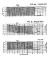
- Figure 3 illustrates the self-discharge curves measured for a typical ELNA DX-5R5V473 "Dynacap” (0.047 farad, 5.5 volts) capacitor 48 in both the marked “forward” and marked “reverse” directions.
- the capacitor 48 was charged from a 9-volt alkaline radio battery through a 100-ohm resistor until a connected voltmeter read 8.50 volts, well above the rated Dynacap maximum working voltage of 5.5 volts, indicated by line 60 in Figure 3a . The battery was then disconnected. The capacitor voltage was measured at increasing intervals and plotted against the logarithm of time. Smooth curves 62 and 64 were then fitted to the nominal "forward” and “reverse” data points respectively as illustrated in Figure 3a .
- capacitive coupling is the transfer of electrical energy from one circuit element to another circuit element using the capacitance between the circuit elements.
- Capacitive coupling is typically achieved by placing a capacitor in series with the signal to be coupled. Such a capacitor may be called a coupling capacitor.
- a coupling capacitor is used to connect two circuits such that only the alternating current (AC) signal from the first circuit can pass through to the next while direct current (DC) is blocked. This technique may be used to avoid altering the DC bias settings of each circuit when they are interconnected.
- capacitive coupling is also known as AC coupling.
- a coupling capacitor may be known as a DC blocking capacitor.
- Capacitive coupling has the disadvantage of degrading the low frequency performance of a system containing capacitively coupled units, since each coupling capacitor along with the input impedance of the next stage forms a highpass filter and each successive filter results in a cumulative filter.
- the coupling capacitor usually must have high enough capacitance so that the reactance (at the lowest frequency of interest) is much higher than the input impedance of the next stage. Poor low-frequency performance of a coupling capacitor can complicate the transfer of A/C electrical signal having long time constants.
- a method and class of circuit configurations are described for coupling low-frequency signals from one stage of an electronic apparatus to another stage, from the outside world to such a stage, or from such a stage to the outside world, through the use of one or more double-layer capacitors.
- the double-layer capacitors can be combined with other, readily available and low-cost electronic components used in electronic circuit design, such as resistors.
- One important feature of the invention is the use of compact, economical symmetrical double-layer capacitors for signal transmission, as distinguished from energy storage.
- the method may be beneficial for introducing signals from electronic apparatus into biological materials, such as the living human or animal body, other organisms, or cells or tissues in culture.
- double-layer capacitors providing higher values of capacitance in devices of practically small size and cost, can permit the transmission of a potentially much wider range of signals with far less distortion while still blocking any significant direct current.
- the double-layer capacitors can be connected in the path of signal flow with both capacitor terminals floating, rather than as usual with double-layer capacitors having at least one terminal connected to ground or another point of fixed voltage. This permits the passage of alternating- current components of a signal through the capacitors from one stage of an electronic apparatus to another stage, from the outside world to such a stage, or from such a stage to the outside world, while blocking any direct current component.
- This feature can be important especially in bioelectronic stimulators and similar medical devices, in which any net direct current applied to living tissue can cause harmful electrolytic reactions.
- Another important feature of the invention is the use of multiple, discrete double-layer capacitor devices connected in series, regardless of whether each such device comprises a single cell or a stack of two or more, while maintaining adequate capacitance for successful coupling. For example, two such devices could be connected in series.
- double-layer capacitors can be used in the same way as other nonpolarized capacitors yet with exceptionally extended timing characteristics due to their orders-of-magnitude higher values.
- capacitors can be used to couple exceptionally low-frequency alternating current (A/C) signals, such as on the order of 20 Hz or less at ordinary impedance levels, or low audio frequencies in the 100 Hz range when unusually low impedances are used or when distortion must be minimized for some medical applications.
- A/C alternating current
- Other low frequencies can include, but are not limited to, a 5-15 Hz band, as well as 0.00056 Hz (reversing every 15 minutes, full cycle every 30, - which signal generation technique is often referred to as the Borgens application for nerve regrowth), and frequencies as low as 0.0001 Hz.
- Additional low frequencies can include, but are not limited to, one Hertz (Hz), one-tenth, three tenths, one hundredth, three hundredths, one thousandth, three thousandths, one ten-thousandth, and three ten thousandths of a Hertz.
- Hz Hertz
- other low frequencies are not beyond the scope of the invention.
- the capacitors can couple these low frequency A/C signals from one stage of an electronic apparatus to another stage, from the outside world to such a stage, or from such a stage to the outside world, while still blocking any direct-current components of such signals and without the need to ensure a specific, unchanging polarity exists across the capacitor.
- this field of applications includes the coupling of low-frequency signals between electronic apparatus and the human or animal body, cells, tissues or complete organisms in culture for purposes of diagnosis, treatment, the acceleration of growth or healing, or other purposes in the art of electrobiology and electrostimulation without the accompanying risk of electrolytic effects from prolonged exposure to signals which may inadvertently contain some direct current component.
- Yet another important feature of the invention is the use of double-layer capacitors along with relatively low-valued resistors to match the impedances of typical biological materials while maintaining long time constants, such as on the order of seven, sixteen, thirty-six, one hundred twenty, one hundred fifty, five hundred, twelve hundred, and fifteen hundred seconds, just to name a few examples.
- long time constants can include, but are not limited to, ones on the order of ten, thirty, one hundred, three hundred, one thousand, three thousand, or potentially as long as ten thousand seconds.
- R 1 , R2, R3, etc. and C1, C2, C3, etc. are resistances and capacitances all connected in series.
- the resulting coupling circuits permit the economical achievement of exceptionally long time constants (on the order of on the order of ten, thirty, one hundred, three hundred, one thousand, three thousand or potentially as long as ten thousand seconds) and large charge displacements (on the order of 0.25 coulomb) and thus the coupling of exceptionally low frequencies or signals containing such low-frequency components, especially those below 20Hz, for example into biological materials for purposes of diagnosis, treatment or the acceleration of growth or healing while still blocking any direct current component of the signals.
- the invention includes a method and class of circuit configurations for coupling low-frequency signals from one stage of an electronic apparatus to another stage, from the outside world to such a stage, or from such a stage to the outside world, through the use of one or more preferably a plurality of double-layer capacitors, combined with other, readily available and low-cost electronic components such as resistors.
- the double-layer capacitors can be connected in the path of signal flow with both capacitor terminals floating, contrary to the conventional usage of double-layer capacitors where at least one terminal is connected to ground or some other fixed voltage potential.
- the invention can be applied to the field of bioelectronic stimulation, in which a signal of specific strength and waveform is applied to a biological material to elicit a desired response such as the acceleration of growth or healing.
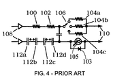
- resistors 104a, 104b and 104c there are three redundant resistors in series that include 100, 102, and one that is selected from a group of resistors 104a, 104b and 104c as determined by the position of switch 106. Values of these resistors are calculated so that, if any one of them should fail as a short circuit, the remaining two, together with other distributed resistances in drivers 108 and elsewhere in the circuit, will suffice to limit currents at output terminals 110 to safe levels. Resistors alone, however, cannot by themselves distinguish an alternating current from a direct current signal and thus cannot ensure that the signal at terminals 110 is charge-balanced (i.e., has no D.C. component) as is also required for safe use.
- Diodes 103 and 105 are not essential to circuit operation, but provide a visual or electronic indication that current is flowing. At least one of these diodes, shown in the figure as 105, is a light-emitting diode (LED) which may be either a visible LED, or the infrared LED in an optical isolator providing electronic input, for example, to a microprocessor. Alternatively, both diodes 103 and 105 may be LEDs. With the diodes arranged in an antiparallel (non-parallel) manner as shown (in which the anode of each is tied to the cathode of the other), the pair is able to pass a high-frequency signal and emit light in proportion to the current flowing. This provides an indication simultaneously that the battery is providing adequate operating voltage, that all circuit blocks which it powers are functioning correctly, and that current is properly flowing to the load connected at terminal 110.
- LED light-emitting diode
- capacitors 112a, 112b, 112c and 112d are also in Figure 4 , so that if any one of them fails the other unit which is connected in the same polarity can still suffice to block direct current from the output and thus ensure safe operation.
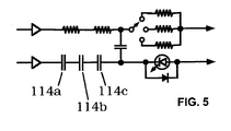
- FIG 5 the same output coupling section of Figure 4 is shown redrawn using double-layer capacitors according to the present invention. At least three such capacitors 114a, 114b and 114c are used, thus satisfying the "rule of three.” Unit working voltages are chosen so that in the event of failure of any capacitor as a short circuit, the remaining units together will still safely block any direct current signal component without exceeding their rated voltages. For example, with a 9-volt maximum applied signal, three 5.5-volt double-layer capacitors such as those in the ELNA DX series of capacitors may be used, any two sufficing for safe operation.
- each device has a capacitance of 0.047 farad and thus the string of three has a series capacitance of about 0.0157 farad: 15,700 microfarads, or more than 6000 times that of the equivalent string in Figure 4 .
- the resulting time constant is 7.83 seconds. Still longer time constants are readily achievable using other devices from the same series or from others like it having standard, 10% tolerance stock values as indicated in Table 1.
- longer time constants can include, but are not limited to, ones on the order of seven, sixteen, thirty-six, one hundred twenty, one hundred fifty, five hundred, twelve hundred, and fifteen hundred seconds (as shown in Table 1), just to name a few examples.
- Other values for long time constants can include, but are not limited to, ones on the order of ten, thirty, one hundred, three hundred, one thousand, three thousand, or potentially as long as ten thousand seconds. Therefore, some time constants supported by the invention can range from between ten to ten-thousand seconds and, other ranges, such as between one hundred and one-thousand seconds.
- Additional low frequencies can include, but are not limited to, one Hertz (Hz), one-tenth, three tenths, one hundredth, three hundredths, one thousandth, three thousandths, one ten-thousandth, and three ten thousandths of a Hertz.
- Hz Hertz
- other low frequencies are not beyond the scope of the invention.
- Table 1 - Capacitor Values and related Time Constants Single capacitor value (farads) Value of three capacitors in series (farads) Time constant with 500 ohms in series (seconds) 0.047 0.0157 7.83 0.10 0.0333 16.7 0.22 0.0733 36.7 0.33 0.110 50 1.0 0.333 150 (2.5 minutes) 3.3 1.10 500 (8.33 minutes) 10 3.33 1500 (25 minutes)
- Low frequencies produced by the invention can include, but are not limited to, a 5-15 Hz band, as well as 0.00056 Hz (reversing every 15 minutes, full cycle every 30, - which signal generation technique is often referred to as the Borgens application for nerve regrowth), and frequencies as low as 0.0001 Hz. Additional low frequencies can include, but are not limited to, one Hertz (Hz), one-tenth, three tenths, one hundredth, three hundredths, one thousandth, three thousandths, one ten-thousandth, and three ten thousandths of a Hertz. However, other low frequencies are not beyond the scope of the invention. However, other low frequencies are not beyond the scope of the invention.
- Figure 6 illustrates and compares the signal coupling characteristics of the prior art output section in Figure 4 with that in Figure 5 embodying the invention.
- Trace 120 of Figure 6a shows the differential output voltage from drivers 108.
- the signal takes the form of a train 122 of short, asymmetric pulses, followed by an equalizing pulse 124 which, since made approximately equal to the difference between times spent at positive and negative polarities within train 122, restores electrical balance for zero net charge (no D.C. content). Since with practical components it cannot be assured that no failure or value change will affect this balance, however, capacitive D.C. blocking is still required for safety. Desirably, the same voltage pattern in trace 120 would be reproduced almost unchanged across the biological material being treated.
- Trace 126 of Figure 6b of the prior art shows the signal from the output section appearing across a 500 ohm resistance, representing a typical biological load, placed between terminals 110.
- the distortion introduced by the combination of capacitors 112a through 112d is clearly seen in the form of voltage droop along the length of train 122, resulting in positive pulses diminishing in strength over time while the negative pulses increase in strength. All pulses are noticeably distorted in shape as well, with equalizing pulse 124 dramatically so.
- Trace 128 of Figure 6c of one embodiment of the invention shows the same signal when capacitors 122a through 122d have been replaced with three double-layer capacitors 124a through 124c as detailed above. As can be seen, there is no detectable distortion between the applied voltage and that appearing across the load.
- Figure 7 illustrates a double layer capacitor 46 coupling a signal 710 between a first circuit 700a and a second circuit 700b according to one exemplary embodiment of the invention.
- the conductors 20a and 20b operate to interconnect the first circuit 700a to the coupling capacitors 46 and the coupling capacitors to the second circuit 700b.
- This interconnection provides a conductive pathway for alternating current (A/C) electrical signals 710 from one circuit to the other through the double layer capacitors 46.
- A/C alternating current
- the capacitor 46 may substantially block the direct current (D.C.) components of any signals 710 that it couples between the first circuit 700a and the second circuit 700b. However, the capacitor 46 can couple a substantial portion of the other low frequency energy contained within A/C signals 710 that the capacitor 46 operates to couple between the first circuit 700a and the second circuit 700b.
- D.C. direct current
- the double layer capacitors can comprise any capacitor exhibiting symmetrical double layer characteristics, for example a two sided carbon super capacitor 46 as illustrated.
- each capacitor shown may be replaced with two identical, asymmetrical supercapacitors in a back-to-back configuration analogous to that of a capacitor pair as illustrated in Figure 4 .
- such a capacitor can achieve the desired double layer when one layer is formed by mobile electrons in the carbon 42 and the other by mobile ions in the electrolyte 36.
- a voltage of the correct polarity applied across this double layer draws the opposite charges apart, leaving a thin empty zone which forms the dielectric of the capacitor.
- the dielectric is based on the surface barrier potential which arises at any junction between a semiconductor such as carbon and another material.
- the double layer capacitor can also comprise a stacked capacitor 48 as discussed with respect to Figure 2h . Multiple capacitors placed in series may also be used as shown in Figure 8a.
- the capacitors illustrated in Figure 8a may each be dual layer capacitor units 46 as shown or each may be stacked double layer capacitors cells 48 having two, three, or more than three cells per stacked capacitor 48 (See Figure 2h ).
- Series, and/or stacked, capacitors can provide for redundancy in the signal path, protecting the load from the failure of one or more of the individual capacitors 46.
- An example of such redundancy is the "rule of three" as discussed above.
- the circuit 700a can be coupled to dual layer capacitor units 46 which are coupled to biological material.
- the biological material can comprise a living organism.
- the living organism can comprise tissue, cells in culture, a living human body, a living animal other than human, and other like living organisms.
- capacitors illustrated in Figures 7 and 8 are illustrated as parallel plate 12a and 12b capacitors, they may have any other geometry or electrochemical make-up known in the art to achieve a double-layer, super capacitor, or ultracapacitor effect. Examples of other geometries may be wrapped coils, concentric plates, stacked plates, radially interleaved plates, plates with surfaces treated or textured to increase surface area.
- Materials within the capacitors 46 may include any combination of carbon, silicon, geranium, gallium arsenide, doped semiconductors, combinations thereof, or any other semiconductor; electrolytic liquids, gases, electrolytic gells, electrolytic pastes, electrolytic solids, electrolytic matrix, or any such electrolytic materials; and metal or oxide layers such as copper, nickel, aluminum, alloys, any other conductors, metal oxides, silicon oxides, or any alloys or combinations thereof, as examples.
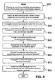
- FIG. 9 this figure illustrates a logical flow diagram 900 of a process for coupling an A/C electrical signal between a circuit and a component using a double layer capacitor according to one exemplary embodiment of the present invention.
- the component can comprise another circuit or biological material.
- the method 900 using double-layer capacitors to couple an A/C electrical signal between a circuit and a component can begin with Step 910 where an A/C electrical signal 710 from a first circuit 700a is supplied into a first conductor 20a.
- Step 920 the A/C electrical signal 710 is propagated along the first conductor 20a.
- This conductor may be in electrical communication between the first circuit 700a and the double-layer coupling capacitor 46.
- the A/C electrical signal 710 is conducted from the first conductor 700a into a double-layer capacitor 46.
- This capacitor 46 is used here as a coupling capacitor.
- the double-layer capacitor 46 may be a solitary capacitor cell demonstrating double capacitor characteristics, or it may be a series connection of one or more of such capacitors, or it may be one or more stacked capacitors 48.
- Such double layer capacitors may be also be known as super capacitors or ultracapacitors.
- Step 940 the A/C electrical signal 710 is coupled through the double layer capacitor 46. Coupling the A/C electrical signal through the double layer capacitor 46 may be considered as the propagation of the alternating current components of the A/C electrical signal 710.
- Step 950 any direct current (D.C.) components of the A/C electrical signal 710 are substantially blocked from being coupled through the capacitor 46.
- Step 960 the A/C electrical signal is conducted from the double-layer capacitor 46 into a second conductor 20b.
- the second conductor 20b can be in electrical communication with the second plate 12b of the capacitor 46.
- Step 970 the A/C electrical signal 710 is propagated along the second conductor 20b.
- Step 980 the A/C electrical signal 710 is delivered from the second conductor 20b into a component such as second circuit 700b of Figure 8 or a component such a biological material.
- the delivered signal should be substantially similar to the signal originally supplied in Step 910, however, any direct current (D.C.) components will have been substantially blocked by the double-layer capacitor 46.
- the delivery of the A/C signal may demonstrate excellent low-frequency performance and thereby be beneficial for conducting signals 710 with long time-constant components.
- time constants supported by the invention can include, but are not limited to, ones on the order of seven, sixteen, thirty-six, one hundred twenty, one hundred fifty, five hundred, twelve hundred, and fifteen hundred seconds, just to name a few examples. Therefore, some time constants supported by the invention can range from between five to seventy-two hundred seconds and, other ranges, such as between one hundred fifty and twelve hundred seconds.
- Low-frequency A/C signals supported by the invention can include, but are not limited to, signals with frequencies such as on the order between 20 Hz. and 0.0001 Hz.
- This step of coupling the A/C electrical signal through the double layer capacitor 46 may couple low frequency components of the A/C electrical signal 710 more effectively than a single-layer capacitor 30 couples the low frequency components of the A/C electrical signal 710.
Landscapes
- Engineering & Computer Science (AREA)
- Power Engineering (AREA)
- Health & Medical Sciences (AREA)
- Microelectronics & Electronic Packaging (AREA)
- Signal Processing (AREA)
- Computer Networks & Wireless Communication (AREA)
- Radiology & Medical Imaging (AREA)
- General Health & Medical Sciences (AREA)
- Public Health (AREA)
- Veterinary Medicine (AREA)
- Animal Behavior & Ethology (AREA)
- Life Sciences & Earth Sciences (AREA)
- Nuclear Medicine, Radiotherapy & Molecular Imaging (AREA)
- Biomedical Technology (AREA)
- Electrotherapy Devices (AREA)
- Electric Double-Layer Capacitors Or The Like (AREA)
- Filters And Equalizers (AREA)
- Cable Transmission Systems, Equalization Of Radio And Reduction Of Echo (AREA)
Claims (12)
- Circuit de couplage, comprenant :un premier conducteur (20a) en communication électrique avec un premier circuit externe (700a) ;un second conducteur (20b) en communication électrique avec un second circuit externe (700b) ;un élément capacitif à double couche (46, 48) entre le premier conducteur et le second conducteur et couplant un signal électrique à courant alternatif (CA) entre le premier circuit externe et le second circuit externe, l'élément capacitif à double couche étant en outre utilisable pour bloquer sensiblement un composant courant continu (CC) du signal électrique CA ; etune résistance (104a-104c) en communication avec l'élément capacitif à double couche, la résistance étant utilisable pour améliorer l'adaptation d'impédance entre le premier circuit externe et le second circuit externe.
- Circuit de couplage selon la revendication 1, dans lequel l'élément capacitif à double couche comprend au moins un parmi :a) un semi-conducteur en contact avec un matériau électrolytique ;b) un premier semi-conducteur en contact avec un matériau électrolytique, et un second semi-conducteur en contact avec le matériau électrolytique ;c) une pluralité de condensateurs à double couche connectés en série ; oud) un ou plusieurs ultracondensateurs.
- Circuit de couplage selon la revendication 1, dans lequel le signal électrique CA comprend une charge non équilibrée.
- Circuit de couplage selon la revendication 1, comprenant en outre une résistance en communication avec l'élément capacitif à double couche, la résistance étant utilisable pour améliorer l'adaptation d'impédance entre le premier circuit externe et le second circuit externe.
- Circuit de couplage selon la revendication 1, comprenant en outre une résistance, la résistance et l'élément capacitif à double couche étant utilisables pour établir une constante de temps supérieure à au moins un parmi :a) dix secondes ;b) trente secondes ;c) cent secondes ; oud) mille secondes.
- Circuit de couplage selon la revendication 1, comprenant en outre une résistance, dans lequel la résistance et l'élément capacitif à double couche produisent une fréquence à approximativement, ou inférieure à, un parmi :a) vingt Hz ;b) cinq et quinze Hz ; ouc) un et trois dix-millièmes d'un Hz.
- Procédé pour coupler un signal entre un circuit et une charge avec un élément capacitif à double couche, comprenant :la fourniture d'un signal contenant un composant courant alternatif (CA) et un composant courant continu (CC) dans un premier conducteur,la propagation du signal le long dudit premier conducteur dans un élément capacitif à double couche et une résistance qui est couplée à l'élément capacitif à double couche,la résistance étant utilisable pour améliorer l'adaptation d'impédance entre un circuit et une charge,le couplage du composant CA du signal à travers ledit élément capacitif à double couche,le blocage du composant CC du signal avec ledit élément capacitif à double couche, etla propagation du signal comprenant seulement le composant CA à partir dudit élément capacitif à double couche dans un second conducteur, etla distribution du signal du second conducteur à la charge.
- Procédé selon la revendication 7, dans lequel la propagation du signal le long dudit premier conducteur dans un élément capacitif à double couche comprend en outre le couplage du signal à travers un seul condensateur à double couche.
- Procédé selon la revendication 7, dans lequel la propagation du signal le long dudit premier conducteur dans un élément capacitif à double couche comprend en outre le couplage du signal à travers une pluralité de condensateurs à double couche.
- Procédé selon la revendication 7, dans lequel la distribution du signal à partir du second conducteur à une charge comprend en outre la distribution du composant CA du signal à partir du second conducteur dans un autre circuit.
- Circuit de couplage selon la revendication 1, dans lequel une direction du trajet de flux de signal est d'un appareil électronique à un matériau biologique qui est constitué de cellules biologiques en culture ou de tissus en culture.
- Circuit de couplage selon la revendication 1, dans lequel ledit élément capacitif à double couche comprend au moins un parmi :a) une pluralité de cellules connectées en série ;b) une pluralité de cellules connectées en série ;c) trois condensateurs à double couche ; oud) des condensateurs à double couche fonctionnant au sein de leurs plages de tension spécifiées.
Priority Applications (1)
| Application Number | Priority Date | Filing Date | Title |
|---|---|---|---|
| PL08772071T PL2178599T3 (pl) | 2007-06-27 | 2008-06-26 | Sposób i system do sprzęgania sygnałów i blokowania prądu stałego |
Applications Claiming Priority (2)
| Application Number | Priority Date | Filing Date | Title |
|---|---|---|---|
| US11/769,176 US8159312B2 (en) | 2007-06-27 | 2007-06-27 | Method and system for signal coupling and direct current blocking |
| PCT/US2008/068400 WO2009003123A1 (fr) | 2007-06-27 | 2008-06-26 | Procédé et système pour couplage de signaux et blocage de courant continu |
Publications (2)
| Publication Number | Publication Date |
|---|---|
| EP2178599A1 EP2178599A1 (fr) | 2010-04-28 |
| EP2178599B1 true EP2178599B1 (fr) | 2013-04-03 |
Family
ID=39745120
Family Applications (1)
| Application Number | Title | Priority Date | Filing Date |
|---|---|---|---|
| EP08772071A Active EP2178599B1 (fr) | 2007-06-27 | 2008-06-26 | Procédé et système pour couplage de signaux et blocage de courant continu |
Country Status (15)
| Country | Link |
|---|---|
| US (1) | US8159312B2 (fr) |
| EP (1) | EP2178599B1 (fr) |
| JP (2) | JP5841331B2 (fr) |
| KR (3) | KR101603589B1 (fr) |
| CN (1) | CN101820945B (fr) |
| AU (1) | AU2008268275B2 (fr) |
| BR (1) | BRPI0813881A2 (fr) |
| CA (1) | CA2728606C (fr) |
| DK (1) | DK2178599T3 (fr) |
| ES (1) | ES2422009T3 (fr) |
| IL (1) | IL202693A (fr) |
| MX (1) | MX2010000038A (fr) |
| PL (1) | PL2178599T3 (fr) |
| TW (2) | TWI508438B (fr) |
| WO (1) | WO2009003123A1 (fr) |
Families Citing this family (13)
| Publication number | Priority date | Publication date | Assignee | Title |
|---|---|---|---|---|
| EA020925B1 (ru) * | 2009-03-17 | 2015-02-27 | Шелл Интернэшнл Рисерч Маатсхаппий Б.В. | Способ передачи электрического сигнала |
| US8606211B2 (en) | 2009-06-23 | 2013-12-10 | Qualcomm Incorporated | High dynamic range receiver front-end with Q-enhancement |
| GB0916763D0 (en) * | 2009-09-24 | 2009-11-04 | Gigle Semiconductor Ltd | Electrical isolators |
| US9063176B2 (en) | 2010-05-12 | 2015-06-23 | Broadcom Corporation | Signal level crossing detector circuit |
| GB201007892D0 (en) * | 2010-05-12 | 2010-06-23 | Gigle Networks Ltd | Voltage measurement |
| TWM440606U (en) * | 2012-04-13 | 2012-11-01 | Ajoho Entpr Co Ltd | Network signal coupling circuit |
| US10086198B1 (en) | 2014-10-10 | 2018-10-02 | Apogee Medical, Llc | Electrostimulation principle, method and device for impedance change theoretically enhancing calcium-calmodulin binding |
| US9419580B2 (en) * | 2014-10-31 | 2016-08-16 | Raytheon Company | Output matching network having a single combined series and shunt capacitor component |
| EP4038650A4 (fr) * | 2019-10-04 | 2023-10-18 | Urbix, Inc. | Supercondensateur avec électrode de polarisation |
| TWI889816B (zh) * | 2020-05-06 | 2025-07-11 | 瑞士商諾沃庫勒有限責任公司 | 用於產生腫瘤治療電場之導電襯墊以及生產和使用其之方法 |
| US12028127B2 (en) * | 2020-06-29 | 2024-07-02 | Google Llc | Enhanced edge detect power line communication |
| US11901931B2 (en) * | 2021-09-09 | 2024-02-13 | Qualcomm Incorporated | Transmit diversity power leakage detection and filtering in antenna compensator power detector |
| CN120453970B (zh) * | 2025-04-24 | 2026-03-17 | 天津大学 | 基于双层迭代的100%换流器型电源配网短路计算方法 |
Family Cites Families (48)
| Publication number | Priority date | Publication date | Assignee | Title |
|---|---|---|---|---|
| JPS5120656A (ja) * | 1974-08-14 | 1976-02-19 | Fujitsu Ltd | Choteishuhabideoanpu |
| JPS5488054A (en) * | 1977-12-24 | 1979-07-12 | Sanei Sokki Kk | Low frequency amplifier operating point retrieving circuit |
| JPS54119792A (en) * | 1978-03-03 | 1979-09-17 | Iriyou Kougaku Kenkiyuushiyo K | Electric stimulation device for removing pain |
| JPS56154039U (fr) * | 1980-04-14 | 1981-11-18 | ||
| JPS60103808A (ja) * | 1983-11-11 | 1985-06-08 | Seiko Instr & Electronics Ltd | 心電計増幅回路 |
| US5833712A (en) * | 1991-05-23 | 1998-11-10 | Angeion Corporation | Implantable defibrillator system for generating a biphasic waveform |
| US5217009A (en) * | 1991-07-10 | 1993-06-08 | Kronberg James W | Compact biomedical pulsed signal generator for bone tissue stimulation |
| JP2500584B2 (ja) * | 1993-03-23 | 1996-05-29 | 日本電気株式会社 | テレビジョンカメラ装置 |
| US5487759A (en) * | 1993-06-14 | 1996-01-30 | Bastyr; Charles A. | Nerve stimulating device and associated support device |
| US5413596A (en) * | 1993-11-29 | 1995-05-09 | The United States Of America As Represented By The United States Department Of Energy | Digital electronic bone growth stimulator |
| JPH08264330A (ja) * | 1995-03-24 | 1996-10-11 | Takaoka Electric Mfg Co Ltd | 高圧結合器 |
| JP3320946B2 (ja) * | 1995-04-27 | 2002-09-03 | 東京特殊電線株式会社 | 信号受信装置用試験装置 |
| JP3582034B2 (ja) * | 1996-03-18 | 2004-10-27 | 富士通株式会社 | 赤外線撮像装置の増幅装置 |
| JPH111316A (ja) * | 1997-06-13 | 1999-01-06 | Kanebo Ltd | 活性炭成形体およびその製造方法 |
| JPH1154377A (ja) * | 1997-08-07 | 1999-02-26 | Matsushita Electric Ind Co Ltd | 電気二重層コンデンサ |
| US6011994A (en) * | 1997-09-24 | 2000-01-04 | Equitech Intl' Corporation | Multipurpose biomedical pulsed signal generator |
| US6321119B1 (en) * | 1997-09-24 | 2001-11-20 | Healthonics, Inc. | Pulsed signal generator for bioelectric stimulation and healing acceleration |
| KR20010080727A (ko) * | 1998-12-11 | 2001-08-22 | 추후기재 | 동조가능 필터 |
| US6188274B1 (en) * | 1999-06-04 | 2001-02-13 | Sharp Laboratories Of America, Inc. | Bootstrap capacitor power supply for low voltage mobile communications power amplifier |
| JP2001155973A (ja) * | 1999-11-30 | 2001-06-08 | Meidensha Corp | 電気二重層キャパシタ |
| US7013179B2 (en) * | 2000-01-07 | 2006-03-14 | Biowave Corporation | Percutaneous electrode array |
| US6627252B1 (en) * | 2000-05-12 | 2003-09-30 | Maxwell Electronic Components, Inc. | Electrochemical double layer capacitor having carbon powder electrodes |
| JP2002118037A (ja) * | 2000-10-11 | 2002-04-19 | Power System:Kk | 電気二重層キャパシタパック |
| AU2002258565A1 (en) * | 2001-03-20 | 2002-10-03 | Bruce R. Gilbert, M.D., Ph.D., P.C. | Device for surface stimulation of acupuncture points |
| US6907295B2 (en) * | 2001-08-31 | 2005-06-14 | Biocontrol Medical Ltd. | Electrode assembly for nerve control |
| US6631294B2 (en) * | 2001-06-01 | 2003-10-07 | Biofisica, Llc | Apparatus and methods for facilitating wound healing |
| US6801802B2 (en) * | 2001-06-29 | 2004-10-05 | Ge Medical Systems Information Technologies, Inc. | System and method for selecting physiological data from a plurality of physiological data sources |
| US6535767B1 (en) * | 2001-08-21 | 2003-03-18 | James W. Kronberg | Apparatus and method for bioelectric stimulation, healing acceleration and pain relief |
| WO2003026059A1 (fr) * | 2001-09-20 | 2003-03-27 | Paratek Microwave, Inc. | Filtres passe-bande a bande passante variable et a retard variable |
| US7109818B2 (en) * | 2001-12-14 | 2006-09-19 | Midwest Research Institute | Tunable circuit for tunable capacitor devices |
| CA2453328A1 (fr) | 2002-12-16 | 2004-06-16 | Wilson Greatbatch Technologies, Inc. | Conception d'interconnexion de condensateur a deux anodes |
| US7043308B2 (en) * | 2003-02-19 | 2006-05-09 | Stimu-Heal, Inc. | Surface electrode for electrical stimulation of tissue |
| EP1616360A4 (fr) * | 2003-03-05 | 2006-12-27 | William B Duff Jr | Dispositif d'accumulation de charge electrique a caracteristiques de puissance ameliorees |
| US6847095B2 (en) * | 2003-04-01 | 2005-01-25 | Texas Instruments Incorporated | Variable reactor (varactor) with engineered capacitance-voltage characteristics |
| CA2876835C (fr) * | 2003-06-24 | 2020-06-30 | Medrelief Inc. | Appareil et procede de stimulation bioelectrique, d'acceleration de la cicatrisation, de soulagement de la douleur ou de devitalisation d'agents pathogenes |
| US7342770B2 (en) * | 2003-07-09 | 2008-03-11 | Maxwell Technologies, Inc. | Recyclable dry particle based adhesive electrode and methods of making same |
| KR101051288B1 (ko) * | 2003-08-29 | 2011-07-22 | 닛뽕 카릿또 가부시키가이샤 | 전기 이중층 캐패시터용 전해액 및 전기 이중층 캐패시터 |
| JP2006286657A (ja) * | 2003-09-11 | 2006-10-19 | Honda Motor Co Ltd | 電気二重層キャパシタの電極用活性炭の製造方法 |
| JP2005197587A (ja) * | 2004-01-09 | 2005-07-21 | Shinko Electric Ind Co Ltd | キャパシタの製造方法、キャパシタ内蔵基板の製造方法、キャパシタ、およびキャパシタ内蔵基板 |
| JP4435589B2 (ja) * | 2004-01-30 | 2010-03-17 | 株式会社日本メディックス | 電気的刺激装置 |
| US7023038B2 (en) * | 2004-06-08 | 2006-04-04 | Fuh-Cheng Jong | Silicon barrier capacitor device structure |
| US7719380B2 (en) * | 2004-08-17 | 2010-05-18 | Hewlett-Packard Development Company, L.P. | AC coupling circuit |
| US7262951B2 (en) * | 2004-09-27 | 2007-08-28 | Taiwan Semiconductor Manufacturing Co., Ltd. | De-coupling capacitors produced by utilizing dummy conductive structures integrated circuits |
| JP4706066B2 (ja) * | 2005-08-19 | 2011-06-22 | 独立行政法人産業技術総合研究所 | 電気化学キャパシタ及びそれに用いる電極材料 |
| EP1768141B1 (fr) * | 2005-09-26 | 2009-09-02 | Nisshinbo Industries, Inc. | Electrode polarisable pour condensateur à double couche |
| US7233274B1 (en) * | 2005-12-20 | 2007-06-19 | Impinj, Inc. | Capacitive level shifting for analog signal processing |
| JP5013772B2 (ja) * | 2006-01-31 | 2012-08-29 | 三洋電機株式会社 | 電気二重層キャパシタ |
| US7471068B2 (en) * | 2006-11-03 | 2008-12-30 | Ivus Industries, Llc | Ultra-fast ultracapacitor charging method and charger |
-
2007
- 2007-06-27 US US11/769,176 patent/US8159312B2/en active Active
-
2008
- 2008-06-26 KR KR1020157004976A patent/KR101603589B1/ko not_active Expired - Fee Related
- 2008-06-26 CN CN200880100562.6A patent/CN101820945B/zh not_active Expired - Fee Related
- 2008-06-26 WO PCT/US2008/068400 patent/WO2009003123A1/fr not_active Ceased
- 2008-06-26 BR BRPI0813881-8A2A patent/BRPI0813881A2/pt not_active Application Discontinuation
- 2008-06-26 KR KR1020107001945A patent/KR101550750B1/ko not_active Expired - Fee Related
- 2008-06-26 MX MX2010000038A patent/MX2010000038A/es unknown
- 2008-06-26 CA CA2728606A patent/CA2728606C/fr active Active
- 2008-06-26 ES ES08772071T patent/ES2422009T3/es active Active
- 2008-06-26 DK DK08772071.0T patent/DK2178599T3/da active
- 2008-06-26 KR KR1020157022965A patent/KR101653350B1/ko not_active Expired - Fee Related
- 2008-06-26 AU AU2008268275A patent/AU2008268275B2/en not_active Ceased
- 2008-06-26 EP EP08772071A patent/EP2178599B1/fr active Active
- 2008-06-26 PL PL08772071T patent/PL2178599T3/pl unknown
- 2008-06-26 JP JP2010515134A patent/JP5841331B2/ja not_active Expired - Fee Related
- 2008-06-27 TW TW097124434A patent/TWI508438B/zh not_active IP Right Cessation
- 2008-06-27 TW TW104132595A patent/TWI578696B/zh not_active IP Right Cessation
-
2009
- 2009-12-13 IL IL202693A patent/IL202693A/en active IP Right Grant
-
2014
- 2014-10-17 JP JP2014212442A patent/JP2015046922A/ja active Pending
Also Published As
| Publication number | Publication date |
|---|---|
| KR101653350B1 (ko) | 2016-09-01 |
| JP5841331B2 (ja) | 2016-01-13 |
| TWI508438B (zh) | 2015-11-11 |
| MX2010000038A (es) | 2010-04-21 |
| JP2015046922A (ja) | 2015-03-12 |
| US8159312B2 (en) | 2012-04-17 |
| JP2010532644A (ja) | 2010-10-07 |
| CA2728606C (fr) | 2016-05-24 |
| IL202693A (en) | 2013-12-31 |
| CN101820945B (zh) | 2014-10-01 |
| KR20100041792A (ko) | 2010-04-22 |
| KR20150103761A (ko) | 2015-09-11 |
| AU2008268275B2 (en) | 2014-01-16 |
| CN101820945A (zh) | 2010-09-01 |
| EP2178599A1 (fr) | 2010-04-28 |
| TW201624916A (zh) | 2016-07-01 |
| KR101603589B1 (ko) | 2016-03-15 |
| TW200913476A (en) | 2009-03-16 |
| AU2008268275A1 (en) | 2008-12-31 |
| TWI578696B (zh) | 2017-04-11 |
| KR101550750B1 (ko) | 2015-09-07 |
| WO2009003123A1 (fr) | 2008-12-31 |
| ES2422009T3 (es) | 2013-09-06 |
| IL202693A0 (en) | 2010-06-30 |
| US20090002067A1 (en) | 2009-01-01 |
| BRPI0813881A2 (pt) | 2015-01-13 |
| CA2728606A1 (fr) | 2008-12-31 |
| PL2178599T3 (pl) | 2013-12-31 |
| DK2178599T3 (da) | 2013-07-08 |
| KR20150028854A (ko) | 2015-03-16 |
| HK1147965A1 (en) | 2011-08-26 |
Similar Documents
| Publication | Publication Date | Title |
|---|---|---|
| EP2178599B1 (fr) | Procédé et système pour couplage de signaux et blocage de courant continu | |
| US5978204A (en) | Capacitor with dual element electrode plates | |
| EP1408537A3 (fr) | Capacités à film multicouche et procédé pour leur fabrication | |
| WO2001075916A8 (fr) | Ensemble multiple et procede de production d'un ensemble multiple | |
| US20100046122A1 (en) | Fault protection device | |
| KR100552431B1 (ko) | 고전압 전기이중층 커패시터 | |
| KR20230144358A (ko) | 임피던스 매칭을 이용한 회로의 구동 안정성을 확보하는 마찰전기 발전소자 | |
| CN101686008A (zh) | 具有可调整输出电压的直流电路 | |
| US6201336B1 (en) | DC bias scheme for field induced piezoelectric power generators | |
| US10840935B2 (en) | Passive conjunction circuit and voltage measurement circuit | |
| HK1147965B (en) | Method and system for signal coupling and direct current blocking | |
| JPH06302474A (ja) | 電気二重層コンデンサ | |
| Ziaie et al. | A high-current IrOx thinfilm neuromuscular microstimulator | |
| CN107453601A (zh) | 电荷泵和存储器 | |
| TH56335B (th) | วิธีการและระบบสำหรับต่อพ่วงสัญญาณและการปิดกั้นกระแสตรง | |
| TH98039A (th) | วิธีการและระบบสำหรับต่อพ่วงสัญญาณและการปิดกั้นกระแสตรง | |
| KR20220157762A (ko) | 커패시터의 직병렬 적층 구조를 갖는 고전압 출력 장치 | |
| TW202339676A (zh) | 自動體外心臟去顫器之能量儲存系統 | |
| Hahn et al. | Bipolar glassy carbon high power supercapacitor | |
| CN111353406A (zh) | 一种无激励信号无boost芯片的指纹传感器采集单元 | |
| CN101662225A (zh) | 直流交流变频器 | |
| KR20160022059A (ko) | 튜너블 커패시터 및 이를 이용한 에너지 수집장치 | |
| TW201015815A (en) | Electronic circuit system with power protection capability |
Legal Events
| Date | Code | Title | Description |
|---|---|---|---|
| PUAI | Public reference made under article 153(3) epc to a published international application that has entered the european phase |
Free format text: ORIGINAL CODE: 0009012 |
|
| 17P | Request for examination filed |
Effective date: 20100121 |
|
| AK | Designated contracting states |
Kind code of ref document: A1 Designated state(s): AT BE BG CH CY CZ DE DK EE ES FI FR GB GR HR HU IE IS IT LI LT LU LV MC MT NL NO PL PT RO SE SI SK TR |
|
| AX | Request for extension of the european patent |
Extension state: AL BA MK RS |
|
| DAX | Request for extension of the european patent (deleted) | ||
| 17Q | First examination report despatched |
Effective date: 20101130 |
|
| REG | Reference to a national code |
Ref country code: DE Ref legal event code: R079 Ref document number: 602008023526 Country of ref document: DE Free format text: PREVIOUS MAIN CLASS: A61N0001320000 Ipc: H04B0003560000 |
|
| GRAP | Despatch of communication of intention to grant a patent |
Free format text: ORIGINAL CODE: EPIDOSNIGR1 |
|
| RIC1 | Information provided on ipc code assigned before grant |
Ipc: H04B 5/00 20060101ALI20120927BHEP Ipc: H01G 9/28 20060101ALI20120927BHEP Ipc: A61N 1/32 20060101ALI20120927BHEP Ipc: H04B 3/56 20060101AFI20120927BHEP |
|
| GRAS | Grant fee paid |
Free format text: ORIGINAL CODE: EPIDOSNIGR3 |
|
| GRAA | (expected) grant |
Free format text: ORIGINAL CODE: 0009210 |
|
| AK | Designated contracting states |
Kind code of ref document: B1 Designated state(s): AT BE BG CH CY CZ DE DK EE ES FI FR GB GR HR HU IE IS IT LI LT LU LV MC MT NL NO PL PT RO SE SI SK TR |
|
| REG | Reference to a national code |
Ref country code: GB Ref legal event code: FG4D |
|
| REG | Reference to a national code |
Ref country code: CH Ref legal event code: EP Ref country code: AT Ref legal event code: REF Ref document number: 605279 Country of ref document: AT Kind code of ref document: T Effective date: 20130415 |
|
| REG | Reference to a national code |
Ref country code: IE Ref legal event code: FG4D |
|
| REG | Reference to a national code |
Ref country code: DE Ref legal event code: R096 Ref document number: 602008023526 Country of ref document: DE Effective date: 20130529 |
|
| REG | Reference to a national code |
Ref country code: DK Ref legal event code: T3 |
|
| REG | Reference to a national code |
Ref country code: SE Ref legal event code: TRGR |
|
| RAP2 | Party data changed (patent owner data changed or rights of a patent transferred) |
Owner name: MEDRELIEF INC. |
|
| REG | Reference to a national code |
Ref country code: DE Ref legal event code: R082 Ref document number: 602008023526 Country of ref document: DE Representative=s name: VIERING, JENTSCHURA & PARTNER, DE |
|
| PG25 | Lapsed in a contracting state [announced via postgrant information from national office to epo] |
Ref country code: SI Free format text: LAPSE BECAUSE OF FAILURE TO SUBMIT A TRANSLATION OF THE DESCRIPTION OR TO PAY THE FEE WITHIN THE PRESCRIBED TIME-LIMIT Effective date: 20130403 |
|
| REG | Reference to a national code |
Ref country code: CH Ref legal event code: NV Representative=s name: ING. MARCO ZARDI C/O M. ZARDI AND CO. S.A., CH |
|
| REG | Reference to a national code |
Ref country code: NL Ref legal event code: T3 |
|
| REG | Reference to a national code |
Ref country code: LT Ref legal event code: MG4D |
|
| REG | Reference to a national code |
Ref country code: DE Ref legal event code: R081 Ref document number: 602008023526 Country of ref document: DE Owner name: MEDRELIEF INC., US Free format text: FORMER OWNER: MEDRELIEF INC., NORCROSS, US Effective date: 20130806 Ref country code: DE Ref legal event code: R082 Ref document number: 602008023526 Country of ref document: DE Representative=s name: VIERING, JENTSCHURA & PARTNER, DE Effective date: 20130806 Ref country code: DE Ref legal event code: R082 Ref document number: 602008023526 Country of ref document: DE Representative=s name: VIERING, JENTSCHURA & PARTNER PATENT- UND RECH, DE Effective date: 20130806 Ref country code: DE Ref legal event code: R081 Ref document number: 602008023526 Country of ref document: DE Owner name: MEDRELIEF INC., BETHESDA, US Free format text: FORMER OWNER: MEDRELIEF INC., NORCROSS, GA., US Effective date: 20130806 Ref country code: DE Ref legal event code: R082 Ref document number: 602008023526 Country of ref document: DE Representative=s name: VIERING, JENTSCHURA & PARTNER MBB PATENT- UND , DE Effective date: 20130806 |
|
| PG25 | Lapsed in a contracting state [announced via postgrant information from national office to epo] |
Ref country code: PT Free format text: LAPSE BECAUSE OF FAILURE TO SUBMIT A TRANSLATION OF THE DESCRIPTION OR TO PAY THE FEE WITHIN THE PRESCRIBED TIME-LIMIT Effective date: 20130805 Ref country code: FI Free format text: LAPSE BECAUSE OF FAILURE TO SUBMIT A TRANSLATION OF THE DESCRIPTION OR TO PAY THE FEE WITHIN THE PRESCRIBED TIME-LIMIT Effective date: 20130403 Ref country code: IS Free format text: LAPSE BECAUSE OF FAILURE TO SUBMIT A TRANSLATION OF THE DESCRIPTION OR TO PAY THE FEE WITHIN THE PRESCRIBED TIME-LIMIT Effective date: 20130803 Ref country code: NO Free format text: LAPSE BECAUSE OF FAILURE TO SUBMIT A TRANSLATION OF THE DESCRIPTION OR TO PAY THE FEE WITHIN THE PRESCRIBED TIME-LIMIT Effective date: 20130703 Ref country code: GR Free format text: LAPSE BECAUSE OF FAILURE TO SUBMIT A TRANSLATION OF THE DESCRIPTION OR TO PAY THE FEE WITHIN THE PRESCRIBED TIME-LIMIT Effective date: 20130704 Ref country code: LT Free format text: LAPSE BECAUSE OF FAILURE TO SUBMIT A TRANSLATION OF THE DESCRIPTION OR TO PAY THE FEE WITHIN THE PRESCRIBED TIME-LIMIT Effective date: 20130403 |
|
| PG25 | Lapsed in a contracting state [announced via postgrant information from national office to epo] |
Ref country code: HR Free format text: LAPSE BECAUSE OF FAILURE TO SUBMIT A TRANSLATION OF THE DESCRIPTION OR TO PAY THE FEE WITHIN THE PRESCRIBED TIME-LIMIT Effective date: 20130403 Ref country code: BG Free format text: LAPSE BECAUSE OF FAILURE TO SUBMIT A TRANSLATION OF THE DESCRIPTION OR TO PAY THE FEE WITHIN THE PRESCRIBED TIME-LIMIT Effective date: 20130703 Ref country code: LV Free format text: LAPSE BECAUSE OF FAILURE TO SUBMIT A TRANSLATION OF THE DESCRIPTION OR TO PAY THE FEE WITHIN THE PRESCRIBED TIME-LIMIT Effective date: 20130403 Ref country code: CY Free format text: LAPSE BECAUSE OF FAILURE TO SUBMIT A TRANSLATION OF THE DESCRIPTION OR TO PAY THE FEE WITHIN THE PRESCRIBED TIME-LIMIT Effective date: 20130403 |
|
| REG | Reference to a national code |
Ref country code: PL Ref legal event code: T3 |
|
| REG | Reference to a national code |
Ref country code: HU Ref legal event code: AG4A Ref document number: E018114 Country of ref document: HU |
|
| PG25 | Lapsed in a contracting state [announced via postgrant information from national office to epo] |
Ref country code: CZ Free format text: LAPSE BECAUSE OF FAILURE TO SUBMIT A TRANSLATION OF THE DESCRIPTION OR TO PAY THE FEE WITHIN THE PRESCRIBED TIME-LIMIT Effective date: 20130403 Ref country code: MC Free format text: LAPSE BECAUSE OF FAILURE TO SUBMIT A TRANSLATION OF THE DESCRIPTION OR TO PAY THE FEE WITHIN THE PRESCRIBED TIME-LIMIT Effective date: 20130403 Ref country code: EE Free format text: LAPSE BECAUSE OF FAILURE TO SUBMIT A TRANSLATION OF THE DESCRIPTION OR TO PAY THE FEE WITHIN THE PRESCRIBED TIME-LIMIT Effective date: 20130403 Ref country code: SK Free format text: LAPSE BECAUSE OF FAILURE TO SUBMIT A TRANSLATION OF THE DESCRIPTION OR TO PAY THE FEE WITHIN THE PRESCRIBED TIME-LIMIT Effective date: 20130403 |
|
| PLBE | No opposition filed within time limit |
Free format text: ORIGINAL CODE: 0009261 |
|
| STAA | Information on the status of an ep patent application or granted ep patent |
Free format text: STATUS: NO OPPOSITION FILED WITHIN TIME LIMIT |
|
| PG25 | Lapsed in a contracting state [announced via postgrant information from national office to epo] |
Ref country code: RO Free format text: LAPSE BECAUSE OF FAILURE TO SUBMIT A TRANSLATION OF THE DESCRIPTION OR TO PAY THE FEE WITHIN THE PRESCRIBED TIME-LIMIT Effective date: 20130403 |
|
| 26N | No opposition filed |
Effective date: 20140106 |
|
| REG | Reference to a national code |
Ref country code: DE Ref legal event code: R097 Ref document number: 602008023526 Country of ref document: DE Effective date: 20140106 |
|
| PG25 | Lapsed in a contracting state [announced via postgrant information from national office to epo] |
Ref country code: MT Free format text: LAPSE BECAUSE OF FAILURE TO SUBMIT A TRANSLATION OF THE DESCRIPTION OR TO PAY THE FEE WITHIN THE PRESCRIBED TIME-LIMIT Effective date: 20130403 |
|
| REG | Reference to a national code |
Ref country code: FR Ref legal event code: PLFP Year of fee payment: 8 |
|
| PG25 | Lapsed in a contracting state [announced via postgrant information from national office to epo] |
Ref country code: TR Free format text: LAPSE BECAUSE OF FAILURE TO SUBMIT A TRANSLATION OF THE DESCRIPTION OR TO PAY THE FEE WITHIN THE PRESCRIBED TIME-LIMIT Effective date: 20130403 |
|
| REG | Reference to a national code |
Ref country code: FR Ref legal event code: PLFP Year of fee payment: 9 |
|
| PG25 | Lapsed in a contracting state [announced via postgrant information from national office to epo] |
Ref country code: BE Free format text: LAPSE BECAUSE OF NON-PAYMENT OF DUE FEES Effective date: 20160630 |
|
| PGFP | Annual fee paid to national office [announced via postgrant information from national office to epo] |
Ref country code: DK Payment date: 20161222 Year of fee payment: 9 Ref country code: IE Payment date: 20161222 Year of fee payment: 9 Ref country code: HU Payment date: 20161220 Year of fee payment: 9 |
|
| PGFP | Annual fee paid to national office [announced via postgrant information from national office to epo] |
Ref country code: AT Payment date: 20161222 Year of fee payment: 9 Ref country code: SE Payment date: 20161222 Year of fee payment: 9 Ref country code: PL Payment date: 20161222 Year of fee payment: 9 |
|
| PGRI | Patent reinstated in contracting state [announced from national office to epo] |
Ref country code: BE Effective date: 20161224 |
|
| REG | Reference to a national code |
Ref country code: FR Ref legal event code: PLFP Year of fee payment: 10 |
|
| REG | Reference to a national code |
Ref country code: DK Ref legal event code: EBP Effective date: 20170630 |
|
| REG | Reference to a national code |
Ref country code: SE Ref legal event code: EUG |
|
| REG | Reference to a national code |
Ref country code: AT Ref legal event code: MM01 Ref document number: 605279 Country of ref document: AT Kind code of ref document: T Effective date: 20170626 |
|
| PG25 | Lapsed in a contracting state [announced via postgrant information from national office to epo] |
Ref country code: SE Free format text: LAPSE BECAUSE OF NON-PAYMENT OF DUE FEES Effective date: 20170627 |
|
| REG | Reference to a national code |
Ref country code: IE Ref legal event code: MM4A |
|
| REG | Reference to a national code |
Ref country code: LU Ref legal event code: NE Effective date: 20180227 |
|
| PG25 | Lapsed in a contracting state [announced via postgrant information from national office to epo] |
Ref country code: HU Free format text: LAPSE BECAUSE OF NON-PAYMENT OF DUE FEES Effective date: 20170627 Ref country code: IE Free format text: LAPSE BECAUSE OF NON-PAYMENT OF DUE FEES Effective date: 20170626 |
|
| PG25 | Lapsed in a contracting state [announced via postgrant information from national office to epo] |
Ref country code: AT Free format text: LAPSE BECAUSE OF NON-PAYMENT OF DUE FEES Effective date: 20170626 |
|
| PG25 | Lapsed in a contracting state [announced via postgrant information from national office to epo] |
Ref country code: DK Free format text: LAPSE BECAUSE OF NON-PAYMENT OF DUE FEES Effective date: 20170630 |
|
| PG25 | Lapsed in a contracting state [announced via postgrant information from national office to epo] |
Ref country code: PL Free format text: LAPSE BECAUSE OF NON-PAYMENT OF DUE FEES Effective date: 20170626 |
|
| PGFP | Annual fee paid to national office [announced via postgrant information from national office to epo] |
Ref country code: NL Payment date: 20210623 Year of fee payment: 14 Ref country code: LU Payment date: 20210624 Year of fee payment: 14 |
|
| PGFP | Annual fee paid to national office [announced via postgrant information from national office to epo] |
Ref country code: BE Payment date: 20210623 Year of fee payment: 14 |
|
| REG | Reference to a national code |
Ref country code: NL Ref legal event code: MM Effective date: 20220701 |
|
| REG | Reference to a national code |
Ref country code: BE Ref legal event code: MM Effective date: 20220630 |
|
| PG25 | Lapsed in a contracting state [announced via postgrant information from national office to epo] |
Ref country code: NL Free format text: LAPSE BECAUSE OF NON-PAYMENT OF DUE FEES Effective date: 20220701 |
|
| PG25 | Lapsed in a contracting state [announced via postgrant information from national office to epo] |
Ref country code: LU Free format text: LAPSE BECAUSE OF NON-PAYMENT OF DUE FEES Effective date: 20220626 |
|
| PG25 | Lapsed in a contracting state [announced via postgrant information from national office to epo] |
Ref country code: BE Free format text: LAPSE BECAUSE OF NON-PAYMENT OF DUE FEES Effective date: 20220630 |
|
| P01 | Opt-out of the competence of the unified patent court (upc) registered |
Effective date: 20230516 |
|
| PGFP | Annual fee paid to national office [announced via postgrant information from national office to epo] |
Ref country code: ES Payment date: 20231222 Year of fee payment: 16 |
|
| PGFP | Annual fee paid to national office [announced via postgrant information from national office to epo] |
Ref country code: IT Payment date: 20231227 Year of fee payment: 16 Ref country code: FR Payment date: 20231221 Year of fee payment: 16 Ref country code: CH Payment date: 20231227 Year of fee payment: 16 |
|
| PGFP | Annual fee paid to national office [announced via postgrant information from national office to epo] |
Ref country code: DE Payment date: 20231229 Year of fee payment: 16 |
|
| REG | Reference to a national code |
Ref country code: DE Ref legal event code: R119 Ref document number: 602008023526 Country of ref document: DE |
|
| PGFP | Annual fee paid to national office [announced via postgrant information from national office to epo] |
Ref country code: GB Payment date: 20241217 Year of fee payment: 17 |
|
| REG | Reference to a national code |
Ref country code: CH Ref legal event code: PL |
|
| PG25 | Lapsed in a contracting state [announced via postgrant information from national office to epo] |
Ref country code: DE Free format text: LAPSE BECAUSE OF NON-PAYMENT OF DUE FEES Effective date: 20250101 |
|
| PG25 | Lapsed in a contracting state [announced via postgrant information from national office to epo] |
Ref country code: CH Free format text: LAPSE BECAUSE OF NON-PAYMENT OF DUE FEES Effective date: 20240630 |
|
| PG25 | Lapsed in a contracting state [announced via postgrant information from national office to epo] |
Ref country code: FR Free format text: LAPSE BECAUSE OF NON-PAYMENT OF DUE FEES Effective date: 20240630 |
|
| PG25 | Lapsed in a contracting state [announced via postgrant information from national office to epo] |
Ref country code: IT Free format text: LAPSE BECAUSE OF NON-PAYMENT OF DUE FEES Effective date: 20240626 |
|
| REG | Reference to a national code |
Ref country code: ES Ref legal event code: FD2A Effective date: 20250804 |
|
| PG25 | Lapsed in a contracting state [announced via postgrant information from national office to epo] |
Ref country code: ES Free format text: LAPSE BECAUSE OF NON-PAYMENT OF DUE FEES Effective date: 20240627 |
|
| GBPC | Gb: european patent ceased through non-payment of renewal fee |
Effective date: 20250626 |
|
| PG25 | Lapsed in a contracting state [announced via postgrant information from national office to epo] |
Ref country code: GB Free format text: LAPSE BECAUSE OF NON-PAYMENT OF DUE FEES Effective date: 20250626 |