EP2180030A2 - Diode électroluminescente organique avec des points quantiques et son procédé de fabrication - Google Patents
Diode électroluminescente organique avec des points quantiques et son procédé de fabrication Download PDFInfo
- Publication number
- EP2180030A2 EP2180030A2 EP09012884A EP09012884A EP2180030A2 EP 2180030 A2 EP2180030 A2 EP 2180030A2 EP 09012884 A EP09012884 A EP 09012884A EP 09012884 A EP09012884 A EP 09012884A EP 2180030 A2 EP2180030 A2 EP 2180030A2
- Authority
- EP
- European Patent Office
- Prior art keywords
- dots
- nano
- layer
- light emitting
- emitting diode
- Prior art date
- Legal status (The legal status is an assumption and is not a legal conclusion. Google has not performed a legal analysis and makes no representation as to the accuracy of the status listed.)
- Withdrawn
Links
Images







Classifications
-
- H—ELECTRICITY
- H05—ELECTRIC TECHNIQUES NOT OTHERWISE PROVIDED FOR
- H05B—ELECTRIC HEATING; ELECTRIC LIGHT SOURCES NOT OTHERWISE PROVIDED FOR; CIRCUIT ARRANGEMENTS FOR ELECTRIC LIGHT SOURCES, IN GENERAL
- H05B33/00—Electroluminescent light sources
- H05B33/12—Light sources with substantially two-dimensional [2D] radiating surfaces
- H05B33/14—Light sources with substantially two-dimensional [2D] radiating surfaces characterised by the chemical or physical composition or the arrangement of the electroluminescent material, or by the simultaneous addition of the electroluminescent material in or onto the light source
-
- C—CHEMISTRY; METALLURGY
- C09—DYES; PAINTS; POLISHES; NATURAL RESINS; ADHESIVES; COMPOSITIONS NOT OTHERWISE PROVIDED FOR; APPLICATIONS OF MATERIALS NOT OTHERWISE PROVIDED FOR
- C09K—MATERIALS FOR MISCELLANEOUS APPLICATIONS, NOT PROVIDED FOR ELSEWHERE
- C09K11/00—Luminescent materials, e.g. electroluminescent or chemiluminescent
- C09K11/06—Luminescent materials, e.g. electroluminescent or chemiluminescent containing organic luminescent materials
Definitions
- the present invention discloses an organic light emitting diode with nano-dots and a fabrication method thereof. Nano-dots with functional groups on the surface are incorporated into an emissive layer, a first emission-auxiliary layer or a second emission-auxiliary layer to form a layered electro-luminescent structure. By using the fabrication method, the efficiency of the OLEDs can be markedly enhanced.
- OLED organic light emitting diode
- C. W. Tang and S. A. VanSlyk et al. of Eastman Kodak Company used a vacuum evaporation method to make it in 1987.
- the hole transporting material and the electron counterpart were respectively deposited on transparent indium tin oxide (abbreviated as ITO) glass, and then a metal electrode was vapor-deposited thereon to form the self-luminescent OLED apparatus.
- ITO transparent indium tin oxide
- LCD liquid crystal display
- the OLED apparatus structure sequentially comprises, from bottom to top, a transparent substrate 11, a transparent anode (indium tin oxide, ITO) 12, a hole transporting layer (HTL) 13, an organic emissive layer (EL) 14, an electron transporting layer (ETL) 15, an electron injection layer (EIL) 16, and a metal cathode 17.
- ITO indium tin oxide
- HTL hole transporting layer
- EL organic emissive layer
- ETL electron transporting layer
- EIL electron injection layer
- holes 1301 are injected from the anode 12 and electrons 1501 are injected from the cathode 17. Due to the potential difference resulted from the external electrical field, the electrons 1501 and holes 1301 move in the thin film and hence recombine in the organic emissive layer 14. A part of the energy released by the recombination of the electron and hole pairs excites the emissive molecules from a ground-state to an excited-state in the organic emissive layer 14. As the emissive molecules fall back form the excited-state to the ground state, a certain portion of the energy is released to emit light.
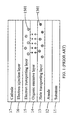
- FIG. 2 illustrates a doped type OLED apparatus proposed by C. H. Chen et al. in Applied Physics Letters, vol. 85, p. 3301 (2004 ).
- the OLED apparatus structure sequentially comprises, from bottom to top, a transparent substrate 18, a transparent anode 19, a hole injection layer 20, a hole transporting layer 21, a dye-doped emissive layer 22, an electron transporting layer 23, an electron injection layer 24, and a metal cathode 25 to emit light.
- FIG. 3 is also a cross-sectional view showing a structure of an OLED apparatus of the prior art, which was proposed by Raychaudhuri et al. of Eastman Kodak Company in TW Pat. No. 497283 (2002) .
- the OLED apparatus structure sequentially comprises, from bottom to top, a transparent substrate 26, a transparent anode 27, a hole injection layer 28, a hole transporting layer 29, an emissive layer 30, an electron transporting layer 31, a first buffer layer 32, a second buffer layer 33, and a metal cathode 34.
- the first buffer layer is of alkali halide
- the second buffer layer is of phthalocyanine.
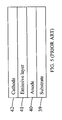
- the OLED apparatus structure sequentially comprises, from bottom to top, a transparent substrate 35, a transparent anode 36, an emissive layer 37, and a metal cathode 38.
- the emissive layer is composed of inorganic quantum dots CuS and ZnS. When a forward bias is applied, holes and electrons can recombine and hence emit light in the emissive layer 37.
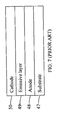
- the OLED apparatus structure sequentially comprises, from bottom to top, a transparent substrate 39, a transparent anode 40, an emissive layer 41, and a metal cathode 42.
- the emissive layer is composed of inorganic composite quantum dots, CdSe/CdS. CdS forms the core of the quantum dot, and CdSe forms the outer shell. When a forward bias is applied, holes and electrons can recombine and hence emit light in the emissive layer 41.
- the OLED apparatus structure sequentially comprises, from bottom to top, a transparent substrate 43, a transparent anode 44, an emissive layer 45, and a metal cathode 46.
- the emissive layer comprises organic/inorganic composite quantum dots incorporated uniformly in an organic material.
- Each organic/inorganic composite quantum dot comprises: (Y 1-x-y Gd x Ce y )Al 5 O 12 , (Y 1-x Ge x ) 3 (Al 1-y Ga y )O 12 , (Y 1-x-y Gd x Ce y ) 3 (Al 5-z Ga z )O 12 or (Gd 1-x Ce x )Sc 2 Al 3 O 12 where 0 ⁇ x ⁇ 1, 0 ⁇ y ⁇ 1, 0 ⁇ z ⁇ 5 and x+y ⁇ 1.
- a forward bias is applied, holes and electrons can recombine and hence emit light in the emissive layer 45.
- the OLED apparatus structure sequentially comprises, from bottom to top, a transparent substrate 47, a transparent anode 48, an emissive layer 49, and a metal cathode 50.
- the emissive layer comprises inorganic composite quantum dots incorporated uniformly in a polymer. Each inorganic composite quantum dot is composed of a II-VI group semiconductor material covering a III-V counterpart.
- the OLED apparatus structure sequentially comprises, from bottom to top, a transparent substrate 51, a transparent anode 52, a hole transporting layer 53, an emissive layer 54, an electron transporting layer 55, and a metal cathode 56.
- the emissive layer is composed of inorganic quantum dots CdSe to emit light. When a forward bias is applied, holes and electrons can recombine and hence emit light in the emissive layer 54.
- FIG. 9 it is shown an OLED apparatus of the prior art.
- the structure was proposed by T. H. Liu et al. in TW Pat. No. 200618664 (2006 ).
- the OLED apparatus structure sequentially comprises, from bottom to top, a transparent substrate 57, a transparent anode 58, a hole transporting layer 59, an emissive layer 60, an electron transporting layer 61, an inorganic layer 62, and a metal cathode 63 to emit light.
- FIG. 10 there is a cross-sectional view showing a structure of another OLED apparatus of the prior art.
- the structure was proposed by J. H. Jou of Tsing Hua University in TW Pat. No. 200608614 (2006 ).
- the OLED apparatus structure sequentially comprises, from bottom to top, a transparent substrate 64, a transparent anode 65, a hole transporting layer 66, and an emissive layer 67 wherein the emissive layer comprises a plurality of organic/inorganic composite quantum dots incorporated in a polymer and each organic/inorganic composite quantum dot comprises: a ZnX quantum dot (X is selected from the group consisting of S, Se, Te and the combination thereof) and an organic molecule covering the surface of the quantum dot, an electron transporting layer 68, and a metal cathode 69.
- X is selected from the group consisting of S, Se, Te and the combination thereof
- an organic molecule covering the surface of the quantum dot an electron transporting layer 68, and a metal cathode 69.
- the OLED apparatus structure sequentially comprises, from bottom to top, a transparent substrate 70, a transparent anode 71, a hole transporting layer 72, an emissive layer 73, an electron transporting layer 74, and a metal cathode 75.
- the hole transporting layer comprises poly(ethylenedioxythiophene): poly(styrene sulfonic acid) (PEDOT: PSS) doped with nano dots.
- the nano dot is synthesized by a sol-gel method and its chemical formula is M x O y where M is metal (titanium (Ti), zinc (Zn), silver (Ag), copper (Cu), nickel (Ni), tin (Sn), iron (Fe)) and inorganic metalloid (silicon (Si)), and O is an oxygen atom.
- M metal (titanium (Ti), zinc (Zn), silver (Ag), copper (Cu), nickel (Ni), tin (Sn), iron (Fe)) and inorganic metalloid (silicon (Si)), and O is an oxygen atom.
- the inventors herein propose an enhanced high efficiency organic light emitting diode with nano-dots synthesized by a sol-gel method and a fabrication method thereof based on their research for many years and plenty of practical experience, thereby accomplishing the foregoing expectations.
- the present invention discloses an organic light emitting diode with nano-dots and a fabrication method thereof.
- the OLED apparatus comprises a substrate, a first electrically conductive layer, a first emission-auxiliary layer, an emissive layer, a second emission-auxiliary layer and a second electrically conductive layer. Its fabrication method is described below. Nano-dots with functional groups on the surface are incorporated into the emissive layer, the first emission-auxiliary layer or the second emission-auxiliary layer to form a layered electro-luminescent structure. By using the fabrication method, the resultant efficiency of the OLEDs can be markedly enhanced.
- FIG. 12 there is a cross-sectional view showing a structure of an OLED according to a preferred embodiment of the present invention.
- the OLED structure sequentially comprises, from bottom to top, a substrate 76, a first electrically conductive layer 77, a first emission-auxiliary layer 78 doped with nano-dots, a dye-doped light emissive layer 79, a second emission-auxiliary layer 80 and a second electrically conductive layer 81.
- the first electrically conductive layer 77 is deposited on the substrate 76.
- the first emission-auxiliary layer 78 doped with nano-dots is deposited on the first electrically conductive layer 77.
- the emissive layer 79 is deposited on the first emission-auxiliary layer 78 doped with nano-dots.
- the second emission-auxiliary 80 is deposited on the emissive layer 79, and the second electrically conductive layer 81 is deposited on the second emission-auxiliary layer 80.
- the dye-doped emissive layer 79 comprises a host material and more than one guest material which can be a fluorescent or phosphorescent emitter.
- the first emission-auxiliary layer 78 doped with nano-dots is a composite of a hole transporting material, poly(ethylenedioxythiophene): poly(styrene sulfonic acid) (PEDOT: PSS), and nano-dots with functional groups on its surface (polymeric nano-dots).
- the chemical formula of the nano-dots is M x O y R z where M is a metal, transition metal, metalloid or metal alloy, O is an oxygen atom and R is an organic group.
- the metal is selected from the group consisting of aluminum (Al), tin (Sn), magnesium (Mg) and calcium (Ca).
- the transition metal is selected from the group consisting of titanium (Ti), manganese (Mn), zinc (Zn), gold (Au), silver (Ag), copper (Cu), nickel (Ni) and iron (Fe).
- the metalloid is silicon (Si).
- the organic group is selected from the group consisting of amino, alkyl, alkenyl and hydroxyl.
- the surface charges of the nano-dots measured by means of an electrophoresis light scattering method are from +1 to +200 mV or from -1 to -200 mV.
- the doping weight percentage of the nano-dots is from 0.1 to 15 wt%, and their particle diameters are in the range of 1 to 30 nm.
- the second emission-auxiliary layer 80 comprises an electron transporting material and an electron injection material.
- the electron transporting material can be 1,3, 5-tris(N-phenyl-benzimidazol-2-yl)benzene (TPBi), tris(8-hydroxyquinoline) aluminum (Alq 3 ), or the like, and the electron injection material can be lithium fluoride (LiF), cesium fluoride (CsF), or the like.
- the second electrically conductive layer 81 can generally be made of electrically conductive materials like aluminum (Al), silver (Ag), etc.
- the substrate 76 can generally be a glass substrate, a plastic substrate or a metal substrate.
- the first electrically conductive layer 77 can generally be an indium tin oxide (ITO) layer or an indium zinc oxide (IZO) layer.
- the first emission-auxiliary layer can be a carrier injection layer, a carrier transporting layer, a carrier blocking layer or an exciton-confining layer.
- the second emission-auxiliary layer can be a carrier injection layer, a carrier transporting layer, a carrier blocking layer or an exciton-confining layer.
- FIG. 13 there is a flow chart of a fabrication method of an OLED according to a preferred embodiment of the present invention.
- the method comprises the following steps:
- the composition of the emissive layer comprises a host material and more than one guest material, comprising a fluorescent emissive material or phosphorescent emissive material.
- the first emission-auxiliary layer doped with the nano-dots is a composite of a hole transporting material, poly(ethylenedioxythiophene): poly(styrene sulfonic acid) (PEDOT: PSS), and nano-dots with functional groups on its surface (polymeric nano-dots).
- the chemical formula of the nano-dots is M x O y R z where M is a metal, transition metal, metalloid or metal alloy, O is an oxygen atom and R is an organic group.
- the metal is selected from the group consisting of aluminum (Al), tin (Sn), magnesium (Mg) and calcium (Ca).
- the transition metal is selected from the group consisting of titanium (Ti), manganese (Mn), zinc (Zn), gold (Au), silver (Ag), copper (Cu), nickel (Ni) and iron (Fe).
- the metalloid is silicon (Si).
- the organic group is selected from the group consisting of amino, alkyl, alkenyl and hydroxyl.
- the surface charges of the nano-dots measured by means of an electrophoresis light scattering method are from +1 to +200 mV or from -1 to -200 mV.
- the doping concentration of the nano-dots is from 0.1 to 15 wt%, and their particle diameters are in the range of 1 to 30 nm.
- the second emission-auxiliary layer comprises an electron transporting material and an electron injection material.
- the electron transporting material can be TPBi and Alq 3 , etc., and the electron injection material can be LiF, CsF, or the like.
- the second electrically conductive layer can generally be made of electrically conductive materials like Al, Ca and Ag, etc.
- the substrate can generally be a glass substrate, a plastic substrate or a metal substrate.
- the first emission-auxiliary layer can be a carrier injection layer, a carrier transporting layer, a carrier blocking layer or an exciton-confining layer.
- the second emission-auxiliary layer can be a carrier injection layer, a carrier transporting layer, a carrier blocking layer or an exciton-confining layer.
- Table 1 it is a comparative table showing the power efficiency of exemplary examples according to the present invention and the comparative example as follows.
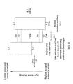
- Example 1 is an OLED apparatus made according to the present invention. With reference to the apparatus structure shown in FIG. 14 and the energy level diagram shown in FIG. 15 , its fabrication method is described below.
- the device was fabricated by a solution process using an ITO coated glass substrate.
- the substrate 88 is cleaned in ultrasonic baths of detergent, de-ionized water, acetone and isopropyl alcohol in turn, and then treated with the boiling hydrogen peroxide.
- the resulted substrate is purged with nitrogen and then placed into a nitrogen glove box for the solution process.
- the first step is to spin coat a 35 nm first emission-auxiliary layer 90 on the pre-cleaned first electrically conductive layer 89 under nitrogen.
- the first emission-auxiliary layer 90 is composed of PEDOT: PSS doped with nano-dots which possesses positive surface-charge.
- the second step is to deposit a 35 nm blue emissive layer 91 via wet-process. A 32 nm electron transporting layer of TPBi is then deposited at 2 ⁇ 10 -5 torr. Finally, a 0.7 nm second emission-auxiliary layer 92 of lithium fluoride and a 150 nm aluminum layer 93 are sequentially deposited on the ITO transparent conductive glass by thermal evaporation.
- aqueous PEDOT: PSS 10 nm of nano-dots possessing positive surface-charge is used to incorporate into aqueous PEDOT: PSS in the first emission-auxiliary layer.
- toluene is used to be the solvent
- the host material of 4,4'-bis(carbazol-9-yl) biphenyl (CBP) doped with 16 wt% blue emitter of bis(3,5-difluoro-2-(2-pyridyl)-phenyl-(2-carboxypyridyl) iridium (III) (FIrpic) is used to prepare the emissive solution.
- the first emission-auxiliary layer doped with the nano-dots possessing positive surface-charge can effectively block holes and increase the electron/hole-injection balance and recombination efficiency, thereby markedly enhancing the efficiency of the OLED.
- the resultant power efficiency at 100 cd/m 2 was increased from 18 to 37 lm/W, an increase of 205.
- the blue OLED exhibits CIE color coordinates of (0.18, 0.35).
- Example 2 is an OLED apparatus made according to the present invention. With reference to the apparatus structure shown in FIG. 16 and the schematic energy level diagram shown in FIG. 17 , 10 nm of nano-dots possessing negative surface-charge is incorporated into aqueous PEDOT: PSS in an appropriate concentration to form an emission-auxiliary material 96.
- the first emission-auxiliary layer suitably doped with the nano-dots possessing positive surface-charge can effectively trap holes and increase the electron/hole-injection balance and recombination efficiency, thereby markedly enhancing the efficiency of the OLED.
- the resultant power efficiency at 100 cd/m 2 was increased from 18 to 31 lm/W, an increase of 172.
- the blue OLED exhibits CIE color coordinates of (0.18, 0.34).
- Comparative Example is an OLED apparatus made according to the prior art.
- the apparatus structure is as shown in FIG. 18 .
- the material of the first emission-auxiliary layer 102 of the OLED structure is PEDOT: PSS.
- the schematic energy level diagram is given for reference in FIG. 19 .
- the OLED made in Comparative Example has unimproved electron/hole-injection balance and recombination efficiency such that the efficiency is significantly reduced, as shown as respective power efficiencies in Table 1.
Landscapes
- Chemical & Material Sciences (AREA)
- Engineering & Computer Science (AREA)
- Materials Engineering (AREA)
- Organic Chemistry (AREA)
- Electroluminescent Light Sources (AREA)
Applications Claiming Priority (1)
| Application Number | Priority Date | Filing Date | Title |
|---|---|---|---|
| CN200897140747 | 2008-10-23 |
Publications (2)
| Publication Number | Publication Date |
|---|---|
| EP2180030A2 true EP2180030A2 (fr) | 2010-04-28 |
| EP2180030A3 EP2180030A3 (fr) | 2010-10-06 |
Family
ID=41785587
Family Applications (1)
| Application Number | Title | Priority Date | Filing Date |
|---|---|---|---|
| EP09012884A Withdrawn EP2180030A3 (fr) | 2008-10-23 | 2009-10-12 | Diode électroluminescente organique avec des points quantiques et son procédé de fabrication |
Country Status (1)
| Country | Link |
|---|---|
| EP (1) | EP2180030A3 (fr) |
Citations (9)
| Publication number | Priority date | Publication date | Assignee | Title |
|---|---|---|---|---|
| US5061569A (en) | 1990-07-26 | 1991-10-29 | Eastman Kodak Company | Electroluminescent device with organic electroluminescent medium |
| TW497283B (en) | 2000-08-11 | 2002-08-01 | Eastman Kodak Co | Improved cathode layer in organic light-emitting diode devices |
| US6602731B2 (en) | 2001-02-07 | 2003-08-05 | Agfa Gevaert | Manufacturing of a thin inorganic light emitting diode |
| US6777724B2 (en) | 2000-11-16 | 2004-08-17 | General Electric Company | Light-emitting device with organic layer doped with photoluminescent material |
| TW200608614A (en) | 2004-08-16 | 2006-03-01 | Ind Tech Res Inst | Organic-inorganic light emitting diode fabrication method |
| TW200618664A (en) | 2004-11-23 | 2006-06-01 | Au Optronics Corp | Organic photoelectric device with improved electron transport efficiency |
| US20060170331A1 (en) | 2003-03-11 | 2006-08-03 | Dietrich Bertram | Electroluminescent device with quantum dots |
| US7132787B2 (en) | 2002-11-20 | 2006-11-07 | The Regents Of The University Of California | Multilayer polymer-quantum dot light emitting diodes and methods of making and using thereof |
| US20070077594A1 (en) | 2003-12-02 | 2007-04-05 | Koninklijke Philips Electronics | Electroluminescent device |
Family Cites Families (1)
| Publication number | Priority date | Publication date | Assignee | Title |
|---|---|---|---|---|
| TWI410162B (zh) * | 2007-06-07 | 2013-09-21 | Nat Univ Tsing Hua | 含奈米點之有機發光二極體裝置結構 |
-
2009
- 2009-10-12 EP EP09012884A patent/EP2180030A3/fr not_active Withdrawn
Patent Citations (9)
| Publication number | Priority date | Publication date | Assignee | Title |
|---|---|---|---|---|
| US5061569A (en) | 1990-07-26 | 1991-10-29 | Eastman Kodak Company | Electroluminescent device with organic electroluminescent medium |
| TW497283B (en) | 2000-08-11 | 2002-08-01 | Eastman Kodak Co | Improved cathode layer in organic light-emitting diode devices |
| US6777724B2 (en) | 2000-11-16 | 2004-08-17 | General Electric Company | Light-emitting device with organic layer doped with photoluminescent material |
| US6602731B2 (en) | 2001-02-07 | 2003-08-05 | Agfa Gevaert | Manufacturing of a thin inorganic light emitting diode |
| US7132787B2 (en) | 2002-11-20 | 2006-11-07 | The Regents Of The University Of California | Multilayer polymer-quantum dot light emitting diodes and methods of making and using thereof |
| US20060170331A1 (en) | 2003-03-11 | 2006-08-03 | Dietrich Bertram | Electroluminescent device with quantum dots |
| US20070077594A1 (en) | 2003-12-02 | 2007-04-05 | Koninklijke Philips Electronics | Electroluminescent device |
| TW200608614A (en) | 2004-08-16 | 2006-03-01 | Ind Tech Res Inst | Organic-inorganic light emitting diode fabrication method |
| TW200618664A (en) | 2004-11-23 | 2006-06-01 | Au Optronics Corp | Organic photoelectric device with improved electron transport efficiency |
Non-Patent Citations (2)
| Title |
|---|
| C. H. CHEN ET AL., APPLIED PHYSICS LETTERS, vol. 85, 2004, pages 3301 |
| C. W. TANG; S. A. VANSLYK ET AL., EASTMAN KODAK COMPANY, 1987 |
Also Published As
| Publication number | Publication date |
|---|---|
| EP2180030A3 (fr) | 2010-10-06 |
Similar Documents
| Publication | Publication Date | Title |
|---|---|---|
| US20100102294A1 (en) | Organic light emitting diode with nano-dots and fabrication method thereof | |
| Han et al. | Elucidating the crucial role of hole injection layer in degradation of organic light-emitting diodes | |
| CN100477873C (zh) | 发光元件及发光装置 | |
| US8222806B2 (en) | Organic light-emitting diode device and manufacturing method thereof | |
| CN102931355B (zh) | Oled器件 | |
| US7919771B2 (en) | Composition for electron transport layer, electron transport layer manufactured thereof, and organic electroluminescent device including the electron transport layer | |
| CN106848084A (zh) | 一种oled显示面板、制作方法及含有其的电子设备 | |
| US20220052262A1 (en) | Method of manufacturing perovskite light emitting device by inkjet printing | |
| EP2787553A1 (fr) | Dispositif électroluminescent organique et procédé de préparation de ce dispositif | |
| CN104037328A (zh) | 有机电致发光器件及其制备方法 | |
| US20220052303A1 (en) | Method of manufacturing perovskite light emitting device by inkjet printing | |
| Parthasarathy et al. | Organic light emitting devices: From displays to lighting | |
| EP2787552A1 (fr) | Dispositif électroluminescent polymère et procédé permettant de préparer ce dispositif | |
| EP2180030A2 (fr) | Diode électroluminescente organique avec des points quantiques et son procédé de fabrication | |
| US20100051997A1 (en) | Organic light emitting diode and method of fabricating the same | |
| TWI410162B (zh) | 含奈米點之有機發光二極體裝置結構 | |
| CN111697145A (zh) | 非掺杂溶液加工型树枝状热活化延迟荧光电致发光二极管 | |
| KR100567220B1 (ko) | 개선된 효율을 갖는 유기 전계발광 소자 및 이에 기초한 디스플레이 장치 | |
| KR100579172B1 (ko) | 유기 전자 발광 소자 | |
| TWI234412B (en) | Organic electroluminescent element | |
| CN1505447A (zh) | 有机电激发光元件 | |
| 김이슬 | Effects of Charge Balance on Device Performances of Solution Processed QLEDs | |
| TWI393479B (zh) | 高效率有機發光二極體及其製造方法 | |
| KR101626149B1 (ko) | 유기발광소자 제조 방법 및 장치 | |
| KR101193181B1 (ko) | 발광층 형성용 조성물 및 고효율 유기전계발광소자 |
Legal Events
| Date | Code | Title | Description |
|---|---|---|---|
| PUAI | Public reference made under article 153(3) epc to a published international application that has entered the european phase |
Free format text: ORIGINAL CODE: 0009012 |
|
| AK | Designated contracting states |
Kind code of ref document: A2 Designated state(s): AT BE BG CH CY CZ DE DK EE ES FI FR GB GR HR HU IE IS IT LI LT LU LV MC MK MT NL NO PL PT RO SE SI SK SM TR |
|
| AX | Request for extension of the european patent |
Extension state: AL BA RS |
|
| PUAL | Search report despatched |
Free format text: ORIGINAL CODE: 0009013 |
|
| AK | Designated contracting states |
Kind code of ref document: A3 Designated state(s): AT BE BG CH CY CZ DE DK EE ES FI FR GB GR HR HU IE IS IT LI LT LU LV MC MK MT NL NO PL PT RO SE SI SK SM TR |
|
| AX | Request for extension of the european patent |
Extension state: AL BA RS |
|
| 17P | Request for examination filed |
Effective date: 20110318 |
|
| 17Q | First examination report despatched |
Effective date: 20120823 |
|
| STAA | Information on the status of an ep patent application or granted ep patent |
Free format text: STATUS: EXAMINATION IS IN PROGRESS |
|
| STAA | Information on the status of an ep patent application or granted ep patent |
Free format text: STATUS: THE APPLICATION IS DEEMED TO BE WITHDRAWN |
|
| 18D | Application deemed to be withdrawn |
Effective date: 20170503 |