EP2180532A2 - Dispositif électroluminescent à semi-conducteur - Google Patents
Dispositif électroluminescent à semi-conducteur Download PDFInfo
- Publication number
- EP2180532A2 EP2180532A2 EP09013440A EP09013440A EP2180532A2 EP 2180532 A2 EP2180532 A2 EP 2180532A2 EP 09013440 A EP09013440 A EP 09013440A EP 09013440 A EP09013440 A EP 09013440A EP 2180532 A2 EP2180532 A2 EP 2180532A2
- Authority
- EP
- European Patent Office
- Prior art keywords
- layer
- light emitting
- electrode
- conductive semiconductor
- emitting device
- Prior art date
- Legal status (The legal status is an assumption and is not a legal conclusion. Google has not performed a legal analysis and makes no representation as to the accuracy of the status listed.)
- Granted
Links
Images




Classifications
-
- H—ELECTRICITY
- H10—SEMICONDUCTOR DEVICES; ELECTRIC SOLID-STATE DEVICES NOT OTHERWISE PROVIDED FOR
- H10H—INORGANIC LIGHT-EMITTING SEMICONDUCTOR DEVICES HAVING POTENTIAL BARRIERS
- H10H20/00—Individual inorganic light-emitting semiconductor devices having potential barriers, e.g. light-emitting diodes [LED]
- H10H20/80—Constructional details
- H10H20/83—Electrodes
- H10H20/831—Electrodes characterised by their shape
- H10H20/8314—Electrodes characterised by their shape extending at least partially onto an outer side surface of the bodies
-
- H—ELECTRICITY
- H10—SEMICONDUCTOR DEVICES; ELECTRIC SOLID-STATE DEVICES NOT OTHERWISE PROVIDED FOR
- H10W—GENERIC PACKAGES, INTERCONNECTIONS, CONNECTORS OR OTHER CONSTRUCTIONAL DETAILS OF DEVICES COVERED BY CLASS H10
- H10W90/00—Package configurations
-
- H—ELECTRICITY
- H10—SEMICONDUCTOR DEVICES; ELECTRIC SOLID-STATE DEVICES NOT OTHERWISE PROVIDED FOR
- H10H—INORGANIC LIGHT-EMITTING SEMICONDUCTOR DEVICES HAVING POTENTIAL BARRIERS
- H10H20/00—Individual inorganic light-emitting semiconductor devices having potential barriers, e.g. light-emitting diodes [LED]
- H10H20/01—Manufacture or treatment
- H10H20/011—Manufacture or treatment of bodies, e.g. forming semiconductor layers
- H10H20/018—Bonding of wafers
-
- H—ELECTRICITY
- H10—SEMICONDUCTOR DEVICES; ELECTRIC SOLID-STATE DEVICES NOT OTHERWISE PROVIDED FOR
- H10H—INORGANIC LIGHT-EMITTING SEMICONDUCTOR DEVICES HAVING POTENTIAL BARRIERS
- H10H20/00—Individual inorganic light-emitting semiconductor devices having potential barriers, e.g. light-emitting diodes [LED]
- H10H20/80—Constructional details
- H10H20/84—Coatings, e.g. passivation layers or antireflective coatings
-
- H—ELECTRICITY
- H10—SEMICONDUCTOR DEVICES; ELECTRIC SOLID-STATE DEVICES NOT OTHERWISE PROVIDED FOR
- H10H—INORGANIC LIGHT-EMITTING SEMICONDUCTOR DEVICES HAVING POTENTIAL BARRIERS
- H10H29/00—Integrated devices, or assemblies of multiple devices, comprising at least one light-emitting semiconductor element covered by group H10H20/00
- H10H29/10—Integrated devices comprising at least one light-emitting semiconductor component covered by group H10H20/00
Definitions
- the present disclosure relates to a semiconductor light emitting device.
- III-V nitride semiconductors have been in the spotlight as a core material for light emitting devices, such as light emitting diodes (LEDs), laser diodes (LDs), and the like, due to excellent physical and chemical properties thereof.
- the III-V nitride semiconductor includes a semiconductor material having the formula In x AlyGa 1-x-y N (where 0 ⁇ x ⁇ 1, 0 ⁇ y ⁇ 1, 0 ⁇ x+y ⁇ 1).
- a Light Emitting Diode is a kind of semiconductor device that converts electricity into infrared rays or light using the characteristics of a compound semiconductor to transmit and receive a signal, or is used as a light source.
- the LEDs or Laser diodes (LDs) made of these nitride semiconductor materials are extensively adopted in light emitting devices for obtaining light, and are applied as a light source for various products such as a keypad light emitting diode of a mobile phone, an electrical sign board, and a lighting device.
- LDs Laser diodes
- Embodiments provide a semiconductor light emitting device with a capacitor structure.
- Embodiments provide a semiconductor light emitting device to improve ESD (electro-static discharge) characteristics by disposing an insulating layer between a metal layer and a second electrode layer to embody a capacitor.
- ESD electro-static discharge
- An embodiment provides a semiconductor light emitting device comprising: a light emitting structure comprising a plurality of compound semiconductor layers; a first electrode under the light emitting structure; a second electrode layer on the light emitting structure; a first insulating layer between the light emitting structure and the second electrode layer; and a metal layer formed under the first insulating layer and electrically connected to the first electrode.
- An embodiment provides a semiconductor light emitting device comprising: a light emitting structure comprising a first conductive semiconductor layer, an active layer on the first conductive semiconductor layer, and a second conductive semiconductor layer on the active layer; a first electrode under the first conductive semiconductor layer; a second electrode layer on the second conductive semiconductor layer; a second insulating layer on an outer side of the light emitting structure; a first insulating layer under the second electrode layer; and a metal layer comprising a loop pattern under a circumference of the first insulating layer and a connection pattern electrically connected to the first electrode on the second insulating layer.
- An embodiment provides a semiconductor light emitting device comprising: a first conductive semiconductor layer; an active layer on the first conductive semiconductor layer; a second conductive semiconductor layer on the active layer; a first electrode under the first conductive semiconductor layer; a second electrode layer on the second conductive semiconductor layer; a first insulating layer between the second conductive semiconductor layer and the second electrode layer; and a metal layer formed under the first insulating layer and electrically connected to the first electrode, wherein the first insulating layer comprises a protrusion disposed in a closed loop shape on a certain regions from the second conductive semiconductor layer to the upper portion of the first conductive semiconductor layer.
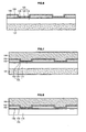
- Fig. 1 is a side-sectional view of a semiconductor light emitting device according to a first embodiment.
- Fig. 2A is a plan view of Fig. 1 .
- Fig. 3 is a circuit diagram illustrating an equivalent circuit of Fig. 1 .
- Figs. 4 to 11 are diagrams illustrating a process of manufacturing the semiconductor light emitting device in Fig. 1 .
- Fig. 12 is a side-sectional view of a semiconductor light emitting device according to a second embodiment.
- Fig. 13 is a bottom view of Fig. 11 .
- Fig. 14 is a side-sectional view of a semiconductor light emitting device according to a third embodiment.
- Fig. 15 a bottom view of a semiconductor light emitting device according to a fourth embodiment.
- Fig. 1 is a side-sectional view of a semiconductor light emitting device according to a first embodiment
- Fig. 2 is a plan view of Fig. 1
- Fig. 3 is a circuit diagram illustrating an equivalent circuit of Fig. 1 .
- a semiconductor light emitting device 100 includes a light emitting structure 135, a first insulating layer 140, a second electrode layer 150, a conductive supporting member 160, a second insulating layer 180, and a metal layer 190.
- the light emitting structure 135 includes an LED using a plurality of compound semiconductor layers, for example, group III-V compound semiconductors, and the LED may be a colored LED or a UV LED which emits blue light, green light, or red light. Light emitted by the LED may be diversely implemented within the technical scope of embodiments.
- the compound semiconductor may have, but is not limited to, a formula of In x AlyGa 1-x-y N (where 0 ⁇ x ⁇ 1, 0 ⁇ y ⁇ 1, 0 ⁇ x+y ⁇ 1).
- the light emitting structure 135 includes a first conductive semiconductor layer 110, an active layer 120, and a second conductive semiconductor layer 130.
- the first conductive semiconductor layer 110 may be formed of at least one of the compound semiconductors of group III-V elements doped with a first conductive dopant, for example, GaN, AlN, AlGaN, InGaN, InN, InAlGaN, AlInN, AlGaAs, GaP, GaAs, GaAsP, and AlGaInP.
- a first conductive dopant for example, GaN, AlN, AlGaN, InGaN, InN, InAlGaN, AlInN, AlGaAs, GaP, GaAs, GaAsP, and AlGaInP.
- the first conductive dopant includes an N-type dopant such as si, Ge, Sn, Se, and Te.
- the first conductive semiconductor layer 110 may be formed in a mono- or multi-layer, but is not limited thereto.
- a first electrode 171 is formed under the first conductive semiconductor layer 110, and the first electrode 171 may be formed in a predetermined pattern with a predetermined shape, but is not limited thereto.
- the first electrode 171 may include a bonding pad.
- the first electrode 171 may be formed using a material selected from the group consisting of, but is not limited to, Ti, Al, In, Ta, Pd, Co, Ni, Si, Ge, Ag, and Au.
- the active layer 120 is formed on the first conductive semiconductor layer 110, and may be formed in a single quantum well structure or a multiple quantum well structure.
- the active layer 120 may be periodically formed by the structure of a well layer and a barrier layer, for example, an InGaN well layer/GaN barrier layer by using the compound semiconductor material of group III-V elements.
- a conductive clad layer may be formed on and/or under the active layer 120, and the conductive clad layer may be formed of an AlGaN-based semiconductor.
- the second conductive semiconductor layer 130 is formed on the active layer 120, and may be formed of at least one of the compound semiconductors of group III-V elements doped with a second conductive dopant, for example, GaN, AlN, AlGaN, InGaN, InN, InAlGaN, AlInN, AlGaAs, GaP, GaAs, GaAsP, and AlGaInP.
- a second conductive dopant for example, GaN, AlN, AlGaN, InGaN, InN, InAlGaN, AlInN, AlGaAs, GaP, GaAs, GaAsP, and AlGaInP.
- the second conductive dopant includes a P-type dopant such as Mg and Zn.
- the second conductive semiconductor layer 130 may be formed in a mono- or multi-layer, but is not limited thereto.
- the first conductive semiconductor layer 110, the active layer 120, and the second conductive semiconductor layer 130 may be defined as a light emitting structure 135.
- an N-type semiconductor layer or a P-type semiconductor layer may be also provided on the second conductive layer 120.
- the first conductive semiconductor layer 110 may include a P-type semiconductor layer
- the second conductive semiconductor layer 130 may include an N-type semiconductor layer.
- the light emitting structure 135 may include at least one selected from the group consisting of an N-P junction, a P-N junction, an N-P-N junction, and a P-N-P junction.
- the first insulating layer 140 is formed on the top circumference of the second conductive semiconductor layer 130.
- the first insulating layer 140 may be formed in a continuous pattern with a belt shape, a loop shape, and a frame shape on the circumference region of the second conductive semiconductor layer 130.
- the first insulating layer 140 may be formed of a transparent insulating material, which may include SiO 2 , SiO x , SiO x N y , or Si 3 N 4 .
- the first insulating layer 140 may improve adhesive force with a material for the second conductive semiconductor layer 130.
- the first insulating layer 140 may be formed with a width or thickness of 2 ⁇ m or less, but is not limited thereto.
- the outer side of the first insulating layer 140 is exposed to the outer circumference 105 of the first conductive semiconductor layer 110, the active layer 120, and the second conductive semiconductor layer 130. Accordingly, the first insulating layer 140 may separate the second electrode layer 150 from the second conductive semiconductor layer 130.
- a laser irradiated during the manufacturing process is transmitted through the first insulating layer 140 to solve the side delamination of the light emitting structure 135.
- the first insulating layer 140 may also prevent metal debris generated by the second electrode layer 150 or the conductive supporting member 160 from being introduced into the outer side of the semiconductor layer 110, 120, and 130.
- the first insulating layer 140 may inhibit moisture from being penetrated into the outer side of the semiconductor layer 110, 120, and 130.
- a second electrode layer may be formed on the first insulating layer 140 and the second conductive semiconductor layer 130.
- the second electrode layer may include the second electrode layer 150 and the conductive supporting member 160.
- the second electrode layer 150 is formed at the outer side of the top of the second conductive semiconductor layer 130, which may be comprised at least one of an ohmic contact layer, a reflective layer, a adhesive layer and a seed metal.
- the ohmic contact layer may be formed in the form of a layer or a plurality of patterns.
- the ohmic contact layer may be comprised at least one of a metal material and an oxide material.
- the ohmic contact layer may comprise at least one selected from the group consisting of ITO, IZO, IZTO, IAZO, IGZO, IGTO, AZO, ATO, GZO, IrOx, RuOx, RuOx/ITO, Ni/IrOx/Au, Ni/IrOx/Au/ITO, Pt, Ni, Au, Rh and Pd .
- the ohmic contact layer may have a thickness of about 10 ⁇ to about 1 ⁇ m . However, the embodiment is not limited thereto.
- the reflective layer may be formed at least one of layers and formed of at least one of Ag, Ni, Al, Rh, Pd, Ir, Ru, Mg, Zn, Pt, Au and Hf, and materials consisting of the selective combination of these elements.
- the adhesive layer may be formed at least one of layers and formed of at least one of Ti, Au, Sn, Ni, Cr, Ga, In, Bi, Cu, Ag, and Ta, and materials consisting of the selective combination of these elements.
- the second electrode layer 150 may be used as a seed layer for a plating process.
- the seed layer may be formed at least one of Ti, Cr, Ta, Cr/Au, Cr/Cu, Ti/Au, Ta/Cu, and Ta/Ti/Cu.
- the conductive supporting member 160 may be formed on the second electrode layer 150.
- the conductive supporting member 160 may function as a base substrate, and its material may include copper (Cu), gold (Au), nickel (Ni), molybdenum (Mo), copper-tungsten (Cu-W), and carrier wafer such as Si, Ge, GaAs, ZnO, and SiC, SiGe, and GaN.
- the conductive supporting member 160 may be formed by an electroplating technique or in the form of a sheet, but is not limited thereto.
- the conductive supporting member 160 may be formed with a thickness of about 30 ⁇ m to about 150 ⁇ m, but is not limited thereto.
- a second insulating layer 180 is formed at the outer side of the light emitting structure 135.
- the second insulating layer 180 is formed along the outer side of the first conductive semiconductor layer 110, the active layer 120, and the second conductive semiconductor layer 130, and one end 181 is disposed under some portions of the first electrode 171 and the other end is disposed under the first insulating layer 140.
- the metal layer 190 includes a connection pattern 191 and a loop pattern 193.
- the connection pattern 191 is formed under the second insulating layer 180, one end is electrically connected to the first electrode 171, and the other end is electrically connected to the loop pattern 193.
- the second insulating layer 180 is disposed between the connection pattern 191 of the metal layer 190 and the semiconductor layer 110, 120, and 130 to insulate them.
- the metal layer 190 may be formed in a mono- or multi-layer of at least one selected from the group consisting of Ti, Al, In, Ta, Pd, co, Ni, Si, Ge, Ag, Au, and an alloy thereof.
- the loop pattern 193 is electrically connected to the connection pattern 191 of the metal layer 190, and disposed along the bottom circumference of the first insulating layer 140. Accordingly, the loop pattern 193 of the metal layer 190 and the second electrode layer face each other on both sides of the first insulating layer 140.
- a first current path passing through the light emitting structure 135 and a second current path corresponding to the first insulating layer 140 may be disposed in parallel.
- the first insulating layer 140 functions as a capacitor 100B between the loop pattern 193 of the metal layer 190 and the second electrode layer 150, and the capacitor 100B is parallel connected to both ends P1 and P2 of the light emitting device 100A.
- the capacitor 100B may charge and discharge an ESD voltage applied to the light emitting structure 100 to protect the semiconductor layer 110, 120, and 130 of the light emitting structure 135. Accordingly, a device having characteristic which is robust against ESD may be provided by including a built-in capacitor 100B.
- the capacitance of the capacitor 100B may be controlled to line width or thickness of the metal layer 190, and then may be controlled in consideration of electrical characteristics of the light emitting structure 135.
- Figs. 4 to 11 are diagrams illustrating a process of manufacturing the semiconductor light emitting device in Fig. 1
- a substrate 100 is loaded into growth equipment, and a compound semiconductor layer of group II to group VI elements is formed thereon.
- the growth equipment may include an electron beam evaporator, physical vapor deposition (PVD), chemical vapor deposition (CVD), plasma laser deposition (PLD), dual-type thermal evaporator, sputtering and metal organic chemical vapor deposition (MOCVD), but is not limited thereto.
- PVD physical vapor deposition
- CVD chemical vapor deposition
- PLD plasma laser deposition
- MOCVD metal organic chemical vapor deposition
- the substrate 101 may be selected from the group consisting of sapphire substrate (Al 2 O 3 ), GaN, SiC, ZnO, Si, GaP, InP, Ga 2 O 3 , conductive substrate, and GaAs.
- a concave-convex pattern may be formed on the top of the substrate 101.
- a layer or pattern using a compound semiconductor of group II to group VI elements, for example, at least one selected from the group consisting of ZnO layer (not shown), buffer layer (not shown), and undoped semiconductor layer (not shown) may be formed.
- the buffer layer and the undoped semiconductor layer may be formed using a compound semiconductor of group III-V elements, the buffer layer may decrease a lattice constant difference with the substrate, and the undoped semiconductor layer may be formed of an undoped GaN-based semiconductor.
- a light emitting structure 135 including a plurality of compound semiconductor layers may be formed on the substrate 101.
- the light emitting structure 135 includes a first conductive semiconductor layer 110, an active layer 120, and a second conductive semiconductor layer 130.
- the first conductive semiconductor layer 110 is formed on the substrate 101 or another semiconductor layer
- the active layer 120 is formed on the first conductive semiconductor layer 110
- the second conductive semiconductor layer 130 is formed on the active layer 120.
- the first conductive semiconductor layer 110 may be formed of at least one of the compound semiconductors of group III-V elements doped with a first conductive dopant, for example, GaN, AlN, AlGaN, InGaN, InN, InAlGaN, AlInN, AlGaAs, GaP, GaAs, GaAsP, and AlGaInP.
- a first conductive dopant for example, GaN, AlN, AlGaN, InGaN, InN, InAlGaN, AlInN, AlGaAs, GaP, GaAs, GaAsP, and AlGaInP.
- the first conductive dopant includes an N-type dopant such as si, Ge, Sn, Se, and Te.
- the first conductive semiconductor layer 110 may be formed in a mono- or multi-layer, but is not limited thereto.
- An active layer 120 is formed on the first conductive semiconductor layer 110, and the active layer 120 may be formed in a single quantum well structure or a multiple quantum well structure.
- the active layer 120 may be periodically formed by a well layer and a barrier layer, for example, an InGaN well layer/GaN barrier layer by using the compound semiconductor material of group III-V elements.
- a conductive clad layer may be formed on and/or under the active layer 120, and the conductive clad layer may be formed of an AlGaN-based semiconductor.
- the second conductive semiconductor layer 130 is formed on the active layer 120, and the second conductive semiconductor layer 130 may be formed of at least one of the compound semiconductors of group III-V elements doped with a second conductive dopant, for example, GaN, AlN, AlGaN, InGaN, InN, InAlGaN, AlInN, AlGaAs, GaP, GaAs, GaAsP, and AlGaInP.
- the second conductive dopant includes a P-type dopant such as Mg and Zn.
- the second conductive semiconductor layer 130 may be formed in a mono- or multi-layer, but is not limited thereto.
- a third conductive semiconductor layer for example, an N-type semiconductor layer or a P-type semiconductor layer may be formed on the second conductive semiconductor layer 130. Accordingly, at least one selected from the group consisting of an N-P junction, a P-N junction, an N-P-N junction, and a P-N-P junction structure may be formed in the light emitting structure 135.
- a mask pattern is used on a chip boundary region on the second conductive semiconductor layer 130 to form a first insulating layer 140.
- the first insulating layer 140 is formed along the outer circumference of the top of the second conductive semiconductor layer 130 of an individual chip, and the shape may be formed in a continuous pattern with a belt shape, a loop shape, and a frame shape (eg: closed loop shape). In this case, the inner region of the second conductive semiconductor layer 130 is exposed.
- the first insulating layer 140 may be formed of at least one selected from transparent insulating materials with a predetermined dielectric constant, for example, the group consisting of SiO 2 , SiO x , SiO x N y , and Si 3 N 4 , but is not limited thereto.
- the first insulating layer 140 is formed of a material which is transmitted by laser light and has little debris generated by laser light and may improve adhesive force with the second conductive semiconductor layer 130.
- the first insulating layer 140 may be formed with a width or thickness of 2 ⁇ m or less, but is not limited thereto.
- a second electrode layer 150 is formed on the second conductive semiconductor layer 130 and the first insulating layer 140.
- the second electrode layer 150 may comprise at least one of an ohmic contact layer, a reflective layer, and an adhesive layer.
- the ohmic contact layer may be formed in the form of a layer or a plurality of patterns.
- the ohmic contact layer may be comprised at least one of a metal material and an oxide material.
- the ohmic contact layer may comprise at least one selected from the group consisting of ITO, IZO, IZTO, IAZO, IGZO, IGTO, AZO, ATO, GZO, IrOx, RuOx, RuOx/ITO, Ni/IrOx/Au, Ni/IrOx/Au/ITO, Pt, Ni, Au, Rh and Pd .
- the ohmic contact layer may have a thickness of about 10 ⁇ to about 1 ⁇ m. However, the embodiment is not limited thereto.
- the reflective layer may be formed at least one of layers and formed of at least one of Ag, Ni, Al, Rh, Pd, Ir, Ru, Mg, Zn, Pt, Au and Hf, and materials consisting of the selective combination of these elements.
- the adhesive layer may be formed at least one of layers and formed of at least one of Ti, Au, Sn, Ni, Cr, Ga, In, Bi, Cu, Ag, and Ta, and materials consisting of the selective combination of these elements.
- the second electrode layer 150 may be used as a seed layer for a plating process.
- the seed layer may be formed at least one of Ti, Cr, Ta, Cr/Au, Cr/Cu, Ti/Au, Ta/Cu, and Ta/Ti/Cu.
- a conductive supporting member 160 may be formed on the second conductive layer 150, the conductive supporting member 160 may function as a base substrate, and its material may include copper (Cu), gold (Au), nickel (Ni), molybdenum (Mo), copper-tungsten (Cu-W), and carrier wafer such as Si, Ge, GaAs, ZnO, and SiC, SiGe, and GaN.
- the conductive supporting member 160 may be formed by an electroplating technique or in the form of a sheet, but is not limited thereto.
- the conductive supporting member 160 may be formed with a thickness of about 30 ⁇ m to about 150 ⁇ m, but is not limited thereto.
- the conductive supporting member 160 is disposed on the base to remove the substrate 101.
- the substrate 101 is removed through a physical and/or chemical method.
- the physical removal method separates the substrate 101 by irradiating a laser of a predetermined wavelength on the substrate 101 (Laser Lift Off: LLO).
- the substrate 101 may be separated by removing the buffer layer through a chemical removal method using a wet etchant.
- the substrate removal method is not limited to the chemical removal method.
- a polishing process may be performed by an inductively coupled plasma/reactive ion etching (ICP/RIE) method on the surface of the first conductive semiconductor layer 110 with the substrate 101 removed.
- ICP/RIE inductively coupled plasma/reactive ion etching
- isolation etching is performed on the chip-to-chip boundary region (ie, channel region) to separate the region into chip units. Then, the outer circumference 105 of the light emitting structure 135 is etched to expose the first insulating layer 140. In this case, outer side of the first insulating layer 140 is exposed to the outer circumference 105 of the light emitting structure 135, and the outer circumference of the first insulating layer 140 may separate the second electrode layer 150 from the side wall of the light emitting structure 135.
- the light emitting structure 135 has an effect of being inwardly shifted from the outer wall of the chip.
- a first electrode 171 is formed under the first conductive semiconductor layer 110.
- the first electrode 171 may be formed in a predetermined shape and a predetermined pattern, but is not limited thereto.
- a process of forming the first electrode 171 may be performed before or after the isolation etching or after the chip separation, but is not limited thereto.
- a second insulating layer 180 is formed on a predetermined region of the light emitting structure 135 using a mask pattern.
- the second insulating layer 180 is formed with a predetermined width extending from the first electrode 171 to the position of the first insulating layer 140 to cover the bottom of the first conductive semiconductor layer 110 and some portions of the side wall of the semiconductor layer 110, 120, and 130.
- an end 181 of the second insulating layer 180 may be extended into the bottom of the first electrode 171.
- the second insulating layer 180 may be formed of one selected from the group consisting of SiO 2 , SiO x , SiO x N y , and Si 3 N 4 , or formed of a material identical to the first insulating layer 140 or another material.
- a metal layer 190 is formed under the second insulating layer 180 and the first insulating layer 140, and the metal layer 190 includes a connection pattern 191 and a loop pattern 193.
- the connection pattern 191 of the metal layer 190 is formed under (ie, at the outer side of) the second insulating layer 180, and is electrically connected to the first electrode 171.
- the loop pattern 193 of the metal layer 190 is connected to the other end of the connection pattern 191, is disposed along the bottom circumference of the first insulating layer 140, and is separated from the outer wall of the light emitting structure 135.
- the loop pattern 193 may be formed in an open loop shape or a closed loop shape along the bottom circumference of the first insulating layer 140.
- the metal layer 190 may be formed in a mono- or multi-layer of at least one selected from the group consisting of Ti, In, Ta, Pd, Co, Ni, Si, Ge, Ag, Au, and an alloy thereof.
- connection pattern 191 of the metal layer 190 is electrically connected to the first electric 171, and the loop pattern 193 is disposed to correspond to the second electrode 150.
- the loop pattern 193 of the metal layer 190 may be formed in a pattern shape with a predetermined width under the first insulating layer 140, that is, may be formed in a structure as in Fig. 2 . Then, the first insulating layer 140 is disposed between the loop pattern 193 of the metal layer 190 and the second electrode 150 to function as a capacitor.
- the capacitor is formed in a parallel structure with respect to the light emitting structure 135 to be charged or discharged by an abnormal power source (eg: ESD) applied to the light emitting structure 135. Accordingly, the light emitting structure 135 may be protected from the abnormal power source.
- ESD abnormal power source
- the semiconductor light emitting device is separated into chip units based on the boundary of the chips. Then, laser may be used for a chip separation method.
- the chip may provide a vertical semiconductor light emitting device with a capacitor.
- Fig. 12 is a side-sectional view of a semiconductor light emitting device according to a second embodiment
- Fig. 13 is a bottom view of Fig. 11 .
- description of the second embodiment a repeated description about the portion identical to the first embodiment will be omitted with reference to the first embodiment.
- a semiconductor light emitting device 100A includes a light emitting structure 135, a insulating layer 140A with an protrusion 145, a second electrode layer 150, a conductive supporting member 160, and a metal layer 190.
- the insulating layer 140A may be formed in a continuous pattern (eg: closed loop shape) with a belt shape, a loop shape, and a frame shape on the bottom circumference of the second conductive semiconductor layer 130.
- the insulating layer 140A may include at least one selected from translucent insulating layers, for example, the group consisting of SiO 2 , SiO x , SiO x N y , Si 3 N 4 , Al 2 O 3 , and TiO 2 by using a mask pattern.
- a second conductive layer 150 and the conductive supporting member 160 are formed on the insulating layer 140A and the second conductive semiconductor layer 130.
- a protrusion 145 is formed under the inner side of the insulating layer 140.
- the protrusion 145 may be formed with a depth at which the first conductive semiconductor layer 110 is exposed.
- the protrusion 145 of the insulating layer 140 may be formed in a continuously closed loop shape such as a belt shape or a loop shape, may be formed within a distance of about 1 ⁇ m to about 5 ⁇ m (D1) from the outer wall of the semiconductor layer 110, 120, and 130, and the distance range may be varied according to the size of the chip.
- the cross-sectional shape of the protrusion 145 may be formed in a domed shape, a semi-elliptical shape, a horn shape, a truncated-horn shape, and a polygon shape and the shape may be modified.
- the protrusion 145 of the insulating layer 140A may separate the light emitting structure 135 into an inner active region A1 and an outer inactive region A2.
- the semiconductor layer 110, 120, and 130 in the active region A1 is normally operated, and the semiconductor layer in the inactive region A2 is not normally operated.
- a first conductive semiconductor layer 110 in the inactive region A2 may be used partially in current path.
- a second insulating layer 180 in Fig. 1 may not be formed under the connection pattern 191 of the metal layer 190. Accordingly, a process of forming the second insulating layer may be removed.
- connection pattern 191 of the metal layer 190 and the semiconductor layer 110, 120, and 130 of the light emitting structure 135 may be solved by the protrusion 145 of the insulating layer 140A.
- the loop pattern 193 of the metal layer 190 may not be separated from the outer side of the light emitting structure 135.
- the active region is normally operated because the protrusion 145 of the insulating layer 140A inactivates the outer side of the light emitting structure 135.
- the protrusion 145 of the active layer 140A may prevent moisture from being penetrated into the outer side of the chip. Because the protrusion 145 of the insulating layer 140 may be formed in a single or a double concave-convex structure, it may reinforce adhesive force with the light emitting structure 135.
- Fig. 14 is a side-sectional view of a semiconductor light emitting device according to a third embodiment.
- a repeated description about the portion identical to the second embodiment will be omitted with reference to the second embodiment.
- a semiconductor light emitting device 100B includes a light emitting structure 135, a insulating layer 140A with an protrusion 145A, a second electrode layer 150, a conductive supporting member 160, and a metal layer 190.
- the insulating layer 140A may be formed in a continuous pattern (eg: closed loop shape) with a belt shape, a loop shape, and a frame shape on the bottom circumference of the second conductive semiconductor layer 130.
- the insulating layer 140A may include at least one selected from translucent insulating layers, for example, the group consisting of SiO 2 , SiO x , SiO x N y , Si 3 N 4 , Al 2 O 3 , and TiO 2 by using a mask pattern.
- a second conductive layer 150 and the conductive supporting member 160 are formed on the insulating layer 140A and the second conductive semiconductor layer 130.
- a protrusion 145A is formed under the inner side of the insulating layer 140.
- the protrusion 145A may be formed with a depth at which the first conductive semiconductor layer 110 is exposed.
- the protrusion 145A of the insulating layer 140 may be formed in a continuously closed loop shape such as a belt shape or a loop shape, may be formed to the outer wall of the semiconductor layer 110, 120, and 130.
- the cross-sectional shape of the protrusion 145A may be formed in a polygon shape, a semi-elliptical shape, a horn shape, a truncated-horn shape, and a domed shape and the shape may be modified.
- An outer wall of the light emitting structure 135 is electrically opened by the protrusion 145A of the insulating layer 140A. Accordingly, the second insulating layer is not formed on the light emitting structure 135.
- the protrusion 145A of the insulating layer 140A may be formed on the circumference of the region, on which a loop pattern 193 of the metal layer 190 is disposed, to inactivate the region.
- the area of the active layer 120 may be increased with respect to the active layer of the second embodiment.
- Fig. 15 a bottom view of a semiconductor light emitting device according to a fourth embodiment.
- a repeated description about the portion identical to the embodiments will be omitted with reference to the embodiments.
- a semiconductor light emitting device an insulating layer 140 with a protrusion 145B, a second electrode layer 150, a conductive supporting member 160, and a metal layer 190.
- the insulating layer 140 may be formed in a continuous pattern (eg: closed loop shape) with a belt shape, a loop shape, and a frame shape on the bottom circumference of the second conductive semiconductor layer 130.
- a protrusion 145B is formed under the inner side of the insulating layer 140.
- the protrusion 145B of the insulating layer may be formed with a depth at which the first conductive semiconductor layer 110 is exposed and contacted to the first conductive semiconductor 110.
- the protrusion 145A of the insulating layer 140 may be formed in a continuously closed loop shape such as a belt shape or a loop shape, may be formed to a portion area of the semiconductor layer 110, 120, and 130.
- the opened portion area of the light emitting structure 135 is electrically opened by the protrusion 145B of the insulating layer 140. Accordingly, the second insulating layer is not formed on the light emitting structure 135.
- the protrusion 145B of the insulating layer 140 may be formed on the circumference of the opened portion area, on which a connection pattern 191 of the metal layer 190 is disposed, to inactive region A1. In this case, the area of the active layer 120 may be increased.
- the metal layer 190 includes a connection pattern 191 and a loop pattern 193.
- the connection pattern 191 is electrically connected to the first electrode 171, and the other end is electrically connected to the loop pattern 193.
- the connection pattern 191 is disposed to the opened portion area or the inactive region A1.
- the loop pattern 193 is electrically connected to the connection pattern 191 of the metal layer 190, and disposed along the bottom circumference of the first insulating layer 140. Accordingly, the loop pattern 193 of the metal layer 190 and the second electrode layer face each other on both sides of the first insulating layer 140.
- a first current path passing through the light emitting structure 135 and a second current path corresponding to the first insulating layer 140 may be disposed in parallel.
- a method for manufacturing a semiconductor light emitting device comprising: forming a plurality of compound semiconductor layers to form a light emitting structure; forming a first insulating layer on the top circumference of the light emitting structure; forming a second electrode layer on the first insulating layer and the light emitting structure; forming a first electrode under the light emitting structure; and forming a metal layer comprising a loop pattern on the bottom circumference of the first insulating layer and a connection pattern connected to the first electrode.
- first and second embodiments were centered on each embodiment, the description may be performed by applying the first embodiment in combination with the second embodiment, and the second embodiment in combination with the first embodiment, but is not limited to characteristics of each embodiment.
- Embodiments can provide a vertical semiconductor light emitting device including a built-in capacitor.
- Embodiments can provide a vertical semiconductor light emitting device robust against ESD.
- Embodiments can provide a light emitting device robust against moisture by opening the outer side of the light emitting structure.
- Embodiments can improve adhesive force between a semiconductor layer and another layer.
- Embodiments can prevent interlayer short defects of a plurality of compound semiconductor layers.
- Embodiments can improve the reliability of the vertical semiconductor light emitting device.
- Embodiments can provide a semiconductor light emitting device like LED.
- Embodiments can improve the electrical reliability of the semiconductor light emitting device.
- Embodiments can improve the light efficiency of the vertical semiconductor light emitting device.
- Embodiments can apply a light source including a packaged semiconductor light emitting device to an illumination field, an indication field, and a display field.
Landscapes
- Led Devices (AREA)
Applications Claiming Priority (1)
| Application Number | Priority Date | Filing Date | Title |
|---|---|---|---|
| KR1020080105257A KR100999688B1 (ko) | 2008-10-27 | 2008-10-27 | 반도체 발광소자 및 그 제조방법 |
Publications (3)
| Publication Number | Publication Date |
|---|---|
| EP2180532A2 true EP2180532A2 (fr) | 2010-04-28 |
| EP2180532A3 EP2180532A3 (fr) | 2011-07-20 |
| EP2180532B1 EP2180532B1 (fr) | 2017-06-21 |
Family
ID=41557455
Family Applications (1)
| Application Number | Title | Priority Date | Filing Date |
|---|---|---|---|
| EP09013440.4A Not-in-force EP2180532B1 (fr) | 2008-10-27 | 2009-10-23 | Dispositif électroluminescent à semi-conducteur |
Country Status (4)
| Country | Link |
|---|---|
| US (1) | US7999282B2 (fr) |
| EP (1) | EP2180532B1 (fr) |
| KR (1) | KR100999688B1 (fr) |
| CN (1) | CN101728411B (fr) |
Cited By (3)
| Publication number | Priority date | Publication date | Assignee | Title |
|---|---|---|---|---|
| EP2814061A1 (fr) * | 2013-06-10 | 2014-12-17 | LG Innotek Co., Ltd. | Dispositif à diode électroluminescente et boîtier |
| EP2187455B1 (fr) * | 2008-11-14 | 2018-03-07 | LG Innotek Co., Ltd. | Dispositif électroluminescent semi-conducteur |
| CN115708229A (zh) * | 2021-08-18 | 2023-02-21 | 隆达电子股份有限公司 | 发光二极管晶片与发光二极管晶片装置 |
Families Citing this family (17)
| Publication number | Priority date | Publication date | Assignee | Title |
|---|---|---|---|---|
| JP4702442B2 (ja) * | 2008-12-12 | 2011-06-15 | ソニー株式会社 | 半導体発光素子及びその製造方法 |
| KR100999733B1 (ko) * | 2010-02-18 | 2010-12-08 | 엘지이노텍 주식회사 | 발광 소자, 발광 소자 제조방법 및 발광 소자 패키지 |
| US8338317B2 (en) | 2011-04-06 | 2012-12-25 | Infineon Technologies Ag | Method for processing a semiconductor wafer or die, and particle deposition device |
| KR101039939B1 (ko) * | 2010-04-28 | 2011-06-09 | 엘지이노텍 주식회사 | 발광소자, 발광소자의 제조방법, 발광소자 패키지 및 이를 포함하는 조명시스템 |
| KR101689164B1 (ko) * | 2010-07-21 | 2016-12-23 | 엘지이노텍 주식회사 | 발광소자 |
| KR101683583B1 (ko) * | 2010-07-21 | 2016-12-07 | 엘지이노텍 주식회사 | 발광 소자 |
| TWI493756B (zh) * | 2010-11-15 | 2015-07-21 | 晶元光電股份有限公司 | 發光元件 |
| CN102479902B (zh) * | 2010-11-23 | 2017-04-12 | 晶元光电股份有限公司 | 发光组件 |
| TWI418065B (zh) * | 2011-02-22 | 2013-12-01 | Lextar Electronics Corp | 發光二極體 |
| KR101886156B1 (ko) * | 2012-08-21 | 2018-09-11 | 엘지이노텍 주식회사 | 발광소자 |
| KR101436123B1 (ko) * | 2013-07-09 | 2014-11-03 | 피에스아이 주식회사 | 초소형 led를 포함하는 디스플레이 및 이의 제조방법 |
| JP6513917B2 (ja) * | 2014-08-26 | 2019-05-15 | シュネーデル、エレクトリック、インダストリーズ、エスアーエスSchneider Electric Industries Sas | 多色信号灯及びその制御方法 |
| KR101614370B1 (ko) | 2015-04-07 | 2016-04-21 | 엘지전자 주식회사 | 반도체 발광소자, 반도체 발광소자의 이송 헤드, 및 반도체 발광소자를 이송하는 방법 |
| JP6468057B2 (ja) * | 2015-04-28 | 2019-02-13 | 日亜化学工業株式会社 | 発光素子 |
| CN108198809B (zh) * | 2018-01-02 | 2020-01-07 | 广东纬达斯电器有限公司 | 一种led照明装置 |
| US11808892B2 (en) * | 2019-04-19 | 2023-11-07 | Lumentum Operations Llc | Methods for driving optical loads and driver circuits for optical loads |
| JP7046236B1 (ja) | 2021-01-05 | 2022-04-01 | 聯嘉光電股▲ふん▼有限公司 | 電流が効果的に分散される高信頼性の垂直型発光ダイオード構造 |
Family Cites Families (19)
| Publication number | Priority date | Publication date | Assignee | Title |
|---|---|---|---|---|
| JPS5586180A (en) | 1978-12-23 | 1980-06-28 | Nippon Telegr & Teleph Corp <Ntt> | Semiconductor photo device |
| JP3447527B2 (ja) | 1996-09-09 | 2003-09-16 | 株式会社東芝 | 半導体発光素子およびその製造方法 |
| TW365071B (en) * | 1996-09-09 | 1999-07-21 | Toshiba Corp | Semiconductor light emitting diode and method for manufacturing the same |
| KR20020026619A (ko) * | 2000-10-02 | 2002-04-12 | 추후제출 | 발광 화합물 반도체 장치 및 그 제조 방법 |
| KR100495004B1 (ko) | 2002-07-09 | 2005-06-10 | 엘지이노텍 주식회사 | 발광다이오드 및 그 제조방법 |
| JP2007251221A (ja) | 2003-02-07 | 2007-09-27 | Sanyo Electric Co Ltd | 半導体素子およびその製造方法 |
| US7372077B2 (en) * | 2003-02-07 | 2008-05-13 | Sanyo Electric Co., Ltd. | Semiconductor device |
| JP4299580B2 (ja) | 2003-05-16 | 2009-07-22 | 住友化学株式会社 | 発光素子および発光装置 |
| JP4805831B2 (ja) * | 2004-03-18 | 2011-11-02 | パナソニック株式会社 | 半導体発光装置、照明モジュール、照明装置、表面実装部品、および表示装置 |
| TWI271881B (en) | 2004-10-01 | 2007-01-21 | Epistar Corp | Method of forming light emitting diode array |
| CN100561758C (zh) * | 2004-10-22 | 2009-11-18 | 首尔Opto仪器股份有限公司 | 氮化镓化合物半导体发光元件及其制造方法 |
| KR101203137B1 (ko) | 2004-10-22 | 2012-11-20 | 학교법인 포항공과대학교 | GaN계 화합물 반도체 발광 소자 및 그 제조 방법 |
| KR100631898B1 (ko) * | 2005-01-19 | 2006-10-11 | 삼성전기주식회사 | Esd보호 능력을 갖는 질화갈륨계 발광 소자 및 그 제조방법 |
| KR100649642B1 (ko) | 2005-05-31 | 2006-11-27 | 삼성전기주식회사 | Esd 보호 소자를 구비한 화합물 반도체 발광 소자 및 그제조 방법 |
| KR101209026B1 (ko) | 2006-01-20 | 2012-12-06 | 엘지이노텍 주식회사 | 수직형 발광 소자의 제조방법 |
| JP4172515B2 (ja) | 2006-10-18 | 2008-10-29 | ソニー株式会社 | 発光素子の製造方法 |
| KR101239857B1 (ko) | 2007-03-07 | 2013-03-06 | 서울옵토디바이스주식회사 | 반도체 발광 소자 및 그 제조 방법 |
| KR101438811B1 (ko) * | 2008-01-03 | 2014-09-05 | 엘지이노텍 주식회사 | 반도체 발광소자 및 그 제조방법 |
| KR101428085B1 (ko) * | 2008-07-24 | 2014-08-07 | 엘지이노텍 주식회사 | 반도체 발광소자 및 그 제조방법 |
-
2008
- 2008-10-27 KR KR1020080105257A patent/KR100999688B1/ko active Active
-
2009
- 2009-10-23 EP EP09013440.4A patent/EP2180532B1/fr not_active Not-in-force
- 2009-10-27 US US12/606,580 patent/US7999282B2/en active Active
- 2009-10-27 CN CN2009102070506A patent/CN101728411B/zh active Active
Non-Patent Citations (1)
| Title |
|---|
| None |
Cited By (6)
| Publication number | Priority date | Publication date | Assignee | Title |
|---|---|---|---|---|
| EP2187455B1 (fr) * | 2008-11-14 | 2018-03-07 | LG Innotek Co., Ltd. | Dispositif électroluminescent semi-conducteur |
| EP2814061A1 (fr) * | 2013-06-10 | 2014-12-17 | LG Innotek Co., Ltd. | Dispositif à diode électroluminescente et boîtier |
| KR20140143894A (ko) * | 2013-06-10 | 2014-12-18 | 엘지이노텍 주식회사 | 발광 소자 및 발광 소자 패키지 |
| US9595639B2 (en) | 2013-06-10 | 2017-03-14 | Lg Innotek Co., Ltd. | Light emitting device and light emitting device package |
| KR102085897B1 (ko) | 2013-06-10 | 2020-03-06 | 엘지이노텍 주식회사 | 발광 소자 및 발광 소자 패키지 |
| CN115708229A (zh) * | 2021-08-18 | 2023-02-21 | 隆达电子股份有限公司 | 发光二极管晶片与发光二极管晶片装置 |
Also Published As
| Publication number | Publication date |
|---|---|
| EP2180532A3 (fr) | 2011-07-20 |
| CN101728411A (zh) | 2010-06-09 |
| US20100102355A1 (en) | 2010-04-29 |
| EP2180532B1 (fr) | 2017-06-21 |
| KR20100046424A (ko) | 2010-05-07 |
| US7999282B2 (en) | 2011-08-16 |
| CN101728411B (zh) | 2012-05-23 |
| KR100999688B1 (ko) | 2010-12-08 |
Similar Documents
| Publication | Publication Date | Title |
|---|---|---|
| EP2180532B1 (fr) | Dispositif électroluminescent à semi-conducteur | |
| JP6697039B2 (ja) | 発光素子及び発光素子パッケージ | |
| EP2306530B1 (fr) | Dispositif electroluminescent a semiconducteur | |
| KR100986318B1 (ko) | 반도체 발광소자 및 그 제조방법 | |
| KR100974787B1 (ko) | 발광 소자, 발광 소자 제조방법 및 발광 소자 패키지 | |
| KR101014013B1 (ko) | 반도체 발광소자 및 그 제조방법 | |
| EP2338181B1 (fr) | Dispositif electroluminescent a semiconducteurs et son procede de fabrication | |
| KR20110041272A (ko) | 반도체 발광소자 및 그 제조방법 | |
| US8101958B2 (en) | Semiconductor light-emitting device | |
| US9412908B2 (en) | Semiconductor light emitting device | |
| KR101500027B1 (ko) | 반도체 발광소자 |
Legal Events
| Date | Code | Title | Description |
|---|---|---|---|
| PUAI | Public reference made under article 153(3) epc to a published international application that has entered the european phase |
Free format text: ORIGINAL CODE: 0009012 |
|
| AK | Designated contracting states |
Kind code of ref document: A2 Designated state(s): AT BE BG CH CY CZ DE DK EE ES FI FR GB GR HR HU IE IS IT LI LT LU LV MC MK MT NL NO PL PT RO SE SI SK SM TR |
|
| AX | Request for extension of the european patent |
Extension state: AL BA RS |
|
| RAP1 | Party data changed (applicant data changed or rights of an application transferred) |
Owner name: LG INNOTEK CO., LTD |
|
| PUAL | Search report despatched |
Free format text: ORIGINAL CODE: 0009013 |
|
| AK | Designated contracting states |
Kind code of ref document: A3 Designated state(s): AT BE BG CH CY CZ DE DK EE ES FI FR GB GR HR HU IE IS IT LI LT LU LV MC MK MT NL NO PL PT RO SE SI SK SM TR |
|
| AX | Request for extension of the european patent |
Extension state: AL BA RS |
|
| RIC1 | Information provided on ipc code assigned before grant |
Ipc: H01L 25/16 20060101ALI20110615BHEP Ipc: H01L 33/38 20100101AFI20100201BHEP |
|
| 17P | Request for examination filed |
Effective date: 20120119 |
|
| 17Q | First examination report despatched |
Effective date: 20140114 |
|
| REG | Reference to a national code |
Ref country code: DE Ref legal event code: R079 Ref document number: 602009046688 Country of ref document: DE Free format text: PREVIOUS MAIN CLASS: H01L0033380000 Ipc: H01L0025160000 |
|
| GRAP | Despatch of communication of intention to grant a patent |
Free format text: ORIGINAL CODE: EPIDOSNIGR1 |
|
| RIC1 | Information provided on ipc code assigned before grant |
Ipc: H01L 33/38 20100101ALI20161219BHEP Ipc: H01L 33/44 20100101ALN20161219BHEP Ipc: H01L 25/16 20060101AFI20161219BHEP Ipc: H01L 33/00 20100101ALN20161219BHEP |
|
| INTG | Intention to grant announced |
Effective date: 20170113 |
|
| GRAS | Grant fee paid |
Free format text: ORIGINAL CODE: EPIDOSNIGR3 |
|
| RAP1 | Party data changed (applicant data changed or rights of an application transferred) |
Owner name: LG INNOTEK CO., LTD. |
|
| GRAA | (expected) grant |
Free format text: ORIGINAL CODE: 0009210 |
|
| AK | Designated contracting states |
Kind code of ref document: B1 Designated state(s): AT BE BG CH CY CZ DE DK EE ES FI FR GB GR HR HU IE IS IT LI LT LU LV MC MK MT NL NO PL PT RO SE SI SK SM TR |
|
| REG | Reference to a national code |
Ref country code: GB Ref legal event code: FG4D |
|
| REG | Reference to a national code |
Ref country code: CH Ref legal event code: EP |
|
| REG | Reference to a national code |
Ref country code: IE Ref legal event code: FG4D |
|
| REG | Reference to a national code |
Ref country code: AT Ref legal event code: REF Ref document number: 903641 Country of ref document: AT Kind code of ref document: T Effective date: 20170715 |
|
| REG | Reference to a national code |
Ref country code: DE Ref legal event code: R096 Ref document number: 602009046688 Country of ref document: DE |
|
| REG | Reference to a national code |
Ref country code: FR Ref legal event code: PLFP Year of fee payment: 9 |
|
| REG | Reference to a national code |
Ref country code: NL Ref legal event code: MP Effective date: 20170621 |
|
| PG25 | Lapsed in a contracting state [announced via postgrant information from national office to epo] |
Ref country code: LT Free format text: LAPSE BECAUSE OF FAILURE TO SUBMIT A TRANSLATION OF THE DESCRIPTION OR TO PAY THE FEE WITHIN THE PRESCRIBED TIME-LIMIT Effective date: 20170621 Ref country code: FI Free format text: LAPSE BECAUSE OF FAILURE TO SUBMIT A TRANSLATION OF THE DESCRIPTION OR TO PAY THE FEE WITHIN THE PRESCRIBED TIME-LIMIT Effective date: 20170621 Ref country code: HR Free format text: LAPSE BECAUSE OF FAILURE TO SUBMIT A TRANSLATION OF THE DESCRIPTION OR TO PAY THE FEE WITHIN THE PRESCRIBED TIME-LIMIT Effective date: 20170621 Ref country code: GR Free format text: LAPSE BECAUSE OF FAILURE TO SUBMIT A TRANSLATION OF THE DESCRIPTION OR TO PAY THE FEE WITHIN THE PRESCRIBED TIME-LIMIT Effective date: 20170922 Ref country code: NO Free format text: LAPSE BECAUSE OF FAILURE TO SUBMIT A TRANSLATION OF THE DESCRIPTION OR TO PAY THE FEE WITHIN THE PRESCRIBED TIME-LIMIT Effective date: 20170921 |
|
| REG | Reference to a national code |
Ref country code: LT Ref legal event code: MG4D |
|
| REG | Reference to a national code |
Ref country code: AT Ref legal event code: MK05 Ref document number: 903641 Country of ref document: AT Kind code of ref document: T Effective date: 20170621 |
|
| PG25 | Lapsed in a contracting state [announced via postgrant information from national office to epo] |
Ref country code: SE Free format text: LAPSE BECAUSE OF FAILURE TO SUBMIT A TRANSLATION OF THE DESCRIPTION OR TO PAY THE FEE WITHIN THE PRESCRIBED TIME-LIMIT Effective date: 20170621 Ref country code: BG Free format text: LAPSE BECAUSE OF FAILURE TO SUBMIT A TRANSLATION OF THE DESCRIPTION OR TO PAY THE FEE WITHIN THE PRESCRIBED TIME-LIMIT Effective date: 20170921 Ref country code: LV Free format text: LAPSE BECAUSE OF FAILURE TO SUBMIT A TRANSLATION OF THE DESCRIPTION OR TO PAY THE FEE WITHIN THE PRESCRIBED TIME-LIMIT Effective date: 20170621 Ref country code: NL Free format text: LAPSE BECAUSE OF FAILURE TO SUBMIT A TRANSLATION OF THE DESCRIPTION OR TO PAY THE FEE WITHIN THE PRESCRIBED TIME-LIMIT Effective date: 20170621 |
|
| PG25 | Lapsed in a contracting state [announced via postgrant information from national office to epo] |
Ref country code: CZ Free format text: LAPSE BECAUSE OF FAILURE TO SUBMIT A TRANSLATION OF THE DESCRIPTION OR TO PAY THE FEE WITHIN THE PRESCRIBED TIME-LIMIT Effective date: 20170621 Ref country code: EE Free format text: LAPSE BECAUSE OF FAILURE TO SUBMIT A TRANSLATION OF THE DESCRIPTION OR TO PAY THE FEE WITHIN THE PRESCRIBED TIME-LIMIT Effective date: 20170621 Ref country code: AT Free format text: LAPSE BECAUSE OF FAILURE TO SUBMIT A TRANSLATION OF THE DESCRIPTION OR TO PAY THE FEE WITHIN THE PRESCRIBED TIME-LIMIT Effective date: 20170621 Ref country code: SK Free format text: LAPSE BECAUSE OF FAILURE TO SUBMIT A TRANSLATION OF THE DESCRIPTION OR TO PAY THE FEE WITHIN THE PRESCRIBED TIME-LIMIT Effective date: 20170621 Ref country code: RO Free format text: LAPSE BECAUSE OF FAILURE TO SUBMIT A TRANSLATION OF THE DESCRIPTION OR TO PAY THE FEE WITHIN THE PRESCRIBED TIME-LIMIT Effective date: 20170621 |
|
| PG25 | Lapsed in a contracting state [announced via postgrant information from national office to epo] |
Ref country code: SM Free format text: LAPSE BECAUSE OF FAILURE TO SUBMIT A TRANSLATION OF THE DESCRIPTION OR TO PAY THE FEE WITHIN THE PRESCRIBED TIME-LIMIT Effective date: 20170621 Ref country code: IS Free format text: LAPSE BECAUSE OF FAILURE TO SUBMIT A TRANSLATION OF THE DESCRIPTION OR TO PAY THE FEE WITHIN THE PRESCRIBED TIME-LIMIT Effective date: 20171021 Ref country code: IT Free format text: LAPSE BECAUSE OF FAILURE TO SUBMIT A TRANSLATION OF THE DESCRIPTION OR TO PAY THE FEE WITHIN THE PRESCRIBED TIME-LIMIT Effective date: 20170621 Ref country code: PL Free format text: LAPSE BECAUSE OF FAILURE TO SUBMIT A TRANSLATION OF THE DESCRIPTION OR TO PAY THE FEE WITHIN THE PRESCRIBED TIME-LIMIT Effective date: 20170621 Ref country code: ES Free format text: LAPSE BECAUSE OF FAILURE TO SUBMIT A TRANSLATION OF THE DESCRIPTION OR TO PAY THE FEE WITHIN THE PRESCRIBED TIME-LIMIT Effective date: 20170621 |
|
| REG | Reference to a national code |
Ref country code: DE Ref legal event code: R097 Ref document number: 602009046688 Country of ref document: DE |
|
| PLBE | No opposition filed within time limit |
Free format text: ORIGINAL CODE: 0009261 |
|
| STAA | Information on the status of an ep patent application or granted ep patent |
Free format text: STATUS: NO OPPOSITION FILED WITHIN TIME LIMIT |
|
| PG25 | Lapsed in a contracting state [announced via postgrant information from national office to epo] |
Ref country code: DK Free format text: LAPSE BECAUSE OF FAILURE TO SUBMIT A TRANSLATION OF THE DESCRIPTION OR TO PAY THE FEE WITHIN THE PRESCRIBED TIME-LIMIT Effective date: 20170621 |
|
| 26N | No opposition filed |
Effective date: 20180322 |
|
| PG25 | Lapsed in a contracting state [announced via postgrant information from national office to epo] |
Ref country code: MC Free format text: LAPSE BECAUSE OF FAILURE TO SUBMIT A TRANSLATION OF THE DESCRIPTION OR TO PAY THE FEE WITHIN THE PRESCRIBED TIME-LIMIT Effective date: 20170621 |
|
| REG | Reference to a national code |
Ref country code: CH Ref legal event code: PL |
|
| GBPC | Gb: european patent ceased through non-payment of renewal fee |
Effective date: 20171023 |
|
| REG | Reference to a national code |
Ref country code: IE Ref legal event code: MM4A |
|
| PG25 | Lapsed in a contracting state [announced via postgrant information from national office to epo] |
Ref country code: LI Free format text: LAPSE BECAUSE OF NON-PAYMENT OF DUE FEES Effective date: 20171031 Ref country code: LU Free format text: LAPSE BECAUSE OF NON-PAYMENT OF DUE FEES Effective date: 20171023 Ref country code: CH Free format text: LAPSE BECAUSE OF NON-PAYMENT OF DUE FEES Effective date: 20171031 Ref country code: GB Free format text: LAPSE BECAUSE OF NON-PAYMENT OF DUE FEES Effective date: 20171023 |
|
| REG | Reference to a national code |
Ref country code: BE Ref legal event code: MM Effective date: 20171031 |
|
| PG25 | Lapsed in a contracting state [announced via postgrant information from national office to epo] |
Ref country code: BE Free format text: LAPSE BECAUSE OF NON-PAYMENT OF DUE FEES Effective date: 20171031 Ref country code: SI Free format text: LAPSE BECAUSE OF FAILURE TO SUBMIT A TRANSLATION OF THE DESCRIPTION OR TO PAY THE FEE WITHIN THE PRESCRIBED TIME-LIMIT Effective date: 20170621 |
|
| REG | Reference to a national code |
Ref country code: FR Ref legal event code: PLFP Year of fee payment: 10 |
|
| PG25 | Lapsed in a contracting state [announced via postgrant information from national office to epo] |
Ref country code: MT Free format text: LAPSE BECAUSE OF NON-PAYMENT OF DUE FEES Effective date: 20171023 |
|
| PG25 | Lapsed in a contracting state [announced via postgrant information from national office to epo] |
Ref country code: IE Free format text: LAPSE BECAUSE OF NON-PAYMENT OF DUE FEES Effective date: 20171023 |
|
| PG25 | Lapsed in a contracting state [announced via postgrant information from national office to epo] |
Ref country code: HU Free format text: LAPSE BECAUSE OF FAILURE TO SUBMIT A TRANSLATION OF THE DESCRIPTION OR TO PAY THE FEE WITHIN THE PRESCRIBED TIME-LIMIT; INVALID AB INITIO Effective date: 20091023 |
|
| PG25 | Lapsed in a contracting state [announced via postgrant information from national office to epo] |
Ref country code: CY Free format text: LAPSE BECAUSE OF NON-PAYMENT OF DUE FEES Effective date: 20170621 |
|
| PG25 | Lapsed in a contracting state [announced via postgrant information from national office to epo] |
Ref country code: MK Free format text: LAPSE BECAUSE OF FAILURE TO SUBMIT A TRANSLATION OF THE DESCRIPTION OR TO PAY THE FEE WITHIN THE PRESCRIBED TIME-LIMIT Effective date: 20170621 |
|
| PG25 | Lapsed in a contracting state [announced via postgrant information from national office to epo] |
Ref country code: TR Free format text: LAPSE BECAUSE OF FAILURE TO SUBMIT A TRANSLATION OF THE DESCRIPTION OR TO PAY THE FEE WITHIN THE PRESCRIBED TIME-LIMIT Effective date: 20170621 |
|
| PG25 | Lapsed in a contracting state [announced via postgrant information from national office to epo] |
Ref country code: PT Free format text: LAPSE BECAUSE OF FAILURE TO SUBMIT A TRANSLATION OF THE DESCRIPTION OR TO PAY THE FEE WITHIN THE PRESCRIBED TIME-LIMIT Effective date: 20170621 |
|
| REG | Reference to a national code |
Ref country code: DE Ref legal event code: R082 Ref document number: 602009046688 Country of ref document: DE Representative=s name: V. FUENER EBBINGHAUS FINCK HANO, DE |
|
| REG | Reference to a national code |
Ref country code: DE Ref legal event code: R081 Ref document number: 602009046688 Country of ref document: DE Owner name: SUZHOU LEKIN SEMICONDUCTOR CO. LTD., TAICANG, CN Free format text: FORMER OWNER: LG INNOTEK CO., LTD., SEOUL, KR |
|
| PGFP | Annual fee paid to national office [announced via postgrant information from national office to epo] |
Ref country code: FR Payment date: 20230911 Year of fee payment: 15 |
|
| PGFP | Annual fee paid to national office [announced via postgrant information from national office to epo] |
Ref country code: DE Payment date: 20230906 Year of fee payment: 15 |
|
| REG | Reference to a national code |
Ref country code: DE Ref legal event code: R119 Ref document number: 602009046688 Country of ref document: DE |
|
| PG25 | Lapsed in a contracting state [announced via postgrant information from national office to epo] |
Ref country code: DE Free format text: LAPSE BECAUSE OF NON-PAYMENT OF DUE FEES Effective date: 20250501 |
|
| PG25 | Lapsed in a contracting state [announced via postgrant information from national office to epo] |
Ref country code: FR Free format text: LAPSE BECAUSE OF NON-PAYMENT OF DUE FEES Effective date: 20241031 |