EP2184576B1 - Halbleiterbelastungssensor - Google Patents
Halbleiterbelastungssensor Download PDFInfo
- Publication number
- EP2184576B1 EP2184576B1 EP08828400.5A EP08828400A EP2184576B1 EP 2184576 B1 EP2184576 B1 EP 2184576B1 EP 08828400 A EP08828400 A EP 08828400A EP 2184576 B1 EP2184576 B1 EP 2184576B1
- Authority
- EP
- European Patent Office
- Prior art keywords
- strain sensor
- base plate
- metal base
- sensor chip
- strain
- Prior art date
- Legal status (The legal status is an assumption and is not a legal conclusion. Google has not performed a legal analysis and makes no representation as to the accuracy of the status listed.)
- Active
Links
Images



Classifications
-
- G—PHYSICS
- G01—MEASURING; TESTING
- G01B—MEASURING LENGTH, THICKNESS OR SIMILAR LINEAR DIMENSIONS; MEASURING ANGLES; MEASURING AREAS; MEASURING IRREGULARITIES OF SURFACES OR CONTOURS
- G01B7/00—Measuring arrangements characterised by the use of electric or magnetic techniques
- G01B7/16—Measuring arrangements characterised by the use of electric or magnetic techniques for measuring the deformation in a solid, e.g. by resistance strain gauge
- G01B7/18—Measuring arrangements characterised by the use of electric or magnetic techniques for measuring the deformation in a solid, e.g. by resistance strain gauge using change in resistance
-
- G—PHYSICS
- G01—MEASURING; TESTING
- G01L—MEASURING FORCE, STRESS, TORQUE, WORK, MECHANICAL POWER, MECHANICAL EFFICIENCY, OR FLUID PRESSURE
- G01L1/00—Measuring force or stress, in general
- G01L1/18—Measuring force or stress, in general using properties of piezo-resistive materials, i.e. materials of which the ohmic resistance varies according to changes in magnitude or direction of force applied to the material
-
- G—PHYSICS
- G01—MEASURING; TESTING
- G01B—MEASURING LENGTH, THICKNESS OR SIMILAR LINEAR DIMENSIONS; MEASURING ANGLES; MEASURING AREAS; MEASURING IRREGULARITIES OF SURFACES OR CONTOURS
- G01B7/00—Measuring arrangements characterised by the use of electric or magnetic techniques
- G01B7/02—Measuring arrangements characterised by the use of electric or magnetic techniques for measuring length, width or thickness
- G01B7/06—Measuring arrangements characterised by the use of electric or magnetic techniques for measuring length, width or thickness for measuring thickness
- G01B7/063—Measuring arrangements characterised by the use of electric or magnetic techniques for measuring length, width or thickness for measuring thickness using piezoelectric resonators
-
- G—PHYSICS
- G01—MEASURING; TESTING
- G01B—MEASURING LENGTH, THICKNESS OR SIMILAR LINEAR DIMENSIONS; MEASURING ANGLES; MEASURING AREAS; MEASURING IRREGULARITIES OF SURFACES OR CONTOURS
- G01B7/00—Measuring arrangements characterised by the use of electric or magnetic techniques
- G01B7/16—Measuring arrangements characterised by the use of electric or magnetic techniques for measuring the deformation in a solid, e.g. by resistance strain gauge
-
- G—PHYSICS
- G01—MEASURING; TESTING
- G01L—MEASURING FORCE, STRESS, TORQUE, WORK, MECHANICAL POWER, MECHANICAL EFFICIENCY, OR FLUID PRESSURE
- G01L1/00—Measuring force or stress, in general
- G01L1/18—Measuring force or stress, in general using properties of piezo-resistive materials, i.e. materials of which the ohmic resistance varies according to changes in magnitude or direction of force applied to the material
- G01L1/183—Measuring force or stress, in general using properties of piezo-resistive materials, i.e. materials of which the ohmic resistance varies according to changes in magnitude or direction of force applied to the material by measuring variations of frequency of vibrating piezo-resistive material
- G01L1/186—Measuring force or stress, in general using properties of piezo-resistive materials, i.e. materials of which the ohmic resistance varies according to changes in magnitude or direction of force applied to the material by measuring variations of frequency of vibrating piezo-resistive material optical excitation or measuring of vibrations
-
- G—PHYSICS
- G01—MEASURING; TESTING
- G01L—MEASURING FORCE, STRESS, TORQUE, WORK, MECHANICAL POWER, MECHANICAL EFFICIENCY, OR FLUID PRESSURE
- G01L1/00—Measuring force or stress, in general
- G01L1/20—Measuring force or stress, in general by measuring variations in ohmic resistance of solid materials or of electrically-conductive fluids; by making use of electrokinetic cells, i.e. liquid-containing cells wherein an electrical potential is produced or varied upon the application of stress
- G01L1/22—Measuring force or stress, in general by measuring variations in ohmic resistance of solid materials or of electrically-conductive fluids; by making use of electrokinetic cells, i.e. liquid-containing cells wherein an electrical potential is produced or varied upon the application of stress using resistance strain gauges
- G01L1/2287—Measuring force or stress, in general by measuring variations in ohmic resistance of solid materials or of electrically-conductive fluids; by making use of electrokinetic cells, i.e. liquid-containing cells wherein an electrical potential is produced or varied upon the application of stress using resistance strain gauges constructional details of the strain gauges
- G01L1/2293—Measuring force or stress, in general by measuring variations in ohmic resistance of solid materials or of electrically-conductive fluids; by making use of electrokinetic cells, i.e. liquid-containing cells wherein an electrical potential is produced or varied upon the application of stress using resistance strain gauges constructional details of the strain gauges of the semi-conductor type
-
- G—PHYSICS
- G01—MEASURING; TESTING
- G01L—MEASURING FORCE, STRESS, TORQUE, WORK, MECHANICAL POWER, MECHANICAL EFFICIENCY, OR FLUID PRESSURE
- G01L3/00—Measuring torque, work, mechanical power, or mechanical efficiency, in general
- G01L3/02—Rotary-transmission dynamometers
- G01L3/04—Rotary-transmission dynamometers wherein the torque-transmitting element comprises a torsionally-flexible shaft
- G01L3/10—Rotary-transmission dynamometers wherein the torque-transmitting element comprises a torsionally-flexible shaft involving electric or magnetic means for indicating
- G01L3/108—Rotary-transmission dynamometers wherein the torque-transmitting element comprises a torsionally-flexible shaft involving electric or magnetic means for indicating involving resistance strain gauges
-
- H—ELECTRICITY
- H10—SEMICONDUCTOR DEVICES; ELECTRIC SOLID-STATE DEVICES NOT OTHERWISE PROVIDED FOR
- H10N—ELECTRIC SOLID-STATE DEVICES NOT OTHERWISE PROVIDED FOR
- H10N30/00—Piezoelectric or electrostrictive devices
- H10N30/704—Piezoelectric or electrostrictive devices based on piezoelectric or electrostrictive films or coatings
Definitions
- US 2006/0216848 discloses a strain-detecting semiconductor element whose reverse surface is bonded to an object to be measured.
- the strain sensor chip and the metal base plate are metal-bonded. Therefore, the bonded part is unlikely to have creep, deterioration, or degradation, being excellent in long-term stability of the characteristics.
- connection area the area on the undersurface of the metal base plate corresponding to the bonding area, and other connection areas are on a straight line.
- the metal base plate has four extending members, they protrude from four sides of the bonding area with which the strain sensor chip is bonded to the metal base plate.
- connection areas on the outside of the four sides of the area on the undersurface of the metal base plate corresponding to the bonding area. Each two of the four connecting areas and the bonding area are on a straight line.
- the undersurface of the metal base plate there is provided the groove between the area corresponding to the bonding area and the connection area of the two extending members. Therefore, the area corresponding to the bonding area on the undersurface of the metal base plate protrudes downward. Further, the protruding area is arranged in a substantially symmetrical relationship with respect to the strain sensor chip. They have the symmetrical relationship between a front surface and a back surface of the semiconductor strain sensor. Therefore, the rigidity of the semiconductor strain sensor becomes substantially symmetrical. Accordingly, when the strain is transmitted from the connection area to the metal base plate, the strain sensor chip becomes less likely to undergo flexural deformation, and the strain conversion factor becomes less likely to be varied.
- the metal base plate has, with respect to a plane of on a central thick part of the metal base plate, a groove arranged in a symmetrical relationship to the groove in the undersurface of the metal base plate in the upper surface of the metal base plate, in which, between the grooves formed in the upper surface, the bonding area is recessed from the upper surface of the metal base plate as much as a depth of the groove. That is, it is preferable that a recess is formed in the front surface of the metal base plate and that the strain sensor chip is provided in the recess.
- the grooves are formed symmetrically in the front surface and the back surface of the metal base plate and the semiconductor strain sensor chip is placed in the recess of the metal base plate. Therefore, symmetrical characteristic of the rigidity of the front surface and the rigidity of the back surface of the metal base plate is further improved and the flexural deformation of the metal base plate is further prevented.
- the wiring member can comprise a flexible wiring board whose one end is adhered onto the metal base plate with a resin, a metal wire electrically connecting a wiring of the flexible wiring board with the electrode of the piezoresistive element that the strain sensor chip has, and a resin covering the electrode of the piezoresistive element and the metal wire.
- the undersurface of the metal base plate of the semiconductor strain sensor is opposed to the object to be measured and that at least part of the connection area of the metal base plate is attached so as to tightly fit the object to be measured.
- connection area of the metal base plate It is necessary that at least part of the connection area of the metal base plate is tightly fitted to the object to be measured.
- the strain of the object to be measured is transmitted to the metal base plate through the connection part. Therefore, if the connection area is small, the strain is concentrated on the connection part and the connection part may undergo plastic deformation. If the connection area is large enough not to be plastically deformed by the strain size to be measured, there is no need to bring the whole connection area into close contact with the object to be measured. It is not necessary for the portions other than the connection area of the metal base plate to be in close contact with the object to be measured.
- the semiconductor strain sensor and the object to be measured can be connected through at least two or more connection areas. Further, each connection area can be connected with use of one screw or more.
- the semiconductor strain sensor of the present invention can be attached, with screws, to the object to be measured made of a material which cannot be welded.
- screws In screw connection when attaching the semiconductor strain sensor, devices such as a laser welding machine and a spot welder are not necessary. Therefore, attachment in a narrow place, at a high position, etc. can be performed easily.
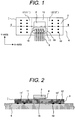
- the strain sensor chip 2 is bonded to the metal base plate 3 with a metal solder 4.
- a metalizing layer comprising three layers of Cr, Ni and Au is formed by sputtering, and a metal solder material of Sn group is vapor-deposited thereon.
- a metalizing layer comprising three layers of Cr, Ni and Au is formed on a surface of the metal base plate 3 opposed to the strain sensor chip 2.
- the strain sensor chip 2 is placed on a central part of the metal base plate 3. Further, the metal solder 4 is heated and melted to bond the strain sensor chip 2 to the metal base plate 3.
- the metalizing layer comprising three layers can be formed all over the metal base plate.
- each portion of the sensor chip circuit 21 has a parasitic capacitance 22 between itself and the object 6 to be measured. Accordingly, the potential of the sensor chip circuit 21 also varies, allowing a noise to be generated easily.
- the strain sensor chip is metal-bonded to the metal base plate, and it can be produced as a module in which a flexible circuit board wiring is connected.
- the semiconductor strain sensor of the present invention by welding the connection area of the extending member to the object to be measured, the strain can be measured. Even to an immobilized object to be measured, the semiconductor strain sensor can be attached by bringing a spot resistance welder to a work site. Moreover, in addition to the spot resistance welding, laser welding or seam welding can be employed. Since the strain sensor chip is attached to the object to be measured through the metal base plate, the risk of damaging the sensor chip or changing the characteristics by giving unnecessary strain could be reduced when mounting it.
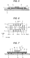
- Fig. 4 is a plan view of a semiconductor strain sensor 1 of Example 2, attached to the object to be measured.
- Fig. 5 is a sectional view taken along line V-V of Fig. 4 .
- Bolt holes 23 are formed in two overhanging members 11 and 12 of the metal base plate 3, respectively.
- the semiconductor strain sensor 1 is fixed to the object 6 to be measured with bolts 24. So long as screw holes can be formed, the screw joint is applicable to ceramics etc. to which welding cannot be performed.
- connection areas 13' and 14' of the two extending members 13 and 14 provided in the Y direction are connected to the object 6 to be measured by spot resistance welding.
- the reference numeral 19 designates a welding point.
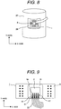
- the semiconductor strain sensor of Example 3 is also suited to torque detection.
- An example of the torque detection is shown in Fig. 8 .
- a pillar member 27 to which torque is applied is used as an object to be measured.
- a notch slot 28 is formed in a side face of the pillar member, and a semiconductor strain sensor 1 is attached to a flat bottom of the slot.
- the semiconductor strain sensor of the present embodiment is fixed to the pillar member 27 of the object to be measured by welding through four connection areas around the strain sensor chip. The strain is transmitted from the object to be measured in the X and Y directions. Therefore, shearing strain caused by torsion of the object to be measured is transmitted to the strain sensor chip 2, and the shearing strain proportional to the torque can be obtained by calculation.
- the flexible wiring board becomes unnecessary.
- assembly processes such as bonding the flexible wiring board to the metal base plate. It is a wiring draw-out structure suited to a case where there are few wirings to be drawn out.
- a side wall closer to the bonding area is so provided as to match a line on the undersurface of the metal base plate corresponding to the side of the bonding area 15.
- the groove 30 is longer than a width (a length in the Y direction) of the semiconductor sensor chip 2, and is as long as a width of the metal base plate 3.
- the side wall close to the strain sensor chip 2 of the groove 30 substantially matches a position of the side of the strain sensor chip. Therefore, a length of the protruding section 35 in the X direction is substantially the same as a length of the bonding area 15 of the strain sensor chip 2 in the X direction.
- the metal base plate 3 is made of an alloy of Fe 58-Ni 42, and it can be 14 mm long, 6 mm wide, and 0.3mm thick.
- the strain sensor chip 2 can be 2.5 mm long, 2.5mm wide, and 0.16 mm thick.
- a width lb of the groove 30 is 0.3 mm and its depth ts is 0.18 mm.
- Each of the two bonding areas 11' and 12' is 5.45 mm long and 6 mm wide.
- the protruding section 35 is 2.5 mm long and 6 mm wide.
- the strain sensor chip 2 is placed in the recess 39. Therefore, the strain sensor chip 2 is arranged in a symmetrical relationship to the protruding section 35 on the undersurface of the strain sensor chip 2, improving the symmetrical characteristic of rigidity.
Landscapes
- Physics & Mathematics (AREA)
- General Physics & Mathematics (AREA)
- Measurement Of Length, Angles, Or The Like Using Electric Or Magnetic Means (AREA)
- Pressure Sensors (AREA)
Claims (6)
- Halbleiterdehnungssensor (1), umfassend:einen Dehnungssensorchip (2), der aus einem Halbleitersubstrat hergestellt ist und ein piezoresistives Element aufweist, das auf seiner Oberseite ausgebildet ist;eine Metallbasisplatte (3) mit einem Bondingbereich (15), an den eine Unterseite des Dehnungssensorchips (2) mit einem Metall bondenden Material (4) gebondet ist, wobei die Metallbasisplatte (3) zumindest zwei Erweiterungselemente (11, 12) aufweist, die von entgegengesetzten Seiten des Bondingbereichs (15) vorstehen, wobei jedes der Erweiterungselemente (11, 12) einen zum Bondingbereich (15) entgegengesetzten Verbindungsbereich (11', 12') auf einer Unterseite der Metallbasisplatte (3) zum Anbringen des Dehnungssensorchips (2) an eine Oberfläche eines zu messenden Objekts (6) aufweist; undein Verdrahtungselement, das mit einer Vielzahl von Elektroden (16) des piezoresistiven Elements des Dehnungssensorchips (2) verbunden und nach außen gezogen ist,wobei die Metallbasisplatte (3) entlang einer Linie ausgebildet ist, die einer Seite des Bondingbereichs (15) auf der Unterseite der Metallbasisplatte entspricht, unddadurch gekennzeichnet, dass:
die Metallbasisplatte (3) ein Paar von Nuten (30) aufweist, die so lang wie oder länger als eine Länge der Seite des Bondingbereichs sind, die der Linie entspricht, entlang der die Metallbasisplatte (3) ausgebildet ist, wobei jede des Paars von Nuten (30) einen Bereich, der dem Bondingbereich (15) entspricht, von jedem der Verbindungsbereiche (11', 12') der Erweiterungselemente (11, 12) auf der Unterseite der Metallbasisplatte (3) trennt, und wobei jede des Paars von Nuten (30) sich senkrecht zu einer Dehnungsdetektionsrichtung des Dehnungssensorchips (2) erstreckt, sodass ein vorstehender Abschnitt (35) zwischen den Nuten (30) ausgebildet ist und unter dem Bondingbereich (15) angeordnet ist. - Halbleiterdehnungssensor (1) nach Anspruch 1,
wobei eine Seitenwand, die näher zum Bondingbereich (15) von Seitenwänden des Paars von Nuten (30) angeordnet ist, entlang der Linie bereitgestellt ist, die der Seite des Bondingbereichs (15) auf der Unterseite der Metallbasisplatte (3) entspricht. - Halbleiterdehnungssensor (1) nach Anspruch 1,
wobei die Metallbasisplatte (3) ein Paar von Nuten (30') in der Oberseite der Metallbasisplatte (3) aufweist, die in einer Symmetriebeziehung zu dem Paar von Nuten (30) in der Unterseite der Metallbasisplatte (3) in Bezug auf eine Ebene auf einem mittleren, dicken Teil der Metallbasisplatte (3) angeordnet sind; und
wobei der Bondingbereich (15, 39) zwischen dem Paar von Nuten (30') in der Oberseite ausgebildet ist und von der Oberseite um eine Tiefe des Paars von Nuten (30') in der Oberseite eingelassen ist. - Halbleiterdehnungssensor (1) nach Anspruch 1,
wobei das Verdrahtungselement Folgendes umfasst:eine flexible Verdrahtungsplatte (5), deren eines Ende mit einem Harz auf der Metallbasisplatte (3) angehaftet ist;Metalldrähte (17), die entsprechende Verdrahtungen der flexiblen Verdrahtungsplatte (5) mit entsprechenden der Vielzahl von Elektroden (16) des piezoresistiven Elements des Dehnungssensorchips (2) verbinden; undein Harz (18), das die Vielzahl von Elektroden (16) des piezoresistiven Elements und der Metallverdrahtungen (17) abdeckt. - Halbleiterdehnungssensor (1) nach Anspruch 1,
wobei das Verdrahtungselement Folgendes umfasst:Metallhöcker (26), die an jeder der Vielzahl von Elektroden (16) des piezoresistiven Elements des Dehnungssensorchips (2) entsprechend bereitgestellt sind;eine flexible Verdrahtungsplatte (5) mit Verdrahtungen, die mit entsprechenden der Metallhöcker (26) elektrisch verbunden sind; undein Harz, das zwischen dem Dehnungssensorchip (2) und der flexiblen Verdrahtungsplatte (5) eingefüllt ist. - Halbleiterdeformationssensor (1) nach Anspruch 1,
wobei das Verdrahtungselement Folgendes umfasst:eine Basisplattenelektrode (32), die durch einen Isolierfilm auf der Metallbasisplatte (3) ausgebildet ist;Metalldrähte (17), die die Basisplattenelektrode (32) mit der Vielzahl von Elektroden (16) des piezoresistiven Elements des Dehnungssensorchips (2) elektrisch verbinden; undein Harz, das die Vielzahl von Elektroden (16) des piezoresistiven Elements , die Metalldrähte (17) und die Basisplattenelektrode (32) abdeckt.
Applications Claiming Priority (3)
| Application Number | Priority Date | Filing Date | Title |
|---|---|---|---|
| JP2007219342A JP2009053005A (ja) | 2007-08-27 | 2007-08-27 | 半導体歪センサーおよび半導体歪センサーの取付け方法 |
| JP2007246695A JP4566227B2 (ja) | 2007-09-25 | 2007-09-25 | 半導体歪センサーおよび半導体歪センサーの取付け方法 |
| PCT/JP2008/063354 WO2009028283A1 (ja) | 2007-08-27 | 2008-07-25 | 半導体歪みセンサー |
Publications (3)
| Publication Number | Publication Date |
|---|---|
| EP2184576A1 EP2184576A1 (de) | 2010-05-12 |
| EP2184576A4 EP2184576A4 (de) | 2014-10-01 |
| EP2184576B1 true EP2184576B1 (de) | 2019-05-15 |
Family
ID=40387011
Family Applications (1)
| Application Number | Title | Priority Date | Filing Date |
|---|---|---|---|
| EP08828400.5A Active EP2184576B1 (de) | 2007-08-27 | 2008-07-25 | Halbleiterbelastungssensor |
Country Status (6)
| Country | Link |
|---|---|
| US (1) | US8438931B2 (de) |
| EP (1) | EP2184576B1 (de) |
| KR (1) | KR101151125B1 (de) |
| CN (1) | CN101802541B (de) |
| TW (1) | TW200914808A (de) |
| WO (1) | WO2009028283A1 (de) |
Families Citing this family (41)
| Publication number | Priority date | Publication date | Assignee | Title |
|---|---|---|---|---|
| WO2009003015A1 (en) | 2007-06-26 | 2008-12-31 | Swagelok Company | Apparatus and method of zero clearance connection with optional sensing function |
| CA2692327C (en) | 2007-06-26 | 2020-06-02 | Swagelok Company | Conduit connection with sensing function |
| DE102010002274A1 (de) * | 2010-02-24 | 2011-08-25 | Robert Bosch GmbH, 70469 | Vorrichtung zur Messung von Torsionen, Biegungen und dergleichen sowie entsprechendes Herstellungsverfahren |
| FR2957677B1 (fr) * | 2010-03-17 | 2012-09-28 | Commissariat Energie Atomique | Detecteur de sollicitation mecanique |
| US9121258B2 (en) | 2010-11-08 | 2015-09-01 | Baker Hughes Incorporated | Sensor on a drilling apparatus |
| US20140042566A1 (en) * | 2011-04-21 | 2014-02-13 | Hitachi, Ltd. | Mechanical quantity measuring device, semiconductor device, exfoliation detecting device, and module |
| WO2013084294A1 (ja) * | 2011-12-06 | 2013-06-13 | 株式会社日立製作所 | 力学量測定装置 |
| US9057247B2 (en) * | 2012-02-21 | 2015-06-16 | Baker Hughes Incorporated | Measurement of downhole component stress and surface conditions |
| JP5802824B2 (ja) * | 2012-03-02 | 2015-11-04 | 株式会社日立製作所 | 力学量測定装置 |
| CN104350366A (zh) * | 2012-05-25 | 2015-02-11 | 株式会社日立制作所 | 力学量测量装置 |
| US9250146B2 (en) * | 2013-02-12 | 2016-02-02 | Western New England University | Multidimensional strain gage |
| JP5975970B2 (ja) * | 2013-11-20 | 2016-08-23 | 日立オートモティブシステムズ株式会社 | 圧力センサ |
| US20150296622A1 (en) * | 2014-04-11 | 2015-10-15 | Apple Inc. | Flexible Printed Circuit With Semiconductor Strain Gauge |
| JP2015224903A (ja) * | 2014-05-26 | 2015-12-14 | 株式会社東芝 | 圧力センサ、マイクロフォン、超音波センサ、血圧センサ及びタッチパネル |
| US9887165B2 (en) | 2014-12-10 | 2018-02-06 | Stmicroelectronics S.R.L. | IC with insulating trench and related methods |
| US9726587B2 (en) * | 2015-01-30 | 2017-08-08 | Stmicroelectronics S.R.L. | Tensile stress measurement device with attachment plates and related methods |
| WO2016144723A1 (en) | 2015-03-06 | 2016-09-15 | Swagelok Company | Systems and methods for strain detection in a coupling |
| DE102015104410B4 (de) * | 2015-03-24 | 2018-09-13 | Tdk-Micronas Gmbh | Drucksensor |
| WO2016159245A1 (ja) * | 2015-03-31 | 2016-10-06 | 株式会社NejiLaw | 通電路付部材及び通電路のパターニング方法、部材変化計測方法 |
| JP6344297B2 (ja) * | 2015-04-16 | 2018-06-20 | 株式会社デンソー | 撮像装置およびそれに用いられるプリント基板 |
| CN108027290B (zh) * | 2015-09-30 | 2020-07-21 | 日立汽车系统株式会社 | 力学量测定装置 |
| KR102400529B1 (ko) * | 2015-10-26 | 2022-05-20 | 삼성전자주식회사 | 금속 케이스를 구비한 전자기기 및 이에 사용되는 금속 케이스 |
| JP2017150931A (ja) * | 2016-02-24 | 2017-08-31 | 株式会社タニタ | ひずみゲージ |
| CN105759879B (zh) * | 2016-03-21 | 2017-12-19 | 安徽科创新能源科技有限责任公司 | 一种印刷车间环境监测调控系统 |
| CN105786057B (zh) * | 2016-03-21 | 2018-01-12 | 安徽工程大学 | 印刷车间温湿度调节系统 |
| CN105843296B (zh) * | 2016-03-21 | 2018-03-20 | 安徽工程大学 | 印刷机烘箱的温控装置 |
| CN105843295B (zh) * | 2016-03-21 | 2018-02-16 | 安徽工程大学 | 冰箱温湿度检测调节装置 |
| KR102527317B1 (ko) * | 2016-08-30 | 2023-05-03 | 삼성전자주식회사 | 금속 패드가 부착된 금속 케이스를 구비한 전자기기 |
| US10203254B2 (en) * | 2016-09-12 | 2019-02-12 | Apple Inc. | Strain sensor with thermally conductive element |
| JP6692762B2 (ja) * | 2017-02-13 | 2020-05-13 | 日本電産コパル電子株式会社 | トルクセンサ |
| CN107504927B (zh) * | 2017-09-11 | 2024-04-19 | 重庆大学 | 一种基于金属薄板和压电薄膜的声表面波高温应变传感器芯片及其制备方法 |
| US10797126B2 (en) | 2018-01-29 | 2020-10-06 | Wuhan China Star Optoelectronics Semiconductor Display Technology Co., Ltd. | Display device and manufacturing method thereof, display panel |
| CN108155220B (zh) * | 2018-01-29 | 2019-08-02 | 武汉华星光电半导体显示技术有限公司 | 显示装置的制造方法 |
| IT201800003693A1 (it) | 2018-03-16 | 2019-09-16 | St Microelectronics Srl | Sensore di sforzi, sistema di monitoraggio di integrita' strutturale per costruzioni e processo di fabbricazione di un sensore di sforzi |
| WO2020008939A1 (ja) * | 2018-07-06 | 2020-01-09 | オムロン株式会社 | ひずみセンサ、および引張特性測定方法 |
| KR20200046282A (ko) | 2018-10-24 | 2020-05-07 | 삼성전자주식회사 | 집적 회로 장치 및 고 대역폭 메모리 장치 |
| DE102019129411A1 (de) * | 2019-09-12 | 2021-03-18 | Wika Alexander Wiegand Se & Co. Kg | Aufnehmerkörper mit einem Messelement und Herstellungsverfahren für einen Aufnehmerkörper |
| CN115280122B (zh) * | 2020-03-19 | 2026-04-17 | 导科国际贸易有限公司 | 扭矩传感器及机器人关节结构 |
| DE102022118489B4 (de) * | 2022-07-25 | 2024-06-06 | Schaeffler Technologies AG & Co. KG | Sensoranordnung zur Messung von mechanischen Dehnungen in einem Bauteil |
| CN117629469A (zh) * | 2022-08-12 | 2024-03-01 | 鹏鼎控股(深圳)股份有限公司 | 压力传感器模组及其制作方法 |
| EP4545925B1 (de) * | 2023-10-27 | 2025-12-10 | Bollhoff Otalu S.A.S. | Mechanisch stabilisierte, verformbare, mehrschichtige lastzelle, verfahren zur herstellung davon und bauelement in kombination damit |
Family Cites Families (21)
| Publication number | Priority date | Publication date | Assignee | Title |
|---|---|---|---|---|
| US3123788A (en) * | 1964-03-03 | Piezoresistive gage | ||
| GB1469644A (en) * | 1975-01-17 | 1977-04-06 | Welwyn Electric Ltd | Transducers |
| JPS54129889A (en) * | 1978-03-31 | 1979-10-08 | Hitachi Ltd | Strain measuring unit |
| DE3009163A1 (de) | 1980-03-10 | 1981-09-24 | Siemens AG, 1000 Berlin und 8000 München | Messwertaufnehmer fuer druck |
| US4498229A (en) * | 1982-10-04 | 1985-02-12 | Becton, Dickinson And Company | Piezoresistive transducer |
| JPS59137503A (ja) | 1983-01-20 | 1984-08-07 | 日本化薬株式会社 | 織編物の加工方法 |
| JPS59137503U (ja) * | 1983-03-04 | 1984-09-13 | 株式会社オリエンテック | 張力計用ロ−ドセル |
| JP3184704B2 (ja) * | 1993-04-30 | 2001-07-09 | キヤノン電子株式会社 | 記録装置 |
| US5575577A (en) * | 1993-04-30 | 1996-11-19 | Canon Denshi Kabushiki Kaisha | Recording apparatus having position detecting device |
| JPH0735628A (ja) | 1993-07-16 | 1995-02-07 | Kyowa Electron Instr Co Ltd | ひずみゲージ添着個所被覆構造およびその被覆方法 |
| JP3022738B2 (ja) * | 1994-11-07 | 2000-03-21 | 日本電気株式会社 | マルチチップモジュール |
| US6062088A (en) * | 1996-04-13 | 2000-05-16 | Robert Bosch Gmbh | Pressure sensor |
| JP2001264188A (ja) | 2000-03-21 | 2001-09-26 | Olympus Optical Co Ltd | 半導体歪ゲージおよび半導体歪ゲージの製造方法 |
| JP2001272287A (ja) | 2000-03-27 | 2001-10-05 | Tadahiro Kato | 歪み検出センサ |
| JP2003262548A (ja) | 2002-03-07 | 2003-09-19 | Yazaki Corp | 車両荷重測定用センサユニット |
| JP2004003886A (ja) * | 2002-05-31 | 2004-01-08 | Matsushita Electric Works Ltd | センサパッケージ |
| DE102005007643A1 (de) * | 2005-02-19 | 2006-08-31 | Assa Abloy Identification Technology Group Ab | Verfahren und Anordnung zum Kontaktieren von Halbleiterchips auf einem metallischen Substrat |
| JP4379360B2 (ja) * | 2005-03-22 | 2009-12-09 | 株式会社日立製作所 | 力学量測定装置 |
| JP4830391B2 (ja) * | 2005-07-29 | 2011-12-07 | 株式会社デンソー | センサ装置の製造方法及びセンサ装置 |
| JP2007059736A (ja) * | 2005-08-26 | 2007-03-08 | Citizen Watch Co Ltd | 圧電振動子パッケージ及びその製造方法ならびに物理量センサ |
| ATE446495T1 (de) * | 2006-05-30 | 2009-11-15 | Timken Co | Sensor für verschiebung, dehnung und kraft |
-
2008
- 2008-07-25 EP EP08828400.5A patent/EP2184576B1/de active Active
- 2008-07-25 WO PCT/JP2008/063354 patent/WO2009028283A1/ja not_active Ceased
- 2008-07-25 KR KR1020107003348A patent/KR101151125B1/ko active Active
- 2008-07-25 US US12/674,419 patent/US8438931B2/en active Active
- 2008-07-25 CN CN200880103012XA patent/CN101802541B/zh active Active
- 2008-08-13 TW TW097130822A patent/TW200914808A/zh unknown
Non-Patent Citations (1)
| Title |
|---|
| None * |
Also Published As
| Publication number | Publication date |
|---|---|
| US8438931B2 (en) | 2013-05-14 |
| KR20100049071A (ko) | 2010-05-11 |
| EP2184576A1 (de) | 2010-05-12 |
| US20110227178A1 (en) | 2011-09-22 |
| CN101802541B (zh) | 2013-08-07 |
| KR101151125B1 (ko) | 2012-06-01 |
| TW200914808A (en) | 2009-04-01 |
| EP2184576A4 (de) | 2014-10-01 |
| WO2009028283A1 (ja) | 2009-03-05 |
| CN101802541A (zh) | 2010-08-11 |
Similar Documents
| Publication | Publication Date | Title |
|---|---|---|
| EP2184576B1 (de) | Halbleiterbelastungssensor | |
| JP2009053005A (ja) | 半導体歪センサーおよび半導体歪センサーの取付け方法 | |
| EP2796830B1 (de) | Dehnungsmessvorrichtung | |
| JP5308060B2 (ja) | 半導体歪センサー | |
| EP2857816A1 (de) | Mechanische mengenmessvorrichtung | |
| EP3358326B1 (de) | Vorrichtung zur messung einer dynamischen menge | |
| JP6776152B2 (ja) | 起歪体およびその起歪体を備えた力覚センサ | |
| US6272929B1 (en) | High pressure piezoresistive transducer suitable for use in hostile environments | |
| EP3101400B1 (de) | Mechanische mengenmessvorrichtung und sensoreinheit | |
| EP3534126B1 (de) | Messvorrichtung, insbesondere eine lastmessvorrichtung | |
| US20090007696A1 (en) | Strain gauge type sensor | |
| CN110325832A (zh) | 应变体及具备该应变体的力传感器 | |
| JP2014048072A (ja) | 圧力センサモジュール | |
| JP4566227B2 (ja) | 半導体歪センサーおよび半導体歪センサーの取付け方法 | |
| JP6776151B2 (ja) | 起歪体およびその起歪体を備えた力覚センサ | |
| US6840111B2 (en) | Micromechanical component and pressure sensor having a component of this type | |
| JPH09269258A (ja) | ロードセル | |
| JP2002139389A (ja) | 荷重測定用センシング素子 | |
| KR20110059028A (ko) | 반도체 스트레인게이지형 압력센서모듈과 그 제조방법 | |
| JP2025093752A (ja) | 重量計 |
Legal Events
| Date | Code | Title | Description |
|---|---|---|---|
| PUAI | Public reference made under article 153(3) epc to a published international application that has entered the european phase |
Free format text: ORIGINAL CODE: 0009012 |
|
| 17P | Request for examination filed |
Effective date: 20100217 |
|
| AK | Designated contracting states |
Kind code of ref document: A1 Designated state(s): AT BE BG CH CY CZ DE DK EE ES FI FR GB GR HR HU IE IS IT LI LT LU LV MC MT NL NO PL PT RO SE SI SK TR |
|
| AX | Request for extension of the european patent |
Extension state: AL BA MK RS |
|
| DAX | Request for extension of the european patent (deleted) | ||
| A4 | Supplementary search report drawn up and despatched |
Effective date: 20140903 |
|
| RIC1 | Information provided on ipc code assigned before grant |
Ipc: G01B 7/16 20060101AFI20140828BHEP Ipc: G01L 1/22 20060101ALI20140828BHEP Ipc: G01L 1/18 20060101ALI20140828BHEP |
|
| STAA | Information on the status of an ep patent application or granted ep patent |
Free format text: STATUS: EXAMINATION IS IN PROGRESS |
|
| 17Q | First examination report despatched |
Effective date: 20171207 |
|
| GRAP | Despatch of communication of intention to grant a patent |
Free format text: ORIGINAL CODE: EPIDOSNIGR1 |
|
| STAA | Information on the status of an ep patent application or granted ep patent |
Free format text: STATUS: GRANT OF PATENT IS INTENDED |
|
| INTG | Intention to grant announced |
Effective date: 20190129 |
|
| GRAS | Grant fee paid |
Free format text: ORIGINAL CODE: EPIDOSNIGR3 |
|
| GRAA | (expected) grant |
Free format text: ORIGINAL CODE: 0009210 |
|
| STAA | Information on the status of an ep patent application or granted ep patent |
Free format text: STATUS: THE PATENT HAS BEEN GRANTED |
|
| AK | Designated contracting states |
Kind code of ref document: B1 Designated state(s): AT BE BG CH CY CZ DE DK EE ES FI FR GB GR HR HU IE IS IT LI LT LU LV MC MT NL NO PL PT RO SE SI SK TR |
|
| REG | Reference to a national code |
Ref country code: CH Ref legal event code: EP Ref country code: GB Ref legal event code: FG4D |
|
| REG | Reference to a national code |
Ref country code: DE Ref legal event code: R096 Ref document number: 602008060109 Country of ref document: DE |
|
| REG | Reference to a national code |
Ref country code: IE Ref legal event code: FG4D |
|
| REG | Reference to a national code |
Ref country code: NL Ref legal event code: MP Effective date: 20190515 |
|
| REG | Reference to a national code |
Ref country code: LT Ref legal event code: MG4D |
|
| PG25 | Lapsed in a contracting state [announced via postgrant information from national office to epo] |
Ref country code: ES Free format text: LAPSE BECAUSE OF FAILURE TO SUBMIT A TRANSLATION OF THE DESCRIPTION OR TO PAY THE FEE WITHIN THE PRESCRIBED TIME-LIMIT Effective date: 20190515 Ref country code: LT Free format text: LAPSE BECAUSE OF FAILURE TO SUBMIT A TRANSLATION OF THE DESCRIPTION OR TO PAY THE FEE WITHIN THE PRESCRIBED TIME-LIMIT Effective date: 20190515 Ref country code: NL Free format text: LAPSE BECAUSE OF FAILURE TO SUBMIT A TRANSLATION OF THE DESCRIPTION OR TO PAY THE FEE WITHIN THE PRESCRIBED TIME-LIMIT Effective date: 20190515 Ref country code: HR Free format text: LAPSE BECAUSE OF FAILURE TO SUBMIT A TRANSLATION OF THE DESCRIPTION OR TO PAY THE FEE WITHIN THE PRESCRIBED TIME-LIMIT Effective date: 20190515 Ref country code: NO Free format text: LAPSE BECAUSE OF FAILURE TO SUBMIT A TRANSLATION OF THE DESCRIPTION OR TO PAY THE FEE WITHIN THE PRESCRIBED TIME-LIMIT Effective date: 20190815 Ref country code: PT Free format text: LAPSE BECAUSE OF FAILURE TO SUBMIT A TRANSLATION OF THE DESCRIPTION OR TO PAY THE FEE WITHIN THE PRESCRIBED TIME-LIMIT Effective date: 20190915 Ref country code: FI Free format text: LAPSE BECAUSE OF FAILURE TO SUBMIT A TRANSLATION OF THE DESCRIPTION OR TO PAY THE FEE WITHIN THE PRESCRIBED TIME-LIMIT Effective date: 20190515 Ref country code: SE Free format text: LAPSE BECAUSE OF FAILURE TO SUBMIT A TRANSLATION OF THE DESCRIPTION OR TO PAY THE FEE WITHIN THE PRESCRIBED TIME-LIMIT Effective date: 20190515 |
|
| PG25 | Lapsed in a contracting state [announced via postgrant information from national office to epo] |
Ref country code: LV Free format text: LAPSE BECAUSE OF FAILURE TO SUBMIT A TRANSLATION OF THE DESCRIPTION OR TO PAY THE FEE WITHIN THE PRESCRIBED TIME-LIMIT Effective date: 20190515 Ref country code: GR Free format text: LAPSE BECAUSE OF FAILURE TO SUBMIT A TRANSLATION OF THE DESCRIPTION OR TO PAY THE FEE WITHIN THE PRESCRIBED TIME-LIMIT Effective date: 20190816 Ref country code: BG Free format text: LAPSE BECAUSE OF FAILURE TO SUBMIT A TRANSLATION OF THE DESCRIPTION OR TO PAY THE FEE WITHIN THE PRESCRIBED TIME-LIMIT Effective date: 20190815 |
|
| REG | Reference to a national code |
Ref country code: AT Ref legal event code: MK05 Ref document number: 1133967 Country of ref document: AT Kind code of ref document: T Effective date: 20190515 |
|
| PG25 | Lapsed in a contracting state [announced via postgrant information from national office to epo] |
Ref country code: CZ Free format text: LAPSE BECAUSE OF FAILURE TO SUBMIT A TRANSLATION OF THE DESCRIPTION OR TO PAY THE FEE WITHIN THE PRESCRIBED TIME-LIMIT Effective date: 20190515 Ref country code: RO Free format text: LAPSE BECAUSE OF FAILURE TO SUBMIT A TRANSLATION OF THE DESCRIPTION OR TO PAY THE FEE WITHIN THE PRESCRIBED TIME-LIMIT Effective date: 20190515 Ref country code: SK Free format text: LAPSE BECAUSE OF FAILURE TO SUBMIT A TRANSLATION OF THE DESCRIPTION OR TO PAY THE FEE WITHIN THE PRESCRIBED TIME-LIMIT Effective date: 20190515 Ref country code: EE Free format text: LAPSE BECAUSE OF FAILURE TO SUBMIT A TRANSLATION OF THE DESCRIPTION OR TO PAY THE FEE WITHIN THE PRESCRIBED TIME-LIMIT Effective date: 20190515 Ref country code: AT Free format text: LAPSE BECAUSE OF FAILURE TO SUBMIT A TRANSLATION OF THE DESCRIPTION OR TO PAY THE FEE WITHIN THE PRESCRIBED TIME-LIMIT Effective date: 20190515 Ref country code: DK Free format text: LAPSE BECAUSE OF FAILURE TO SUBMIT A TRANSLATION OF THE DESCRIPTION OR TO PAY THE FEE WITHIN THE PRESCRIBED TIME-LIMIT Effective date: 20190515 |
|
| REG | Reference to a national code |
Ref country code: DE Ref legal event code: R097 Ref document number: 602008060109 Country of ref document: DE |
|
| PG25 | Lapsed in a contracting state [announced via postgrant information from national office to epo] |
Ref country code: IT Free format text: LAPSE BECAUSE OF FAILURE TO SUBMIT A TRANSLATION OF THE DESCRIPTION OR TO PAY THE FEE WITHIN THE PRESCRIBED TIME-LIMIT Effective date: 20190515 Ref country code: MC Free format text: LAPSE BECAUSE OF FAILURE TO SUBMIT A TRANSLATION OF THE DESCRIPTION OR TO PAY THE FEE WITHIN THE PRESCRIBED TIME-LIMIT Effective date: 20190515 |
|
| REG | Reference to a national code |
Ref country code: CH Ref legal event code: PL |
|
| PLBE | No opposition filed within time limit |
Free format text: ORIGINAL CODE: 0009261 |
|
| STAA | Information on the status of an ep patent application or granted ep patent |
Free format text: STATUS: NO OPPOSITION FILED WITHIN TIME LIMIT |
|
| PG25 | Lapsed in a contracting state [announced via postgrant information from national office to epo] |
Ref country code: TR Free format text: LAPSE BECAUSE OF FAILURE TO SUBMIT A TRANSLATION OF THE DESCRIPTION OR TO PAY THE FEE WITHIN THE PRESCRIBED TIME-LIMIT Effective date: 20190515 |
|
| REG | Reference to a national code |
Ref country code: BE Ref legal event code: MM Effective date: 20190731 |
|
| 26N | No opposition filed |
Effective date: 20200218 |
|
| GBPC | Gb: european patent ceased through non-payment of renewal fee |
Effective date: 20190815 |
|
| PG25 | Lapsed in a contracting state [announced via postgrant information from national office to epo] |
Ref country code: PL Free format text: LAPSE BECAUSE OF FAILURE TO SUBMIT A TRANSLATION OF THE DESCRIPTION OR TO PAY THE FEE WITHIN THE PRESCRIBED TIME-LIMIT Effective date: 20190515 |
|
| PG25 | Lapsed in a contracting state [announced via postgrant information from national office to epo] |
Ref country code: SI Free format text: LAPSE BECAUSE OF FAILURE TO SUBMIT A TRANSLATION OF THE DESCRIPTION OR TO PAY THE FEE WITHIN THE PRESCRIBED TIME-LIMIT Effective date: 20190515 Ref country code: LU Free format text: LAPSE BECAUSE OF NON-PAYMENT OF DUE FEES Effective date: 20190725 Ref country code: BE Free format text: LAPSE BECAUSE OF NON-PAYMENT OF DUE FEES Effective date: 20190731 Ref country code: LI Free format text: LAPSE BECAUSE OF NON-PAYMENT OF DUE FEES Effective date: 20190731 Ref country code: CH Free format text: LAPSE BECAUSE OF NON-PAYMENT OF DUE FEES Effective date: 20190731 |
|
| PG25 | Lapsed in a contracting state [announced via postgrant information from national office to epo] |
Ref country code: FR Free format text: LAPSE BECAUSE OF NON-PAYMENT OF DUE FEES Effective date: 20190731 |
|
| PG25 | Lapsed in a contracting state [announced via postgrant information from national office to epo] |
Ref country code: IE Free format text: LAPSE BECAUSE OF NON-PAYMENT OF DUE FEES Effective date: 20190725 |
|
| PG25 | Lapsed in a contracting state [announced via postgrant information from national office to epo] |
Ref country code: GB Free format text: LAPSE BECAUSE OF NON-PAYMENT OF DUE FEES Effective date: 20190815 |
|
| PG25 | Lapsed in a contracting state [announced via postgrant information from national office to epo] |
Ref country code: CY Free format text: LAPSE BECAUSE OF FAILURE TO SUBMIT A TRANSLATION OF THE DESCRIPTION OR TO PAY THE FEE WITHIN THE PRESCRIBED TIME-LIMIT Effective date: 20190515 |
|
| PG25 | Lapsed in a contracting state [announced via postgrant information from national office to epo] |
Ref country code: IS Free format text: LAPSE BECAUSE OF FAILURE TO SUBMIT A TRANSLATION OF THE DESCRIPTION OR TO PAY THE FEE WITHIN THE PRESCRIBED TIME-LIMIT Effective date: 20190915 |
|
| PG25 | Lapsed in a contracting state [announced via postgrant information from national office to epo] |
Ref country code: MT Free format text: LAPSE BECAUSE OF FAILURE TO SUBMIT A TRANSLATION OF THE DESCRIPTION OR TO PAY THE FEE WITHIN THE PRESCRIBED TIME-LIMIT Effective date: 20190515 Ref country code: HU Free format text: LAPSE BECAUSE OF FAILURE TO SUBMIT A TRANSLATION OF THE DESCRIPTION OR TO PAY THE FEE WITHIN THE PRESCRIBED TIME-LIMIT; INVALID AB INITIO Effective date: 20080725 |
|
| PGFP | Annual fee paid to national office [announced via postgrant information from national office to epo] |
Ref country code: DE Payment date: 20250528 Year of fee payment: 18 |