EP2184758A1 - Procédé de production d'un panneau d'affichage plasma - Google Patents
Procédé de production d'un panneau d'affichage plasma Download PDFInfo
- Publication number
- EP2184758A1 EP2184758A1 EP09769855A EP09769855A EP2184758A1 EP 2184758 A1 EP2184758 A1 EP 2184758A1 EP 09769855 A EP09769855 A EP 09769855A EP 09769855 A EP09769855 A EP 09769855A EP 2184758 A1 EP2184758 A1 EP 2184758A1
- Authority
- EP
- European Patent Office
- Prior art keywords
- dielectric layer
- base film
- display panel
- plasma display
- pdp
- Prior art date
- Legal status (The legal status is an assumption and is not a legal conclusion. Google has not performed a legal analysis and makes no representation as to the accuracy of the status listed.)
- Withdrawn
Links
Images

Classifications
-
- H—ELECTRICITY
- H01—ELECTRIC ELEMENTS
- H01J—ELECTRIC DISCHARGE TUBES OR DISCHARGE LAMPS
- H01J9/00—Apparatus or processes specially adapted for the manufacture, installation, removal, maintenance of electric discharge tubes, discharge lamps, or parts thereof; Recovery of material from discharge tubes or lamps
- H01J9/02—Manufacture of electrodes or electrode systems
-
- H—ELECTRICITY
- H01—ELECTRIC ELEMENTS
- H01J—ELECTRIC DISCHARGE TUBES OR DISCHARGE LAMPS
- H01J11/00—Gas-filled discharge tubes with alternating current induction of the discharge, e.g. alternating current plasma display panels [AC-PDP]; Gas-filled discharge tubes without any main electrode inside the vessel; Gas-filled discharge tubes with at least one main electrode outside the vessel
- H01J11/10—AC-PDPs with at least one main electrode being out of contact with the plasma
- H01J11/12—AC-PDPs with at least one main electrode being out of contact with the plasma with main electrodes provided on both sides of the discharge space
-
- H—ELECTRICITY
- H01—ELECTRIC ELEMENTS
- H01J—ELECTRIC DISCHARGE TUBES OR DISCHARGE LAMPS
- H01J11/00—Gas-filled discharge tubes with alternating current induction of the discharge, e.g. alternating current plasma display panels [AC-PDP]; Gas-filled discharge tubes without any main electrode inside the vessel; Gas-filled discharge tubes with at least one main electrode outside the vessel
- H01J11/20—Constructional details
- H01J11/34—Vessels, containers or parts thereof, e.g. substrates
- H01J11/40—Layers for protecting or enhancing the electron emission, e.g. MgO layers
Definitions
- the present invention relates to a manufacturing method of a plasma display panel to be used in a display device or the like.
- a plasma display panel (hereinafter called a PDP) is capable of realizing a high definition and a large screen, and is commercially produced as a 65-inch class television of the like. Recently, the PDP is advanced in application in high definition television of more than double number of scan lines as compared with the conventional NTSC system, and in consideration of the environmental problems, the PDP free from lead content is demanded.
- the PDP is composed of a front plate and a rear plate.
- the front plate includes a glass substrate, a display electrode, a dielectric layer, and a protective layer.
- the display electrode is composed of a striped transparent electrode and a bus electrode formed on one principal surface of the glass substrate.
- the dielectric layer covers the display electrode, and functions as a capacitor.
- the protective layer is made of magnesium oxide (MgO) being formed on the dielectric layer.
- the rear plate includes a glass substrate, an address electrode, a base dielectric layer, a barrier rib, and a phosphor layer.
- the address electrode is formed in stripes on one principal surface of the glass substrate.
- the base dielectric layer covers the address electrode.
- the barrier rib is formed on the base dielectric layer.
- the phosphor layer is formed between barrier ribs, and emits light in red color, green color, and blue color.
- the front plate and the rear plate are hermetically sealed having the electrode forming side formed oppositely to each other, and the discharge space closed by the barrier ribs is packed with Ne-Xe discharge gas at a pressure of 400 Torr to 600 Torr.
- the PDP discharges by applying a video signal voltage selectively to the display electrode, and the ultraviolet ray generated by this discharge excites each color phosphor layer to emit light in red color, green color, and blue color, thereby realizing a color image display.
- Such PDP is disclosed, for example, in patent document 1.
- the role of the protective layer formed on the dielectric layer of the front plate is to protect the dielectric layer from ion impact generated by discharge, and to release the initial electrons for generating an address discharge. Protection of the dielectric layer from ion impact is very important for preventing elevation of discharge voltage. Similarly, releasing of the initial electrons for generating an address discharge is very important for preventing address discharge error which may cause flickering of the image.
- the electron discharge characteristic from the protective layer determines the image quality of the PDP, and controlling of electron discharge characteristic is extremely important.
- a manufacturing method of a plasma display panel of the present invention includes: forming a front plate including a dielectric layer formed on a substrate so as to cover a display electrode, and a protective layer formed on the dielectric layer; and forming a rear plate including address electrodes disposed oppositely to form a discharge space on the front plate and in directions intersecting with the display electrode, and barrier ribs for dividing the discharge space, wherein the protective layer of the front plate has a base film evaporated on the dielectric layer, and the base film is surface-treated, and an ink film composed of a plurality of crystal particles of metal oxide and an organic solvent is formed, and the organic solvent is removed from the ink film by vacuum drying, and a plurality of crystal particles are bonded on the base film.
- the present invention is devised in the light of this problem, and it is hence a primary object thereof to manufacture a PDP having a display performance of high definition and high luminance, and low in power consumption, at low cost.
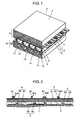
- FIG. 1 is a perspective view of structure of a PDP realized in a preferred embodiment of the present invention.
- the basic structure of the PDP is same as that of a general AC surface discharge type PDP.
- PDP 1 includes front plate 2 formed of front glass substrate 3, and rear plate 10 formed of rear glass substrate 11, disposed oppositely to each other, in which the outer circumference is hermetically sealed by a sealing member of glass frit.
- discharge space 16 is packed with a discharge gas of Ne and Xe, at a pressure of 400 Torr to 600 Torr.
- a pair of band-like display electrodes 6 composed of scan electrode 4 and sustain electrode 5 and black stripes (light shielding layers) 7 are disposed in parallel to each other in a plurality of rows.
- dielectric layer 8 functioning as a capacitor is formed for covering display electrodes 6 and light shielding layers 7.
- protective layer 9 composed of magnesium oxide (MgO) or the like is formed.
- a plurality of band-like address electrodes 12 are disposed in parallel to each other, in a direction orthogonal to scan electrodes 4 and sustain electrodes 5 of front plate 2, and they are covered with base dielectric layer 13.
- base dielectric layer 13 between address electrodes 12 barrier ribs 14 of a specified height for dividing discharge space 16 are formed.
- phosphor layers 15 for emitting light in red color, green color and blue color by ultraviolet ray are sequentially applied and formed in every one of address electrodes 12.
- Discharge cells are formed at intersecting positions of scan electrodes 4, sustain electrodes 5, and address electrodes 12, and the discharge cells having red, green and blue phosphor layers 15 arranged in a direction of display electrodes 6 become pixels for displaying a color image.
- Fig. 2 is a sectional view of structure of front plate 2 of PDP 1 realized in a preferred embodiment of the present invention, and Fig. 2 is a view of Fig. 1 inverted upside down.
- Patterns of display electrodes 6 and light shielding layers 7 formed of scan electrodes 4 and sustain electrodes 5 are formed.
- Scan electrodes 4 are formed of transparent electrodes 4a made of indium tin oxide (ITO) or tin oxide (SnO 2 ), and metal bus electrodes 4b formed on transparent electrodes 4a.
- Sustain electrodes 5 are formed of transparent electrodes 5a made of indium tin oxide (ITO) or tin oxide (SnO 2 ), and metal bus electrodes 5b formed on transparent electrodes 5a.
- Dielectric layer 8 is formed of two layers, that is, first dielectric layer 81 and second dielectric layer 82.
- Protective layer 9 is formed on second dielectric layer 82.
- First dielectric layer 81 is formed to cover all of transparent layers 4a, 5a, metal bus electrodes 4b, 5b, and light shielding layers 7 formed on front glass substrate 3.
- Second dielectric layer 82 is formed on first dielectric layer 81.
- Protective layer 9 has base film 91 made of MgO containing Al as impurities, formed on dielectric layer 8, and on this base film 91, agglomerated particles 92 agglomerating a plurality of crystal particles 92a of metal oxide MgO are scattered discretely, and are distributed almost uniformly on the entire surface.
- Fig. 3 is a sectional view showing a structure of the front plate of the PDP in the preferred embodiment of the present invention.
- Agglomerated particles 92 are formed as an agglomerating or necking group of crystal particles 92a of a specified primary particle size. They are not a bonded body having a large binding force as a solid body, but a plurality of primary particles are gathered as a group by static electricity or van der Waals force, being bonded to such a degree to become primary particles in part or in whole, by external stimulation by ultrasound or the like.
- the particle size of agglomerated particles 92 is about 1 ⁇ m, and crystal particles 92 are preferred to be polyhedral shapes having 14 facets, 12 facets, or 7 or more facets.
- Fig. 4 shows the manufacturing method of the PDP of the present invention, showing steps of forming the protective layer.
- manufacturing steps of protective film 9 are explained.
- dielectric layer 8 of a laminated structure of first dielectric layer 81 and second dielectric layer 82 is formed in dielectric layer forming step S11.
- base layer evaporating step S 12 by vacuum deposition method using a sinter of MgO containing Al as raw material, base layer 91 composed of MgO is formed on second dielectric layer 82 of dielectric layer 8.
- an excimer UV lamp of center wavelength 172 nm is emitted to the substrate surface by an integrated irradiation dose of 80 mJ or more.
- the lamp-substrate distance is set at 3 mm, by adjusting to low levels of oxygen amount and moisture amount in the treatment atmosphere by N 2 flow, damping of UV light (ultraviolet light) can be suppressed.
- emission time about 6 seconds, an integrated irradiation dose of 150 mJ will be obtained on the substrate surface.
- the surface of base film 91 of MgO is cleaned by decomposing and removing oil contaminating stains suspended in the atmosphere.
- the cleaned surface is contaminated again with the lapse of time, and base film surface treatment step S13 is preferred to be executed immediately before agglomerated particle ink layer forming step S14.
- the ink used in agglomerated particle ink layer forming step S14 is composed of agglomerated particles 92 agglomerating a plurality of MgO crystal particles 92a of metal oxide, and a solvent, and resin binder is not contained, and hence the viscosity is very low.
- Agglomerated particles 92 may be obtained by a method of heating MgO precursor, such as magnesium carbonate or magnesium hydroxide, and a plurality of primary particles are gathered into a bonded body by a relative weak force of static electricity or van der Waals force.
- MgO precursor such as magnesium carbonate or magnesium hydroxide
- the solvent has a high affinity for base film 91 of MgO or agglomerated particles 92, and it is easy to evaporate and remove in the next step of drying step S 15, and a solvent of relatively high vapor pressure of about scores of Pa at ordinary temperature is suited.
- Preferred examples of the solvent include methyl methoxy butanol, terpineol, propylene glycol, benzyl alcohol, and other organic solvents alone, or mixed solvents of them.
- the viscosity of the ink containing such solvent ranges from several units of mPaS to scores of units of mPaS.
- Means for applying such ink of agglomerated particles of very low viscosity on base film 91 in a specified film thickness includes, for example, a slit coating method.
- a slit coating method By the slit coating method, an ink film of average film thickness of 8 ⁇ m to 20 ⁇ m is uniformly formed in a specified area.
- the substrate is immediately transferred to drying step S15, and is dried at reduced pressure.
- the ink film is rapidly dried in the vacuum chamber within scores of seconds, and there is no convection of ink liquid often observed in the heating and drying process.
- agglomerated particles 92 are uniformly bonded on the surface of base film 91 without being deviated.
- a low-viscosity ink free from resin binder is applied by slit coating, and is dried in vacuum, so that agglomerated particles 92 may be bonded uniformly. Accordingly, at a low facility cost, a panel of high quality may be produced.
- a plurality of agglomerated particles can be distributed on the base film uniformly on the entire surface, and can be formed at low cost, and a PDP having a display performance of high definition and high luminance, and low in power consumption can be realized.
- the present invention is very useful for realizing a PDP having a display performance of high definition and high luminance, and low in power consumption.
Landscapes
- Engineering & Computer Science (AREA)
- Physics & Mathematics (AREA)
- Plasma & Fusion (AREA)
- Manufacturing & Machinery (AREA)
- Gas-Filled Discharge Tubes (AREA)
Applications Claiming Priority (2)
| Application Number | Priority Date | Filing Date | Title |
|---|---|---|---|
| JP2008166811A JP2010009900A (ja) | 2008-06-26 | 2008-06-26 | プラズマディスプレイパネルの製造方法 |
| PCT/JP2009/002664 WO2009157145A1 (fr) | 2008-06-26 | 2009-06-12 | Procédé de production d'un panneau d'affichage plasma |
Publications (2)
| Publication Number | Publication Date |
|---|---|
| EP2184758A1 true EP2184758A1 (fr) | 2010-05-12 |
| EP2184758A4 EP2184758A4 (fr) | 2011-08-03 |
Family
ID=41444218
Family Applications (1)
| Application Number | Title | Priority Date | Filing Date |
|---|---|---|---|
| EP09769855A Withdrawn EP2184758A4 (fr) | 2008-06-26 | 2009-06-12 | Procédé de production d'un panneau d'affichage plasma |
Country Status (6)
| Country | Link |
|---|---|
| US (1) | US20100330864A1 (fr) |
| EP (1) | EP2184758A4 (fr) |
| JP (1) | JP2010009900A (fr) |
| KR (1) | KR101150664B1 (fr) |
| CN (1) | CN101779263B (fr) |
| WO (1) | WO2009157145A1 (fr) |
Family Cites Families (15)
| Publication number | Priority date | Publication date | Assignee | Title |
|---|---|---|---|---|
| JPH08255562A (ja) * | 1995-03-17 | 1996-10-01 | Fujitsu Ltd | Pdpにおける誘電体用保護膜の形成方法 |
| US6821616B1 (en) * | 1998-12-10 | 2004-11-23 | Mitsubishi Materials Corporation | Protective thin film for FPDS, method for producing said thin film and FPDS using said thin film |
| CN100336157C (zh) * | 2000-03-31 | 2007-09-05 | 松下电器产业株式会社 | 等离子体显示面板的制造方法 |
| JP3827987B2 (ja) * | 2001-10-22 | 2006-09-27 | 旭テクノグラス株式会社 | 無鉛ガラスフリット |
| JP4056357B2 (ja) * | 2002-10-31 | 2008-03-05 | 富士通日立プラズマディスプレイ株式会社 | ガス放電パネル及びその製造方法 |
| EP1667190B1 (fr) * | 2003-09-26 | 2011-11-16 | Panasonic Corporation | Ecran plasma et son procede de fabrication |
| KR20070047075A (ko) * | 2005-11-01 | 2007-05-04 | 엘지전자 주식회사 | 플라즈마 디스플레이 패널의 보호막 |
| EP1780749A3 (fr) * | 2005-11-01 | 2009-08-12 | LG Electronics Inc. | Panneau d'affichage à plasma et procédé de fabrication |
| KR20070048017A (ko) * | 2005-11-03 | 2007-05-08 | 엘지전자 주식회사 | 플라즈마 디스플레이 패널의 보호막 |
| JP2007149384A (ja) * | 2005-11-24 | 2007-06-14 | Pioneer Electronic Corp | プラズマディスプレイパネルの製造方法、および、プラズマディスプレイパネル |
| JP4148982B2 (ja) * | 2006-05-31 | 2008-09-10 | 松下電器産業株式会社 | プラズマディスプレイパネル |
| CN101496126B (zh) * | 2006-05-31 | 2010-12-29 | 松下电器产业株式会社 | 等离子体显示面板 |
| JP2007335215A (ja) * | 2006-06-14 | 2007-12-27 | Pioneer Electronic Corp | プラズマディスプレイパネルの製造方法 |
| EP1883092A3 (fr) * | 2006-07-28 | 2009-08-05 | LG Electronics Inc. | Panneau d'affichage à plasma et son procédé de fabrication |
| KR100863960B1 (ko) * | 2006-12-01 | 2008-10-16 | 삼성에스디아이 주식회사 | 플라즈마 디스플레이 패널, 및 이의 제조 방법 |
-
2008
- 2008-06-26 JP JP2008166811A patent/JP2010009900A/ja active Pending
-
2009
- 2009-06-12 US US12/867,938 patent/US20100330864A1/en not_active Abandoned
- 2009-06-12 KR KR1020107005410A patent/KR101150664B1/ko not_active Expired - Fee Related
- 2009-06-12 CN CN200980100121.0A patent/CN101779263B/zh not_active Expired - Fee Related
- 2009-06-12 EP EP09769855A patent/EP2184758A4/fr not_active Withdrawn
- 2009-06-12 WO PCT/JP2009/002664 patent/WO2009157145A1/fr not_active Ceased
Also Published As
| Publication number | Publication date |
|---|---|
| JP2010009900A (ja) | 2010-01-14 |
| WO2009157145A1 (fr) | 2009-12-30 |
| EP2184758A4 (fr) | 2011-08-03 |
| US20100330864A1 (en) | 2010-12-30 |
| KR20100041882A (ko) | 2010-04-22 |
| KR101150664B1 (ko) | 2012-05-25 |
| CN101779263A (zh) | 2010-07-14 |
| CN101779263B (zh) | 2012-09-05 |
Similar Documents
| Publication | Publication Date | Title |
|---|---|---|
| CN101681761B (zh) | 等离子显示面板 | |
| CN101479827A (zh) | 等离子显示面板及其制造方法 | |
| JP5158265B2 (ja) | プラズマディスプレイパネル | |
| EP2184758A1 (fr) | Procédé de production d'un panneau d'affichage plasma | |
| JP2009277519A (ja) | プラズマディスプレイパネル、その製造方法および保護層形成用のペースト | |
| JP2012064424A (ja) | プラズマディスプレイパネル | |
| CN102822936A (zh) | 等离子显示面板的制造方法 | |
| US8120255B2 (en) | Plasma display panel comprising electric charge retention property | |
| CN1921061A (zh) | 等离子体显示面板及其制造方法 | |
| CN101996835B (zh) | 等离子体显示面板 | |
| EP2187422B1 (fr) | Procédé de fabrication de panneau d'affichage plasma | |
| US8198813B2 (en) | Plasma display panel | |
| KR101137605B1 (ko) | 플라즈마 디스플레이 패널의 제조 방법 | |
| EP1788608A1 (fr) | Panneau d'affichage et procédé de fabrication | |
| JP2010003423A (ja) | プラズマディスプレイパネルの製造方法 | |
| US20100255748A1 (en) | Manufacturing method of plasma display panel | |
| JP2010003422A (ja) | プラズマディスプレイパネル | |
| CN101636809B (zh) | 等离子体显示屏 | |
| JP5168422B2 (ja) | プラズマディスプレイパネルおよびプラズマディスプレイ装置 | |
| WO2011089680A1 (fr) | Procédé de fabrication d'un écran à plasma | |
| JP2010009955A (ja) | プラズマディスプレイパネルの製造方法 | |
| EP1798747A2 (fr) | Procédé de fabrication d'une couche diélectrique d'un panneau d'affichage à plasma | |
| JP2011204534A (ja) | プラズマディスプレイパネル | |
| JP2007103150A (ja) | プラズマディスプレイパネル | |
| JP2010009954A (ja) | プラズマディスプレイパネルの製造方法 |
Legal Events
| Date | Code | Title | Description |
|---|---|---|---|
| PUAI | Public reference made under article 153(3) epc to a published international application that has entered the european phase |
Free format text: ORIGINAL CODE: 0009012 |
|
| 17P | Request for examination filed |
Effective date: 20100225 |
|
| AK | Designated contracting states |
Kind code of ref document: A1 Designated state(s): AT BE BG CH CY CZ DE DK EE ES FI FR GB GR HR HU IE IS IT LI LT LU LV MC MK MT NL NO PL PT RO SE SI SK TR |
|
| AX | Request for extension of the european patent |
Extension state: AL BA RS |
|
| RIN1 | Information on inventor provided before grant (corrected) |
Inventor name: YAMASHITA, HIDEKI Inventor name: YUKI, HARUHIRO |
|
| A4 | Supplementary search report drawn up and despatched |
Effective date: 20110704 |
|
| RIC1 | Information provided on ipc code assigned before grant |
Ipc: H01J 17/04 20060101ALI20110628BHEP Ipc: H01J 17/49 20060101ALI20110628BHEP Ipc: H01J 9/02 20060101AFI20110628BHEP |
|
| DAX | Request for extension of the european patent (deleted) | ||
| STAA | Information on the status of an ep patent application or granted ep patent |
Free format text: STATUS: THE APPLICATION IS DEEMED TO BE WITHDRAWN |
|
| 18D | Application deemed to be withdrawn |
Effective date: 20140103 |