EP2184785A1 - Élément de conversion photo-électrique, corps de connexion d'élément de conversion photo-électrique et module de conversion photo-électrique - Google Patents
Élément de conversion photo-électrique, corps de connexion d'élément de conversion photo-électrique et module de conversion photo-électrique Download PDFInfo
- Publication number
- EP2184785A1 EP2184785A1 EP08791665A EP08791665A EP2184785A1 EP 2184785 A1 EP2184785 A1 EP 2184785A1 EP 08791665 A EP08791665 A EP 08791665A EP 08791665 A EP08791665 A EP 08791665A EP 2184785 A1 EP2184785 A1 EP 2184785A1
- Authority
- EP
- European Patent Office
- Prior art keywords
- photoelectric conversion
- electrode
- conversion element
- semiconductor layer
- light
- Prior art date
- Legal status (The legal status is an assumption and is not a legal conclusion. Google has not performed a legal analysis and makes no representation as to the accuracy of the status listed.)
- Withdrawn
Links
- 238000006243 chemical reaction Methods 0.000 title claims abstract description 182
- 239000004065 semiconductor Substances 0.000 claims abstract description 72
- 230000000149 penetrating effect Effects 0.000 claims abstract description 6
- 238000000034 method Methods 0.000 description 22
- 229910052782 aluminium Inorganic materials 0.000 description 20
- XAGFODPZIPBFFR-UHFFFAOYSA-N aluminium Chemical compound [Al] XAGFODPZIPBFFR-UHFFFAOYSA-N 0.000 description 20
- 239000000758 substrate Substances 0.000 description 17
- 238000004519 manufacturing process Methods 0.000 description 10
- 239000000945 filler Substances 0.000 description 8
- 239000011888 foil Substances 0.000 description 7
- 239000012535 impurity Substances 0.000 description 7
- 239000000463 material Substances 0.000 description 7
- 238000000926 separation method Methods 0.000 description 6
- 238000002955 isolation Methods 0.000 description 5
- 230000000694 effects Effects 0.000 description 4
- 239000000853 adhesive Substances 0.000 description 3
- 239000005038 ethylene vinyl acetate Substances 0.000 description 3
- 238000007747 plating Methods 0.000 description 3
- 229920001200 poly(ethylene-vinyl acetate) Polymers 0.000 description 3
- 238000007639 printing Methods 0.000 description 3
- 229910052709 silver Inorganic materials 0.000 description 3
- 239000004332 silver Substances 0.000 description 3
- 238000007740 vapor deposition Methods 0.000 description 3
- RYGMFSIKBFXOCR-UHFFFAOYSA-N Copper Chemical compound [Cu] RYGMFSIKBFXOCR-UHFFFAOYSA-N 0.000 description 2
- PXHVJJICTQNCMI-UHFFFAOYSA-N Nickel Chemical compound [Ni] PXHVJJICTQNCMI-UHFFFAOYSA-N 0.000 description 2
- KDLHZDBZIXYQEI-UHFFFAOYSA-N Palladium Chemical compound [Pd] KDLHZDBZIXYQEI-UHFFFAOYSA-N 0.000 description 2
- XUIMIQQOPSSXEZ-UHFFFAOYSA-N Silicon Chemical compound [Si] XUIMIQQOPSSXEZ-UHFFFAOYSA-N 0.000 description 2
- 230000001070 adhesive effect Effects 0.000 description 2
- 238000005260 corrosion Methods 0.000 description 2
- 238000005530 etching Methods 0.000 description 2
- 239000012212 insulator Substances 0.000 description 2
- 238000003754 machining Methods 0.000 description 2
- 229920005989 resin Polymers 0.000 description 2
- 239000011347 resin Substances 0.000 description 2
- 238000004904 shortening Methods 0.000 description 2
- 229910052710 silicon Inorganic materials 0.000 description 2
- 239000010703 silicon Substances 0.000 description 2
- BQCADISMDOOEFD-UHFFFAOYSA-N Silver Chemical compound [Ag] BQCADISMDOOEFD-UHFFFAOYSA-N 0.000 description 1
- 239000002253 acid Substances 0.000 description 1
- 239000012670 alkaline solution Substances 0.000 description 1
- 230000015572 biosynthetic process Effects 0.000 description 1
- 238000005229 chemical vapour deposition Methods 0.000 description 1
- 239000011248 coating agent Substances 0.000 description 1
- 238000000576 coating method Methods 0.000 description 1
- 229910052802 copper Inorganic materials 0.000 description 1
- 239000010949 copper Substances 0.000 description 1
- 239000013078 crystal Substances 0.000 description 1
- 229910021419 crystalline silicon Inorganic materials 0.000 description 1
- 230000002950 deficient Effects 0.000 description 1
- 238000009792 diffusion process Methods 0.000 description 1
- 239000007772 electrode material Substances 0.000 description 1
- 238000004070 electrodeposition Methods 0.000 description 1
- 230000007613 environmental effect Effects 0.000 description 1
- 239000005357 flat glass Substances 0.000 description 1
- -1 for example Substances 0.000 description 1
- 238000010438 heat treatment Methods 0.000 description 1
- 150000002500 ions Chemical class 0.000 description 1
- 239000011159 matrix material Substances 0.000 description 1
- 229910052751 metal Inorganic materials 0.000 description 1
- 239000002184 metal Substances 0.000 description 1
- 239000007769 metal material Substances 0.000 description 1
- 238000001465 metallisation Methods 0.000 description 1
- 229910052759 nickel Inorganic materials 0.000 description 1
- 229910052763 palladium Inorganic materials 0.000 description 1
- 238000000059 patterning Methods 0.000 description 1
- 238000005268 plasma chemical vapour deposition Methods 0.000 description 1
- 238000005215 recombination Methods 0.000 description 1
- 230000006798 recombination Effects 0.000 description 1
- 238000007788 roughening Methods 0.000 description 1
- 238000007650 screen-printing Methods 0.000 description 1
- 229910000679 solder Inorganic materials 0.000 description 1
- 238000005476 soldering Methods 0.000 description 1
- 230000009897 systematic effect Effects 0.000 description 1
- 239000002966 varnish Substances 0.000 description 1
Images


Classifications
-
- H—ELECTRICITY
- H10—SEMICONDUCTOR DEVICES; ELECTRIC SOLID-STATE DEVICES NOT OTHERWISE PROVIDED FOR
- H10F—INORGANIC SEMICONDUCTOR DEVICES SENSITIVE TO INFRARED RADIATION, LIGHT, ELECTROMAGNETIC RADIATION OF SHORTER WAVELENGTH OR CORPUSCULAR RADIATION
- H10F77/00—Constructional details of devices covered by this subclass
- H10F77/20—Electrodes
- H10F77/206—Electrodes for devices having potential barriers
- H10F77/211—Electrodes for devices having potential barriers for photovoltaic cells
-
- H—ELECTRICITY
- H10—SEMICONDUCTOR DEVICES; ELECTRIC SOLID-STATE DEVICES NOT OTHERWISE PROVIDED FOR
- H10F—INORGANIC SEMICONDUCTOR DEVICES SENSITIVE TO INFRARED RADIATION, LIGHT, ELECTROMAGNETIC RADIATION OF SHORTER WAVELENGTH OR CORPUSCULAR RADIATION
- H10F10/00—Individual photovoltaic cells, e.g. solar cells
- H10F10/10—Individual photovoltaic cells, e.g. solar cells having potential barriers
- H10F10/14—Photovoltaic cells having only PN homojunction potential barriers
-
- H—ELECTRICITY
- H10—SEMICONDUCTOR DEVICES; ELECTRIC SOLID-STATE DEVICES NOT OTHERWISE PROVIDED FOR
- H10F—INORGANIC SEMICONDUCTOR DEVICES SENSITIVE TO INFRARED RADIATION, LIGHT, ELECTROMAGNETIC RADIATION OF SHORTER WAVELENGTH OR CORPUSCULAR RADIATION
- H10F77/00—Constructional details of devices covered by this subclass
- H10F77/20—Electrodes
- H10F77/206—Electrodes for devices having potential barriers
- H10F77/211—Electrodes for devices having potential barriers for photovoltaic cells
- H10F77/219—Arrangements for electrodes of back-contact photovoltaic cells
- H10F77/223—Arrangements for electrodes of back-contact photovoltaic cells for metallisation wrap-through [MWT] photovoltaic cells
-
- Y—GENERAL TAGGING OF NEW TECHNOLOGICAL DEVELOPMENTS; GENERAL TAGGING OF CROSS-SECTIONAL TECHNOLOGIES SPANNING OVER SEVERAL SECTIONS OF THE IPC; TECHNICAL SUBJECTS COVERED BY FORMER USPC CROSS-REFERENCE ART COLLECTIONS [XRACs] AND DIGESTS
- Y02—TECHNOLOGIES OR APPLICATIONS FOR MITIGATION OR ADAPTATION AGAINST CLIMATE CHANGE
- Y02E—REDUCTION OF GREENHOUSE GAS [GHG] EMISSIONS, RELATED TO ENERGY GENERATION, TRANSMISSION OR DISTRIBUTION
- Y02E10/00—Energy generation through renewable energy sources
- Y02E10/50—Photovoltaic [PV] energy
- Y02E10/547—Monocrystalline silicon PV cells
Definitions
- a p-side electrode at a back side of one MWT photoelectric conversion element is connected with an n-side electrode at a back side of an adjacent MWT photoelectric conversion element by use of an interconnection foil to form a photoelectric conversion element assembly (Non-Patent Document 2).
- the interconnection foil has a patterned aluminum layer, and a surface of one part where the aluminum layer is electrically connected to each electrode at the back side of the MWT photoelectric conversion element is worked up so that an anti-corrosion layer is formed thereon, and the other part is coated with an isolating varnish. Conduction between each electrode at the back side of the MWT photoelectric conversion element and the anti-corrosion layer is made via a conductive adhesive.
- the interconnection foil Since the interconnection foil has complicated patterning, it is necessary to arrange the photoelectric conversion element on the interconnection foil with a high positioning accuracy in order to avoid trouble such as defective connection between the interconnection foil and the MWT photoelectric conversion element. Furthermore, the conductive adhesive and the production process of the interconnection foil cost more than an inter-connector.
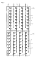
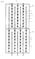
- the first electrode and the second electrode are arranged equidistantly apart from the central axis passing through the center of the photoelectric conversion element. Therefore, when two photoelectric conversion elements are arranged side by side and electrically connected to each other, and one photoelectric conversion element is turned around an axis perpendicular to the principal surface by 180 degrees, and then the central axes of each element are arranged on the same straight line, the first electrode of one photoelectric conversion element and the second electrode of the other photoelectric conversion element will necessarily be positioned on a straight line parallel to the central axes. Accordingly, the first electrode of one photoelectric conversion element and the second electrode of the other photoelectric conversion element can be connected by use of a linear inter-element wiring member. Since two photoelectric conversion elements can be connected by use of a linear inter-element wiring member according to the present invention, the period of time for this wiring process can be shortened. In addition, linear inter-element wiring members are relatively inexpensive, and therefore production costs can be reduced.
- the present invention also provides a photoelectric conversion element assembly comprising: a first photoelectric conversion element and a second photoelectric conversion element, wherein each of the first and second photoelectric conversion elements is the above-described photoelectric conversion element, the central axes of the first and second photoelectric conversion elements are arranged on the same straight line, and the first electrode of one photoelectric conversion element and the second electrode of the other photoelectric conversion element are arranged so as to be positioned on a straight line parallel to the central axes, and the first electrode of one photoelectric conversion element and the second electrode of the other photoelectric conversion element are electrically connected by use of a linear inter-element wiring member.
- the second electrode may have an asymmetrical shape with respect to the center point of the penetrating-connecting section.
- each photoelectric conversion element a distance between the first electrode and the central axis, and a distance between the penetrating-connecting section and the central axis may be different from each other.
- the present invention also provides a photoelectric conversion module comprising the above-described photoelectric conversion element assembly. The various embodiments shown herein may be combined with one another.
- FIGs. 1(a) and 1(b) are a plan view (figure of a light-receiving surface) and a back view, respectively, illustrating the configuration of the photoelectric conversion element in accordance with this embodiment; and FIG. 2 is a sectional view of the photoelectric conversion element taken along the chain line 1-1 of FIG. 1(b) .
- a photoelectric conversion element 10 of this embodiment comprises: a p-type first semiconductor layer 1 (hereinafter, referred to as "p-type layer”); a first electrode 2 arranged on the back side of the p-type layer 1 and electrically connected to the p-type layer 1; an n-type second semiconductor layer 3 (hereinafter, referred to as "n-type layer”) brought into contact with the p-type layer 1 and arranged at least in part on the light-receiving side of the p-type layer 1; a light-receiving face-side electrode 5 provided so as to be electrically connected to the n-type layer 3 on the light-receiving side of the n-type layer 3; a second electrode 7 arranged on the back side of the p-type layer 1, and electrically separated from the p-type layer 1, but electrically connected to the n-type layer 3; and a penetrating-connecting section 9 penetrating the p-type layer 1, and electrically separated from the p-type layer
- the aluminum electrode 13 is formed on the back side of the p-type layer 1 as illustrated in FIG. 3 (d) .
- the aluminum electrode 13 can be formed by printing and baking a paste material containing aluminum. On this occasion, aluminum diffuses immediately under the aluminum electrode 13 to form the high-concentration p-type layer 15 (see FIG. 4 (e) ).
- the aluminum electrode 13 is formed so as to avoid an area around the through-hole 9a (area where the second electrode 7 and the separation band 19 are to be formed in a following step).
Landscapes
- Photovoltaic Devices (AREA)
- Light Receiving Elements (AREA)
Applications Claiming Priority (2)
| Application Number | Priority Date | Filing Date | Title |
|---|---|---|---|
| JP2007226328A JP5285880B2 (ja) | 2007-08-31 | 2007-08-31 | 光電変換素子、光電変換素子接続体および光電変換モジュール |
| PCT/JP2008/063421 WO2009028287A1 (fr) | 2007-08-31 | 2008-07-25 | Élément de conversion photo-électrique, corps de connexion d'élément de conversion photo-électrique et module de conversion photo-électrique |
Publications (2)
| Publication Number | Publication Date |
|---|---|
| EP2184785A1 true EP2184785A1 (fr) | 2010-05-12 |
| EP2184785A4 EP2184785A4 (fr) | 2016-04-27 |
Family
ID=40387015
Family Applications (1)
| Application Number | Title | Priority Date | Filing Date |
|---|---|---|---|
| EP08791665.6A Withdrawn EP2184785A4 (fr) | 2007-08-31 | 2008-07-25 | Élément de conversion photo-électrique, corps de connexion d'élément de conversion photo-électrique et module de conversion photo-électrique |
Country Status (4)
| Country | Link |
|---|---|
| US (2) | US8093675B2 (fr) |
| EP (1) | EP2184785A4 (fr) |
| JP (1) | JP5285880B2 (fr) |
| WO (1) | WO2009028287A1 (fr) |
Cited By (5)
| Publication number | Priority date | Publication date | Assignee | Title |
|---|---|---|---|---|
| WO2011080340A3 (fr) * | 2010-01-04 | 2011-12-01 | Fraunhofer-Gesellschaft zur Förderung der angewandten Forschung e.V. | Pile solaire en contact électrique et procédé pour la réaliser |
| WO2012143512A1 (fr) * | 2011-04-20 | 2012-10-26 | Fraunhofer-Gesellschaft zur Förderung der angewandten Forschung e. V. | Procédé de réalisation d'une structure de contact métallique à trou métallisé dans une structure semi-conductrice et cellule solaire photovoltaïque |
| WO2014041413A1 (fr) * | 2012-09-11 | 2014-03-20 | Rec Solar Pte. Ltd. | Procédé de fabrication d'un module solaire de cellules solaires à contact arrière à l'aide de bandes de connecteur de type ruban linéaire et module solaire respectif |
| CN105405909A (zh) * | 2015-12-18 | 2016-03-16 | 英利能源(中国)有限公司 | Mwt太阳能电池 |
| CN107851674A (zh) * | 2015-07-13 | 2018-03-27 | 维斯幕达有限公司 | 用于专用导电背板的mwt类型光伏电池 |
Families Citing this family (63)
| Publication number | Priority date | Publication date | Assignee | Title |
|---|---|---|---|---|
| JP5285880B2 (ja) * | 2007-08-31 | 2013-09-11 | シャープ株式会社 | 光電変換素子、光電変換素子接続体および光電変換モジュール |
| JP2010050350A (ja) * | 2008-08-22 | 2010-03-04 | Sanyo Electric Co Ltd | 太陽電池モジュール及び太陽電池 |
| US9343490B2 (en) | 2013-08-09 | 2016-05-17 | Zena Technologies, Inc. | Nanowire structured color filter arrays and fabrication method of the same |
| US9478685B2 (en) | 2014-06-23 | 2016-10-25 | Zena Technologies, Inc. | Vertical pillar structured infrared detector and fabrication method for the same |
| US9515218B2 (en) | 2008-09-04 | 2016-12-06 | Zena Technologies, Inc. | Vertical pillar structured photovoltaic devices with mirrors and optical claddings |
| US8269985B2 (en) | 2009-05-26 | 2012-09-18 | Zena Technologies, Inc. | Determination of optimal diameters for nanowires |
| US8274039B2 (en) | 2008-11-13 | 2012-09-25 | Zena Technologies, Inc. | Vertical waveguides with various functionality on integrated circuits |
| US9000353B2 (en) | 2010-06-22 | 2015-04-07 | President And Fellows Of Harvard College | Light absorption and filtering properties of vertically oriented semiconductor nano wires |
| US8748799B2 (en) | 2010-12-14 | 2014-06-10 | Zena Technologies, Inc. | Full color single pixel including doublet or quadruplet si nanowires for image sensors |
| US9082673B2 (en) | 2009-10-05 | 2015-07-14 | Zena Technologies, Inc. | Passivated upstanding nanostructures and methods of making the same |
| US8835831B2 (en) | 2010-06-22 | 2014-09-16 | Zena Technologies, Inc. | Polarized light detecting device and fabrication methods of the same |
| US8299472B2 (en) | 2009-12-08 | 2012-10-30 | Young-June Yu | Active pixel sensor with nanowire structured photodetectors |
| US8519379B2 (en) | 2009-12-08 | 2013-08-27 | Zena Technologies, Inc. | Nanowire structured photodiode with a surrounding epitaxially grown P or N layer |
| US8889455B2 (en) | 2009-12-08 | 2014-11-18 | Zena Technologies, Inc. | Manufacturing nanowire photo-detector grown on a back-side illuminated image sensor |
| US8791470B2 (en) | 2009-10-05 | 2014-07-29 | Zena Technologies, Inc. | Nano structured LEDs |
| US8866065B2 (en) | 2010-12-13 | 2014-10-21 | Zena Technologies, Inc. | Nanowire arrays comprising fluorescent nanowires |
| US8229255B2 (en) | 2008-09-04 | 2012-07-24 | Zena Technologies, Inc. | Optical waveguides in image sensors |
| US9299866B2 (en) | 2010-12-30 | 2016-03-29 | Zena Technologies, Inc. | Nanowire array based solar energy harvesting device |
| US8735797B2 (en) | 2009-12-08 | 2014-05-27 | Zena Technologies, Inc. | Nanowire photo-detector grown on a back-side illuminated image sensor |
| US8507840B2 (en) | 2010-12-21 | 2013-08-13 | Zena Technologies, Inc. | Vertically structured passive pixel arrays and methods for fabricating the same |
| US8890271B2 (en) | 2010-06-30 | 2014-11-18 | Zena Technologies, Inc. | Silicon nitride light pipes for image sensors |
| US8546742B2 (en) | 2009-06-04 | 2013-10-01 | Zena Technologies, Inc. | Array of nanowires in a single cavity with anti-reflective coating on substrate |
| US9406709B2 (en) | 2010-06-22 | 2016-08-02 | President And Fellows Of Harvard College | Methods for fabricating and using nanowires |
| KR101072543B1 (ko) * | 2009-04-28 | 2011-10-11 | 현대중공업 주식회사 | 태양 전지의 제조 방법 |
| KR101108474B1 (ko) | 2009-05-14 | 2012-01-31 | 엘지전자 주식회사 | 태양 전지 |
| JP5388761B2 (ja) * | 2009-08-28 | 2014-01-15 | 京セラ株式会社 | 太陽電池素子の製造方法および太陽電池素子の製造装置 |
| NL2003482C2 (nl) * | 2009-09-14 | 2011-03-15 | Stichting Energie | Zonnecel en samenstel van een aantal zonnecellen. |
| US8866002B1 (en) * | 2009-11-25 | 2014-10-21 | Amkor Technology, Inc. | Through wafer via structures for concentrated photovoltaic cells |
| KR101383395B1 (ko) * | 2009-12-28 | 2014-04-09 | 현대중공업 주식회사 | 후면전극형 태양전지의 제조방법 |
| JP2011142210A (ja) * | 2010-01-07 | 2011-07-21 | Sharp Corp | 太陽電池およびその製造方法 |
| JP2011151192A (ja) * | 2010-01-21 | 2011-08-04 | Sharp Corp | 太陽電池セル、インターコネクタ付き太陽電池セルおよびその製造方法 |
| TWI453939B (zh) * | 2010-12-30 | 2014-09-21 | Au Optronics Corp | 太陽能電池及其製作方法 |
| KR101680389B1 (ko) * | 2011-03-15 | 2016-11-28 | 엘지전자 주식회사 | 태양 전지 |
| CN102800723B (zh) * | 2011-05-27 | 2015-10-21 | 苏州阿特斯阳光电力科技有限公司 | 太阳电池组件及其制造方法 |
| US9153713B2 (en) | 2011-04-02 | 2015-10-06 | Csi Cells Co., Ltd | Solar cell modules and methods of manufacturing the same |
| WO2012145864A1 (fr) * | 2011-04-29 | 2012-11-01 | 无锡尚德太阳能电力有限公司 | Cellule solaire, ensemble de cellules solaires et leurs procédés de fabrication |
| US20120279563A1 (en) * | 2011-05-02 | 2012-11-08 | Daniel Meier | Solderable interconnect apparatus for interconnecting solar cells |
| US8916410B2 (en) | 2011-05-27 | 2014-12-23 | Csi Cells Co., Ltd | Methods of manufacturing light to current converter devices |
| CN102709337A (zh) * | 2012-04-27 | 2012-10-03 | 苏州阿特斯阳光电力科技有限公司 | 一种背接触太阳能电池片、使用电池片的太阳能组件及其制备方法 |
| CN102709336A (zh) * | 2012-04-27 | 2012-10-03 | 苏州阿特斯阳光电力科技有限公司 | 一种背接触太阳能电池片的背面电极结构 |
| CN102723380A (zh) * | 2012-06-08 | 2012-10-10 | 苏州阿特斯阳光电力科技有限公司 | 一种背接触太阳能电池组件 |
| CN102810576B (zh) * | 2012-08-09 | 2015-11-18 | 晶澳(扬州)太阳能科技有限公司 | 一种双重印刷太阳能电池的电极栅线结构 |
| CN103367470A (zh) * | 2013-07-08 | 2013-10-23 | 浙江晶科能源有限公司 | 一种可直线焊接的mwt电池背面结构 |
| US9716192B2 (en) * | 2014-03-28 | 2017-07-25 | International Business Machines Corporation | Method for fabricating a photovoltaic device by uniform plating on emitter-lined through-wafer vias and interconnects |
| US10263131B2 (en) | 2014-04-07 | 2019-04-16 | Solaero Technologies Corp. | Parallel interconnection of neighboring solar cells with dual common back planes |
| US10790406B2 (en) | 2014-04-07 | 2020-09-29 | Solaero Technologies Corp. | Parallel interconnection of neighboring space-qualified solar cells via a common back plane |
| CN104282788B (zh) * | 2014-09-28 | 2017-03-22 | 苏州中来光伏新材股份有限公司 | 无主栅、高效率背接触太阳能电池模块、组件及制备工艺 |
| CN104362192A (zh) * | 2014-10-23 | 2015-02-18 | 天威新能源控股有限公司 | 一种金属环绕背接触电池及其制备方法和封装方法 |
| USD833383S1 (en) | 2016-11-16 | 2018-11-13 | Solaero Technologies Corp. | Solar cell with via |
| USD835571S1 (en) | 2016-12-08 | 2018-12-11 | Solaero Technologies Corp. | Solar cell with via |
| USD835030S1 (en) | 2016-12-12 | 2018-12-04 | Solaero Technologies Corp. | Solar cell with VIA |
| CN108878545B (zh) * | 2018-05-29 | 2020-03-10 | 江苏日托光伏科技股份有限公司 | 一种减少正极点排布的mwt电池及制备方法 |
| GB202020733D0 (en) * | 2020-12-30 | 2021-02-10 | Rec Solar Pte Ltd | Electrode assembly |
| CN113857723B (zh) * | 2021-09-28 | 2025-08-05 | 无锡奥特维科技股份有限公司 | 一种电池串焊接设备及焊接方法 |
| CN113814614B (zh) * | 2021-09-28 | 2025-09-30 | 无锡奥特维科技股份有限公司 | 一种电池串焊接设备及焊接方法 |
| US11689008B1 (en) | 2022-07-28 | 2023-06-27 | Altec Industries, Inc. | Wire tensioning system |
| US11717969B1 (en) | 2022-07-28 | 2023-08-08 | Altec Industries, Inc. | Cooperative high-capacity and high-dexterity manipulators |
| US11794359B1 (en) | 2022-07-28 | 2023-10-24 | Altec Industries, Inc. | Manual operation of a remote robot assembly |
| US11997429B2 (en) | 2022-07-28 | 2024-05-28 | Altec Industries, nc. | Reducing latency in head-mounted display for the remote operation of machinery |
| US11749978B1 (en) | 2022-07-28 | 2023-09-05 | Altec Industries, Inc. | Cross-arm phase-lifter |
| US11660750B1 (en) | 2022-07-28 | 2023-05-30 | Altec Industries, Inc. | Autonomous and semi-autonomous control of aerial robotic systems |
| US11742108B1 (en) | 2022-07-28 | 2023-08-29 | Altec Industries, Inc. | Operation and insulation techniques |
| US11697209B1 (en) | 2022-07-28 | 2023-07-11 | Altec Industries, Inc. | Coordinate mapping for motion control |
Family Cites Families (10)
| Publication number | Priority date | Publication date | Assignee | Title |
|---|---|---|---|---|
| JPH0252362A (ja) | 1988-08-15 | 1990-02-21 | Tomoegawa Paper Co Ltd | 電子写真用トナーとその製造方法 |
| JPH0711475Y2 (ja) * | 1988-09-30 | 1995-03-15 | 日本電気株式会社 | 太陽電池セル |
| AU663350B2 (en) * | 1991-12-09 | 1995-10-05 | Csg Solar Ag | Buried contact, interconnected thin film and bulk photovoltaic cells |
| US5468652A (en) | 1993-07-14 | 1995-11-21 | Sandia Corporation | Method of making a back contacted solar cell |
| JP3070489B2 (ja) * | 1996-10-09 | 2000-07-31 | トヨタ自動車株式会社 | 集光型太陽電池素子 |
| EP0881694A1 (fr) * | 1997-05-30 | 1998-12-02 | Interuniversitair Micro-Elektronica Centrum Vzw | Cellule solaire et méthode de fabrication |
| US20050172996A1 (en) | 2004-02-05 | 2005-08-11 | Advent Solar, Inc. | Contact fabrication of emitter wrap-through back contact silicon solar cells |
| US20060060238A1 (en) | 2004-02-05 | 2006-03-23 | Advent Solar, Inc. | Process and fabrication methods for emitter wrap through back contact solar cells |
| US7144751B2 (en) * | 2004-02-05 | 2006-12-05 | Advent Solar, Inc. | Back-contact solar cells and methods for fabrication |
| JP5285880B2 (ja) * | 2007-08-31 | 2013-09-11 | シャープ株式会社 | 光電変換素子、光電変換素子接続体および光電変換モジュール |
-
2007
- 2007-08-31 JP JP2007226328A patent/JP5285880B2/ja not_active Expired - Fee Related
-
2008
- 2008-07-25 EP EP08791665.6A patent/EP2184785A4/fr not_active Withdrawn
- 2008-07-25 WO PCT/JP2008/063421 patent/WO2009028287A1/fr not_active Ceased
- 2008-07-25 US US12/674,967 patent/US8093675B2/en not_active Expired - Fee Related
-
2011
- 2011-12-07 US US13/313,483 patent/US8253213B2/en not_active Expired - Fee Related
Non-Patent Citations (1)
| Title |
|---|
| VAN KERSCHAVER E. ET AL: "Record high performance modules based on screen printed MWT solar cells", CONFERENCE RECORD OF THE 29TH IEEE PHOTOVOLTAIC SPECIALISTS CONFERENCE, 2002, 19 May 2002 (2002-05-19) - 24 May 2002 (2002-05-24), pages 78 - 81, XP010666242 |
Cited By (10)
| Publication number | Priority date | Publication date | Assignee | Title |
|---|---|---|---|---|
| WO2011080340A3 (fr) * | 2010-01-04 | 2011-12-01 | Fraunhofer-Gesellschaft zur Förderung der angewandten Forschung e.V. | Pile solaire en contact électrique et procédé pour la réaliser |
| WO2012143512A1 (fr) * | 2011-04-20 | 2012-10-26 | Fraunhofer-Gesellschaft zur Förderung der angewandten Forschung e. V. | Procédé de réalisation d'une structure de contact métallique à trou métallisé dans une structure semi-conductrice et cellule solaire photovoltaïque |
| WO2014041413A1 (fr) * | 2012-09-11 | 2014-03-20 | Rec Solar Pte. Ltd. | Procédé de fabrication d'un module solaire de cellules solaires à contact arrière à l'aide de bandes de connecteur de type ruban linéaire et module solaire respectif |
| US9660121B2 (en) | 2012-09-11 | 2017-05-23 | Rec Solar Pte. Ltd. | Method for fabricating a solar module of rear contact solar cells using linear ribbon-type connector strips and respective solar module |
| US10396227B2 (en) | 2012-09-11 | 2019-08-27 | Rec Solar Pte. Ltd. | Method for fabricating a solar module of rear contact solar cells using linear ribbon-type connector strips and respective solar module |
| US11183606B2 (en) | 2012-09-11 | 2021-11-23 | Rec Solar Pte. Ltd. | Method for fabricating a solar module of rear contact solar cells using linear ribbon-type connector strips and respective solar module |
| US11715806B2 (en) | 2012-09-11 | 2023-08-01 | Rec Solar Pte. Ltd. | Method for fabricating a solar module of rear contact solar cells using linear ribbon-type connector strips and respective solar module |
| CN107851674A (zh) * | 2015-07-13 | 2018-03-27 | 维斯幕达有限公司 | 用于专用导电背板的mwt类型光伏电池 |
| CN107851674B (zh) * | 2015-07-13 | 2019-05-07 | 维斯幕达有限公司 | 用于专用导电背板的mwt类型光伏电池 |
| CN105405909A (zh) * | 2015-12-18 | 2016-03-16 | 英利能源(中国)有限公司 | Mwt太阳能电池 |
Also Published As
| Publication number | Publication date |
|---|---|
| JP2009059921A (ja) | 2009-03-19 |
| WO2009028287A1 (fr) | 2009-03-05 |
| EP2184785A4 (fr) | 2016-04-27 |
| JP5285880B2 (ja) | 2013-09-11 |
| US20120133015A1 (en) | 2012-05-31 |
| US8253213B2 (en) | 2012-08-28 |
| US20110057283A1 (en) | 2011-03-10 |
| US8093675B2 (en) | 2012-01-10 |
Similar Documents
| Publication | Publication Date | Title |
|---|---|---|
| US8093675B2 (en) | Photoelectric conversion element, photoelectric conversion element assembly and photoelectric conversion module | |
| US9691925B2 (en) | Light receiving element module and manufacturing method therefor | |
| US6803513B2 (en) | Series connected photovoltaic module and method for its manufacture | |
| CN106653912B (zh) | 一种无栅线全背接触太阳能电池组件 | |
| US8859322B2 (en) | Cell and module processing of semiconductor wafers for back-contacted solar photovoltaic module | |
| CN104282788B (zh) | 无主栅、高效率背接触太阳能电池模块、组件及制备工艺 | |
| JP5410050B2 (ja) | 太陽電池モジュール | |
| US20110108084A1 (en) | In-line flexible diode assembly for use in photovoltaic modules and method of making the same | |
| JP2010093188A (ja) | 光電変換素子、光電変換素子接続体および光電変換モジュール | |
| CN102683432A (zh) | 光伏模块 | |
| US20230044021A1 (en) | Solar cells having junctions retracted from cleaved edges | |
| JP2015207598A (ja) | 太陽電池モジュール、太陽電池およびこれに用いられる素子間接続体 | |
| CN104269454B (zh) | 无主栅、高效率背接触太阳能电池背板、组件及制备工艺 | |
| CN110047962B (zh) | Mwt太阳能电池片、电池串、电池组件及制备方法 | |
| US20210313479A1 (en) | High Power Density Solar Module and Methods of Fabrication | |
| JP2015053303A (ja) | 太陽電池セル、太陽電池モジュール、および太陽電池セルの製造方法。 | |
| WO2012128284A1 (fr) | Pile solaire du type électrode de surface arrière, son procédé de fabrication et module de piles solaires | |
| KR101153591B1 (ko) | 결정질 실리콘 태양전지의 구조 및 제조방법 | |
| WO2015072241A1 (fr) | Module élément de conversion photoélectrique et procédé de fabrication d'un module élément de conversion photoélectrique | |
| WO2013027591A1 (fr) | Cellule solaire et module solaire | |
| KR102233683B1 (ko) | 와이어를 구비한 슁글드 태양전지 패널 및 그 제조방법 | |
| KR20190056550A (ko) | Mwt형 양면수광 태양전지 및 와이어 인터커넥터를 이용한 태양전지 모듈 | |
| KR20180000070A (ko) | 후면접합 양면수광형 태양전지 및 그 제조방법 | |
| JP5409838B2 (ja) | 光電変換素子接続体および光電変換モジュール | |
| JP5406976B2 (ja) | 光電変換素子、光電変換素子接続体および光電変換モジュール |
Legal Events
| Date | Code | Title | Description |
|---|---|---|---|
| PUAI | Public reference made under article 153(3) epc to a published international application that has entered the european phase |
Free format text: ORIGINAL CODE: 0009012 |
|
| 17P | Request for examination filed |
Effective date: 20100308 |
|
| AK | Designated contracting states |
Kind code of ref document: A1 Designated state(s): AT BE BG CH CY CZ DE DK EE ES FI FR GB GR HR HU IE IS IT LI LT LU LV MC MT NL NO PL PT RO SE SI SK TR |
|
| AX | Request for extension of the european patent |
Extension state: AL BA MK RS |
|
| DAX | Request for extension of the european patent (deleted) | ||
| TPAC | Observations filed by third parties |
Free format text: ORIGINAL CODE: EPIDOSNTIPA |
|
| RA4 | Supplementary search report drawn up and despatched (corrected) |
Effective date: 20160329 |
|
| RIC1 | Information provided on ipc code assigned before grant |
Ipc: H01L 31/0224 20060101AFI20160321BHEP |
|
| STAA | Information on the status of an ep patent application or granted ep patent |
Free format text: STATUS: REQUEST FOR EXAMINATION WAS MADE |
|
| STAA | Information on the status of an ep patent application or granted ep patent |
Free format text: STATUS: THE APPLICATION IS DEEMED TO BE WITHDRAWN |
|
| 18D | Application deemed to be withdrawn |
Effective date: 20161026 |