EP2184790A1 - Leuchtdiode und diese enthaltender Lichtquellenmodul - Google Patents
Leuchtdiode und diese enthaltender Lichtquellenmodul Download PDFInfo
- Publication number
- EP2184790A1 EP2184790A1 EP09173906A EP09173906A EP2184790A1 EP 2184790 A1 EP2184790 A1 EP 2184790A1 EP 09173906 A EP09173906 A EP 09173906A EP 09173906 A EP09173906 A EP 09173906A EP 2184790 A1 EP2184790 A1 EP 2184790A1
- Authority
- EP
- European Patent Office
- Prior art keywords
- metal material
- light emitting
- emitting diode
- hole
- substrate
- Prior art date
- Legal status (The legal status is an assumption and is not a legal conclusion. Google has not performed a legal analysis and makes no representation as to the accuracy of the status listed.)
- Withdrawn
Links
Images

Classifications
-
- H—ELECTRICITY
- H10—SEMICONDUCTOR DEVICES; ELECTRIC SOLID-STATE DEVICES NOT OTHERWISE PROVIDED FOR
- H10H—INORGANIC LIGHT-EMITTING SEMICONDUCTOR DEVICES HAVING POTENTIAL BARRIERS
- H10H20/00—Individual inorganic light-emitting semiconductor devices having potential barriers, e.g. light-emitting diodes [LED]
- H10H20/80—Constructional details
- H10H20/85—Packages
- H10H20/8506—Containers
-
- F—MECHANICAL ENGINEERING; LIGHTING; HEATING; WEAPONS; BLASTING
- F21—LIGHTING
- F21K—NON-ELECTRIC LIGHT SOURCES USING LUMINESCENCE; LIGHT SOURCES USING ELECTROCHEMILUMINESCENCE; LIGHT SOURCES USING CHARGES OF COMBUSTIBLE MATERIAL; LIGHT SOURCES USING SEMICONDUCTOR DEVICES AS LIGHT-GENERATING ELEMENTS; LIGHT SOURCES NOT OTHERWISE PROVIDED FOR
- F21K9/00—Light sources using semiconductor devices as light-generating elements, e.g. using light-emitting diodes [LED] or lasers
-
- F—MECHANICAL ENGINEERING; LIGHTING; HEATING; WEAPONS; BLASTING
- F21—LIGHTING
- F21V—FUNCTIONAL FEATURES OR DETAILS OF LIGHTING DEVICES OR SYSTEMS THEREOF; STRUCTURAL COMBINATIONS OF LIGHTING DEVICES WITH OTHER ARTICLES, NOT OTHERWISE PROVIDED FOR
- F21V29/00—Protecting lighting devices from thermal damage; Cooling or heating arrangements specially adapted for lighting devices or systems
- F21V29/50—Cooling arrangements
- F21V29/70—Cooling arrangements characterised by passive heat-dissipating elements, e.g. heat-sinks
- F21V29/83—Cooling arrangements characterised by passive heat-dissipating elements, e.g. heat-sinks the elements having apertures, ducts or channels, e.g. heat radiation holes
-
- F—MECHANICAL ENGINEERING; LIGHTING; HEATING; WEAPONS; BLASTING
- F21—LIGHTING
- F21V—FUNCTIONAL FEATURES OR DETAILS OF LIGHTING DEVICES OR SYSTEMS THEREOF; STRUCTURAL COMBINATIONS OF LIGHTING DEVICES WITH OTHER ARTICLES, NOT OTHERWISE PROVIDED FOR
- F21V29/00—Protecting lighting devices from thermal damage; Cooling or heating arrangements specially adapted for lighting devices or systems
- F21V29/85—Protecting lighting devices from thermal damage; Cooling or heating arrangements specially adapted for lighting devices or systems characterised by the material
-
- H—ELECTRICITY
- H10—SEMICONDUCTOR DEVICES; ELECTRIC SOLID-STATE DEVICES NOT OTHERWISE PROVIDED FOR
- H10H—INORGANIC LIGHT-EMITTING SEMICONDUCTOR DEVICES HAVING POTENTIAL BARRIERS
- H10H20/00—Individual inorganic light-emitting semiconductor devices having potential barriers, e.g. light-emitting diodes [LED]
- H10H20/80—Constructional details
- H10H20/85—Packages
- H10H20/858—Means for heat extraction or cooling
- H10H20/8582—Means for heat extraction or cooling characterised by their shape
-
- F—MECHANICAL ENGINEERING; LIGHTING; HEATING; WEAPONS; BLASTING
- F21—LIGHTING
- F21Y—INDEXING SCHEME ASSOCIATED WITH SUBCLASSES F21K, F21L, F21S and F21V, RELATING TO THE FORM OR THE KIND OF THE LIGHT SOURCES OR OF THE COLOUR OF THE LIGHT EMITTED
- F21Y2115/00—Light-generating elements of semiconductor light sources
- F21Y2115/10—Light-emitting diodes [LED]
-
- H—ELECTRICITY
- H05—ELECTRIC TECHNIQUES NOT OTHERWISE PROVIDED FOR
- H05K—PRINTED CIRCUITS; CASINGS OR CONSTRUCTIONAL DETAILS OF ELECTRIC APPARATUS; MANUFACTURE OF ASSEMBLAGES OF ELECTRICAL COMPONENTS
- H05K1/00—Printed circuits
- H05K1/02—Details
- H05K1/0201—Thermal arrangements, e.g. for cooling, heating or preventing overheating
- H05K1/0203—Cooling of mounted components
- H05K1/0204—Cooling of mounted components using means for thermal conduction connection in the thickness direction of the substrate
- H05K1/0206—Cooling of mounted components using means for thermal conduction connection in the thickness direction of the substrate by printed thermal vias
-
- H—ELECTRICITY
- H10—SEMICONDUCTOR DEVICES; ELECTRIC SOLID-STATE DEVICES NOT OTHERWISE PROVIDED FOR
- H10H—INORGANIC LIGHT-EMITTING SEMICONDUCTOR DEVICES HAVING POTENTIAL BARRIERS
- H10H20/00—Individual inorganic light-emitting semiconductor devices having potential barriers, e.g. light-emitting diodes [LED]
- H10H20/80—Constructional details
- H10H20/85—Packages
- H10H20/857—Interconnections, e.g. lead-frames, bond wires or solder balls
-
- H—ELECTRICITY
- H10—SEMICONDUCTOR DEVICES; ELECTRIC SOLID-STATE DEVICES NOT OTHERWISE PROVIDED FOR
- H10W—GENERIC PACKAGES, INTERCONNECTIONS, CONNECTORS OR OTHER CONSTRUCTIONAL DETAILS OF DEVICES COVERED BY CLASS H10
- H10W72/00—Interconnections or connectors in packages
- H10W72/50—Bond wires
-
- H—ELECTRICITY
- H10—SEMICONDUCTOR DEVICES; ELECTRIC SOLID-STATE DEVICES NOT OTHERWISE PROVIDED FOR
- H10W—GENERIC PACKAGES, INTERCONNECTIONS, CONNECTORS OR OTHER CONSTRUCTIONAL DETAILS OF DEVICES COVERED BY CLASS H10
- H10W74/00—Encapsulations, e.g. protective coatings
Definitions
- the present invention relates generally to light emitting diodes (LEDs) and particularly to an LED having high heat transfer efficiency and a light source module using the LED.
- LEDs light emitting diodes
- LED light emitting diodes
- CCFL cold cathode fluorescent lamps
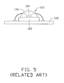
- a typical LED 100 includes a substrate 102, an LED chip 104 disposed on the substrate 102, and an encapsulant material 106 covering the LED chip 104.
- the LED 100 is mounted to a circuit board 108.
- the LED chip 104 emits light and generates heat therefrom.
- the light passes through the encapsulant material 106 to illuminate.
- the heat is transferred to the circuit board 108 by the substrate 102, and dissipated in the air.
- a conventional material of the substrate 102 such as fiberglass generally has high thermal resistance. Heat transfer efficiency of the LED 100 is limited due to the high thermal resistance of the substrate 102.
- the heat from the LED 100 can not be dissipated quickly, and light intensity of the LED 10 may be attenuated gradually, shortening life thereof.
- an illumination device includes a substrate, a metal material and a light emitting diode chip.
- the substrate has a first surface and a first through hole defined in the first surface.
- the first through hole is filled with the metal material.
- the light emitting diode chip is mounted on the first surface contacting the metal material in the first through hole.
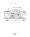
- FIG. 1 is cross-section of a LED, in accordance with a first embodiment.
- FIG 2 is cross-section of a LED, in accordance with a second embodiment.
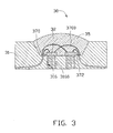
- FIG. 3 is cross-section of a LED, in accordance with a third embodiment.
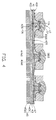
- FIG. 4 is cross-section of a light source module according to a fourth embodiment using a plurality of LEDs in FIG. 1 .
- FIG. 5 is a schematic view of a typical LED.
- the LED 10 includes a substrate 11, an LED chip 12, and an encapsulant material 15.
- the substrate 11 supports the LED chip 12 and the encapsulant material 15 thereon, and may be made of ceramic material, which has good electrical insulation property.
- the ceramic material can be comprised of a mixture of silicon oxide (SiO 2 ) and aluminum oxide (Al 2 O 3 ).
- the substrate 11 includes a first surface 110 and a second surface 112 surrounding the first surface 110. The second surface 112 connects with the first surface 110 to cooperatively form an accommodating space 114 for receiving the LED chip 12.
- the substrate 11 has at least one first through hole 116 defined in the first surface 110 to communicate with the accommodating space 114. In the first embodiment, one first through hole 116 is defined and filled with a first thermally conductive material 1160.
- the first thermally conductive material 1160 may be metal material, such as copper, silver, etc.
- the LED chip 12 is mounted directly on the first surface 110 of the substrate 11 to contact the first thermally conductive material 1160 in the first through hole 116. Thereby the first thermally conductive material 1160 in the first through hole 116, together with the substrate 11 can transfer the heat generated by the LED chip 12 to the outside of the LED 10. In this manner, the LED chip 12 may operate continually within an acceptable temperature range to achieve stable optical performance, and the brightness and the luminous efficiency of the LED 10 are stably maintained.
- the first thermally conductive material 1160 in this embodiment is silver, which has a high heat transfer coefficient of about 430W/mk, and has anti-oxidation characteristic.
- the ceramic material of the substrate 11 has a thermal expansivity in a range from about 5.8 ppm/°C to about 6.2 ppm/°C
- the first thermally conductive material 1160 has a thermal expansivity in a range from about 7 ppm/°C to about 10 ppm/°C, which is near to that of the ceramic material.
- the LED 10 further includes a positive electrode 170 and a negative electrode 172 formed on the first surface 110.
- the LED chip 12 is electrically connected to the positive electrode 170 and the negative electrode 172 each through a first wire 1700, and each first wire 1700 is further connected to an exterior power supply (not shown) having an anode and a cathode through a second wire 1800 (encapsulated in the substrate 11 in FIG. 1 ). Thereby, electric current can be applied to the LED chip 12.
- the encapsulant material 15 is disposed on the first surface 110 of the substrate 11 to fill the accommodating space 114 and cover the LED chip 12, as well as the positive electrode 170 and the negative electrode 172.
- the encapsulant material 15 is configured for optically adjusting (e.g., diverging or converging) a direction of the light emitted from the LED chip 12, thus adjusting an illuminating scope of the LED 10.
- the encapsulant material 15 protects the LED chip 12 from contaminants.
- the encapsulant material 15 is arc-shaped in this embodiment.
- an LED 20, in accordance with a second embodiment, is shown.
- the LED 20 is similar to the LED 10 in the first embodiment except that a substrate 21 has four first through holes 216 defined in a first surface 210 thereof.
- the four first through holes 216 are parallel with one another, and each is filled with a first thermally conductive material 2160 contacting the LED chip 22.
- FIG. 3 illustrates an LED 30 according to a third embodiment.
- the LED 30 is similar to the LED 20 in the second embodiment except that the LED 30 includes two LED chips 32 disposed on a substrate 31 and adjacent to one another.
- the two LED chips 32 are each electrically connected to a positive electrode 370 and a negative electrode 372 through a first wire 3700.
- the substrate 31 has six first through holes 316 defined in a first surface 310 thereof.
- Each LED chip 22 contacts a thermally conductive material 3160 through several of the first through holes 316, for example, through three first through holes 316.
- the light source module 40 includes a circuit board 41, a plurality of LEDs 10 mounted on the circuit board 41, and a heat dissipation plate 43 contacting the circuit board 41.
- the LEDs 10 according to the fourth embodiment all have a same structure as the LED 10 in the first embodiment. Therefore, for the purpose of brevity, the LEDs 10 in the fourth embodiment are not further described herein with the understanding that like reference numbers of the LED 10 in the first embodiment refer to like parts in the LEDs 10 in the fourth embodiment.
- the LEDs 10 in the fourth embodiment are used as a light source for illumination. In alternative embodiments, the LEDs in the fourth embodiment can be the LEDs 20 from the second embodiment and/or the LEDs 30 from the third embodiment.
- the circuit board 41 can be a ceramic circuit board, or a fiberglass circuit board (FR4).
- the circuit board 41 includes a third surface 410 and an opposite fourth surface 412.
- the LEDs 10 are arranged on the third surface 410 and electrically coupled to the circuit board 41 by connecting the second wires 1800 to the circuit board 41 (not shown).
- the circuit board 41 has a plurality of second through holes 416 defined in the third surface 410 corresponding to the first through holes 116.
- Each second through hole 416 is filled with a second thermally conductive material 4160 contacting the first thermally conductive material 1160 in the corresponding first through hole 116.
- the heat dissipation plate 43 is coupled to the circuit board 41 through a bonding sheet 42.
- the bonding sheet 42 may be an insulated adhesive layer coated between the fourth surface 412 and the heat dissipation plate 43, and has a surface 420 coinciding with the fourth surface 412.
- the bonding sheet 42 has a plurality of third through holes 426 defined in the surface 420 corresponding to the second through holes 416. Each third through hole 426 is filled with a third thermally conductive material 4260 contacting the second thermally conductive material 4160 in the corresponding second through hole 416, and the heat dissipation plate 43.
- the first, the second, and the third thermally conductive materials 1160, 4160 and 4260 each can be metal material with high thermal conductivity, such as silver, silver alloy, or others.
- the heat dissipation plate 43 can be made of metal, such as copper, aluminum, or others. In operation, heat from each LED 10 can be transferred in sequence from the first thermally conductive material 1160, the corresponding second thermally conductive material 4160, and the corresponding third thermally conductive material 4260 to the heat dissipation plate 43. The heat then can be dissipated efficiently by the heat dissipation plate 43 to the air. It is noted, that a diameter of each second through hole 416 is larger than that of the corresponding first through hole 116.
- each first through hole 116 completely contacts the second thermally conductive material 4160 in the corresponding second through holes 416.
- the heat may be fully transferred from the first thermally conductive material 1160 to the second thermally conductive material 4160.
- a diameter of each third through hole 426 is preferably larger than that of the corresponding second through hole 416.
- the heat may be fully transferred from the second thermally conductive material 4160 to the third thermally conductive material 4260.
- the light source module 40 can further include a heat dissipation device 45 to enhance heat dissipation efficiency.
- the heat dissipation device 45 may include a base 450 contacting an opposite side of the heat dissipation plate 43 to bonding sheet 42, and a plurality of fins 452 extending from the base 450. Heat can be further transferred from the heat dissipation plate 43 to the fins 452 through the base 450. The fins 452 increase surface area contacting the air. Thus, if there is a need, more heat can be dissipated to the air.
Landscapes
- Engineering & Computer Science (AREA)
- General Engineering & Computer Science (AREA)
- Physics & Mathematics (AREA)
- Microelectronics & Electronic Packaging (AREA)
- Optics & Photonics (AREA)
- Led Device Packages (AREA)
Applications Claiming Priority (1)
| Application Number | Priority Date | Filing Date | Title |
|---|---|---|---|
| CN200810305465A CN101740678A (zh) | 2008-11-10 | 2008-11-10 | 固态发光元件及光源模组 |
Publications (1)
| Publication Number | Publication Date |
|---|---|
| EP2184790A1 true EP2184790A1 (de) | 2010-05-12 |
Family
ID=41728483
Family Applications (1)
| Application Number | Title | Priority Date | Filing Date |
|---|---|---|---|
| EP09173906A Withdrawn EP2184790A1 (de) | 2008-11-10 | 2009-10-23 | Leuchtdiode und diese enthaltender Lichtquellenmodul |
Country Status (3)
| Country | Link |
|---|---|
| US (1) | US20100117113A1 (de) |
| EP (1) | EP2184790A1 (de) |
| CN (1) | CN101740678A (de) |
Cited By (2)
| Publication number | Priority date | Publication date | Assignee | Title |
|---|---|---|---|---|
| EP2388812A3 (de) * | 2010-05-17 | 2012-10-10 | Sunonwealth Electric Machine Industry Co., Ltd. | Wärmeableitende Anordnung |
| US9209619B2 (en) | 2011-10-28 | 2015-12-08 | Epcos Ag | ESD protection component and component comprising an ESD protection component and an LED |
Families Citing this family (6)
| Publication number | Priority date | Publication date | Assignee | Title |
|---|---|---|---|---|
| KR20100094246A (ko) * | 2009-02-18 | 2010-08-26 | 엘지이노텍 주식회사 | 발광소자 패키지 및 그 제조방법 |
| US8519409B2 (en) * | 2010-11-15 | 2013-08-27 | Taiwan Semiconductor Manufacturing Company, Ltd. | Light emitting diode components integrated with thermoelectric devices |
| TWI550920B (zh) * | 2012-12-13 | 2016-09-21 | 鴻海精密工業股份有限公司 | 發光二極體 |
| CN103872233A (zh) * | 2012-12-14 | 2014-06-18 | 鸿富锦精密工业(深圳)有限公司 | 发光二极管 |
| JP6533066B2 (ja) * | 2015-02-18 | 2019-06-19 | ローム株式会社 | 電子装置 |
| CN118248821B (zh) * | 2024-04-02 | 2024-10-01 | 安徽泓冠光电科技有限公司 | 一种空腔导热式发光二极管 |
Citations (6)
| Publication number | Priority date | Publication date | Assignee | Title |
|---|---|---|---|---|
| EP0027825A1 (de) * | 1979-04-18 | 1981-05-06 | Fujitsu Limited | Keramikbasis |
| US20040222433A1 (en) * | 2003-05-05 | 2004-11-11 | Lamina Ceramics | Light emitting diodes packaged for high temperature operation |
| WO2005001943A1 (en) * | 2003-06-30 | 2005-01-06 | Koninklijke Philips Electronics N.V. | Light-emitting diode thermal management system |
| US20060186535A1 (en) * | 2005-02-23 | 2006-08-24 | Visteon Global Technologies, Inc. | Semi-conductor die mount assembly |
| EP1760784A2 (de) * | 2005-09-01 | 2007-03-07 | E.I.Du pont de nemours and company | Keramikband-Verbundswerkstoffe gesintert bei niedriger Temperatur, Leuchtdiodenmodule, Beleuchtungsvorrichtungen und entsprechende Herstellungsverfahren |
| US20070235746A1 (en) * | 2006-01-26 | 2007-10-11 | Kazuma Mitsuyama | Light emitting diode package and light emitting diode |
Family Cites Families (7)
| Publication number | Priority date | Publication date | Assignee | Title |
|---|---|---|---|---|
| US4301324A (en) * | 1978-02-06 | 1981-11-17 | International Business Machines Corporation | Glass-ceramic structures and sintered multilayer substrates thereof with circuit patterns of gold, silver or copper |
| US4943470A (en) * | 1985-01-11 | 1990-07-24 | Ngk Spark Plug Co., Ltd. | Ceramic substrate for electrical devices |
| EP1605524B1 (de) * | 2003-03-18 | 2010-06-30 | Sumitomo Electric Industries, Ltd. | Gehäuse für lichtemittierendes element und verwendendes halbleiterbauteil |
| JP2005197659A (ja) * | 2003-12-08 | 2005-07-21 | Sony Corp | 光学装置及び画像生成装置 |
| US20080043444A1 (en) * | 2004-04-27 | 2008-02-21 | Kyocera Corporation | Wiring Board for Light-Emitting Element |
| JP2008034622A (ja) * | 2006-07-28 | 2008-02-14 | Sharp Corp | 半導体発光素子アセンブリ |
| US7625104B2 (en) * | 2007-12-13 | 2009-12-01 | Philips Lumileds Lighting Company, Llc | Light emitting diode for mounting to a heat sink |
-
2008
- 2008-11-10 CN CN200810305465A patent/CN101740678A/zh active Pending
-
2009
- 2009-06-20 US US12/488,551 patent/US20100117113A1/en not_active Abandoned
- 2009-10-23 EP EP09173906A patent/EP2184790A1/de not_active Withdrawn
Patent Citations (6)
| Publication number | Priority date | Publication date | Assignee | Title |
|---|---|---|---|---|
| EP0027825A1 (de) * | 1979-04-18 | 1981-05-06 | Fujitsu Limited | Keramikbasis |
| US20040222433A1 (en) * | 2003-05-05 | 2004-11-11 | Lamina Ceramics | Light emitting diodes packaged for high temperature operation |
| WO2005001943A1 (en) * | 2003-06-30 | 2005-01-06 | Koninklijke Philips Electronics N.V. | Light-emitting diode thermal management system |
| US20060186535A1 (en) * | 2005-02-23 | 2006-08-24 | Visteon Global Technologies, Inc. | Semi-conductor die mount assembly |
| EP1760784A2 (de) * | 2005-09-01 | 2007-03-07 | E.I.Du pont de nemours and company | Keramikband-Verbundswerkstoffe gesintert bei niedriger Temperatur, Leuchtdiodenmodule, Beleuchtungsvorrichtungen und entsprechende Herstellungsverfahren |
| US20070235746A1 (en) * | 2006-01-26 | 2007-10-11 | Kazuma Mitsuyama | Light emitting diode package and light emitting diode |
Cited By (2)
| Publication number | Priority date | Publication date | Assignee | Title |
|---|---|---|---|---|
| EP2388812A3 (de) * | 2010-05-17 | 2012-10-10 | Sunonwealth Electric Machine Industry Co., Ltd. | Wärmeableitende Anordnung |
| US9209619B2 (en) | 2011-10-28 | 2015-12-08 | Epcos Ag | ESD protection component and component comprising an ESD protection component and an LED |
Also Published As
| Publication number | Publication date |
|---|---|
| CN101740678A (zh) | 2010-06-16 |
| US20100117113A1 (en) | 2010-05-13 |
Similar Documents
| Publication | Publication Date | Title |
|---|---|---|
| US7919789B2 (en) | Lateral light-emitting diode backlight module | |
| JP5101578B2 (ja) | 発光ダイオード照明装置 | |
| TWI476347B (zh) | 照明裝置(三) | |
| US7572033B2 (en) | Light source module with high heat-dissipation efficiency | |
| US7192163B2 (en) | Light-emitting unit with enhanced thermal dissipation and method for fabricating the same | |
| US8067782B2 (en) | LED package and light source device using same | |
| US20110175512A1 (en) | Light emitting diode and light source module having same | |
| US7789535B2 (en) | Light source device with high heat-dissipation efficiency | |
| JP2008293966A (ja) | 発光ダイオードランプ | |
| US20040264195A1 (en) | Led light source having a heat sink | |
| US20100117113A1 (en) | Light emitting diode and light source module having same | |
| JP4880358B2 (ja) | 光源用基板及びこれを用いた照明装置 | |
| US20100163890A1 (en) | Led lighting device | |
| US20070081342A1 (en) | System and method for mounting a light emitting diode to a printed circuit board | |
| US20110175511A1 (en) | Light emitting diode and light source module having same | |
| US20100135015A1 (en) | Led illumination device | |
| US7838986B2 (en) | Illumination device | |
| CN103154607A (zh) | 提高了散热特性的高光度led光源构造体 | |
| KR20100133286A (ko) | 방열구조를 구비한 엘이디 조명기구 | |
| US20070291489A1 (en) | Light source device and method of making the device | |
| KR100873458B1 (ko) | 조명용 led 모듈 | |
| KR100615404B1 (ko) | 발광다이오드 모듈 | |
| US8419237B2 (en) | Heat sink and light emitting diode lamp | |
| KR20110129614A (ko) | 고효율의 열방출이 가능한 전기전자 장치 및 led 발광 장치 | |
| EP2251915A1 (de) | Licht emittierende Diode und Lichtquellenmodul damit |
Legal Events
| Date | Code | Title | Description |
|---|---|---|---|
| PUAI | Public reference made under article 153(3) epc to a published international application that has entered the european phase |
Free format text: ORIGINAL CODE: 0009012 |
|
| AK | Designated contracting states |
Kind code of ref document: A1 Designated state(s): AT BE BG CH CY CZ DE DK EE ES FI FR GB GR HR HU IE IS IT LI LT LU LV MC MK MT NL NO PL PT RO SE SI SK SM TR |
|
| AX | Request for extension of the european patent |
Extension state: AL BA RS |
|
| STAA | Information on the status of an ep patent application or granted ep patent |
Free format text: STATUS: THE APPLICATION IS DEEMED TO BE WITHDRAWN |
|
| 18D | Application deemed to be withdrawn |
Effective date: 20101012 |