EP2184802A1 - Nicht-reziproke schaltvorrichtung - Google Patents
Nicht-reziproke schaltvorrichtung Download PDFInfo
- Publication number
- EP2184802A1 EP2184802A1 EP07830947A EP07830947A EP2184802A1 EP 2184802 A1 EP2184802 A1 EP 2184802A1 EP 07830947 A EP07830947 A EP 07830947A EP 07830947 A EP07830947 A EP 07830947A EP 2184802 A1 EP2184802 A1 EP 2184802A1
- Authority
- EP
- European Patent Office
- Prior art keywords
- central electrode
- ferrite
- port
- capacitor
- output port
- Prior art date
- Legal status (The legal status is an assumption and is not a legal conclusion. Google has not performed a legal analysis and makes no representation as to the accuracy of the status listed.)
- Granted
Links
Images



Classifications
-
- H—ELECTRICITY
- H01—ELECTRIC ELEMENTS
- H01P—WAVEGUIDES; RESONATORS, LINES, OR OTHER DEVICES OF THE WAVEGUIDE TYPE
- H01P1/00—Auxiliary devices
- H01P1/32—Non-reciprocal transmission devices
- H01P1/36—Isolators
-
- H—ELECTRICITY
- H01—ELECTRIC ELEMENTS
- H01P—WAVEGUIDES; RESONATORS, LINES, OR OTHER DEVICES OF THE WAVEGUIDE TYPE
- H01P1/00—Auxiliary devices
- H01P1/32—Non-reciprocal transmission devices
- H01P1/38—Circulators
- H01P1/383—Junction circulators, e.g. Y-circulators
- H01P1/387—Strip line circulators
Definitions
- the present invention relates to nonreciprocal circuit devices, and more particularly, relates to a nonreciprocal circuit device such as an isolator or a circulator used in microwave bands.
- nonreciprocal circuit devices such as isolators or circulators transmit signals in a predetermined direction and forbid transmission of the signals in an opposite direction.
- isolators are employed in transmission circuit sections for mobile communication devices such as automobile telephones and cellular phones.
- Patent Document 1 discloses such a nonreciprocal circuit device as a two-port isolator in which a first central electrode and a second central electrode are arranged on a surface of a ferrite so as to intersect each other in an isolated manner, a resistor is connected between one end of the first central electrode connected to an input port at the other end thereof and one end of the second central electrode connected to an output port at the other end thereof, and an inductor is connected to the resistor in series.
- the two-port isolator realizes an insertion loss bandwidth and an isolation bandwidth of practical use by setting intersection angles of the first and second central electrodes in a range from 40 to 80 degrees.
- the inductor is provided for compensating for deviation of phase caused due to shift of the intersection angles from 90 degrees.
- a large insertion loss bandwidth causes a small isolation bandwidth
- a large isolation bandwidth causes a small insertion loss bandwidth.
- Patent Document 2 discloses with reference to Figs. 6 and 7 thereof a two-port isolator in which first and second central electrodes are arranged on a ferrite so as to intersect each other in an insulated manner, one end of the first central electrode is connected to an input port, the other end of the first central electrode and one end of the second central electrode are connected to an output port, the other end of the second central electrode is connected to a ground port, and matching capacitors and a resistor are connected between the input port and the output port in parallel.
- the two-port isolator has an advantage in that insertion loss is considerably reduced, there is a demand for a larger isolation bandwidth.
- a nonreciprocal circuit device including permanent magnets, a ferrite to which DC magnetic fields are applied using the permanent magnets, and first and second central electrodes arranged on the ferrite so as to intersect each other and so as to be insulated from each other.
- the first central electrode has a first end electrically connected to an input port and a second end electrically connected to an output port.
- the second central electrode has a first end electrically connected to the output port and a second end electrically connected to a ground port.
- a first matching capacitor is electrically connected between the input port and the output port.
- a second matching capacitor is electrically connected between the output port and the ground port.
- a resistor is electrically connected between the input port and the output port.
- An inductor and a capacitor included in an LC series resonance circuit are electrically connected between the input port and the output port so as to be parallel to the first central electrode and so as to be connected to the resistor in series.
- the inductor and the capacitor included in the LC series resonance circuit are electrically connected between the input port and the output port so as to be connected to the first electrode in parallel and connected to the resistor in series. Accordingly, when high-frequency current is supplied to the output port, broadband matching is performed due to impedance characteristics of the resistor R1 and the LC series resonance circuit, and accordingly, an isolation characteristic is improved.
- high-frequency current is supplied from the input port to the output port, a large amount of high-frequency current is supplied to the second central electrode whereas a negligible amount of high-frequency current is supplied to the first central electrode and the resistor. Therefore, although the LC series resonance circuit is additionally provided, loss due to the presence of the LC series resonance circuit is negligible. Accordingly, the insertion loss does not increase.
- an inductor and a capacitor included in an LC series resonance circuit are electrically connected between an input port and an output port so as to be connected to a first central electrode in parallel and connected to a resistor in series, an isolation characteristic is improved while an insertion loss characteristic is maintained.
- Fig. 1 is a diagram illustrating an equivalent circuit of a two-port isolator serving as a nonreciprocal circuit device according to a first embodiment of the present invention.
- the two-port isolator serving as a lumped-parameter isolator is configured such that a first central electrode 35 serving as an inductor L1 and a second central electrode 36 serving as an inductor L2 are arranged so as to intersect each other and so that the first central electrode 35 and the second central electrode 36 are insulated from each other.
- a first end of the first central electrode 35 is connected through a matching capacitor Cs1 to an input port P1.
- a second end of the first central electrode 35 and one end of the second central electrode 36 are connected through a capacitor Cs2 to an output port P2.
- the other end of the second central electrode 36 is connected to a ground port P3.
- a matching capacitor C1 is connected between the input port P1 and the output port P2 so as to be parallel to the first central electrode 35.
- a matching capacitor C2 is connected between the output port P2 and the ground port P3 so as to be parallel to the second central electrode 36.
- a resistor R1 and an LC series resonance circuit are connected between the input port P1 and the output port P2 so as to be parallel to the first central electrode 35.
- an impedance control capacitor connected at one end thereof to the ground is connected at the other end thereof to the first end of the first central electrode 35.
- the isolator attains small insertion loss and operates in a broadband.
- the resistor R1 and the LC series resonance circuit including the inductor L3 and the capacitor C3
- loss due to the LC series resonance circuit is negligible. Accordingly, the insertion loss does not increase.
- the configuration of the two-port isolator shown in Fig. 1 may be replaced by a configuration of an equivalent circuit shown in Fig. 2 .
- a two-port isolator shown in Fig. 2 is obtained by eliminating the capacitors Cs1, Cs2, and CA of the equivalent circuit shown in Fig. 1 , and basically performs operation the same as that performed by the two-port isolator shown in Fig. 1 .
- a lumped-parameter two-port isolator generally includes a plate yoke 10, a sealing resin 15, a circuit substrate 20, and a ferrite-magnet assembly 30 having a ferrite 32 and a pair of permanent magnets 41.
- a resistor R1 and an inductor L3 are externally mounted on the circuit substrate 20, and capacitors C1, C2, CS1, CS2, and CA are incorporated in the circuit substrate 20 having a multilayer structure. Note that, in Fig. 3 , hatched portions denote conductors.
- a first central electrode 35 and a second central electrode 36 are arranged on a front main surface 32a and a back main surface 32b of the ferrite 32 so as to be electrically insulated from each other.
- the ferrite 32 has a rectangular parallelepiped shape having the first main surface 32a and the second main surface 32b which are arranged in parallel to each other so as to face each other.
- the permanent magnets 41 are attached to the first main surface 32a and the second main surface 32b of the ferrite 32, respectively, using an epoxide-based adhesive agent 42 (shown in Fig. 6 ), for example, so as to face the first main surface 32a and the second main surface 32b and so as to apply DC magnetic fields to the first main surface 32a and the second main surface 32b in a substantially perpendicular direction.
- the ferrite-magnet assembly 30 is thus obtained.
- Main surfaces 41a of the permanent magnets 41 have sizes the same as those of the main surfaces 32a and 32b.
- the first main surface 32a and one of the main surfaces 41a face each other, and the second main surface 32b and the other of the main surfaces 41a face each other so that the main surfaces 32a and 32b and the main surfaces 41a overlap each other.
- the first central electrode 35 is formed of a conductive film. Specifically, as shown in Fig. 4 , the first central electrode 35 rises at a right angle from a lower right portion of the first main surface 32a of the ferrite 32, extends in an upper-left direction so as to be inclined with a comparatively small angle relative to long sides in a state in which the first central electrode 35 is divided into two, rises at a right angle toward an upper left portion, turns to the second main surface 32b through a relay electrode 35a arranged on an upper surface 32c, and extends in a state in which the first central electrode 35 is divided into two so as to overlap a portion of the first central electrode 35 arranged on the first main surface 32a in a transparent view.
- first central electrode 35 is connected to a connection electrode 35b arranged on a lower surface 32d, and the other end of the first central electrode 35 is connected to a connection electrode 35c arranged on the lower surface 32d.
- the first central electrode 35 is thus wound around the ferrite 32 by one turn.
- the first central electrode 35 and the second central electrode 36 which will be described hereinafter, intersect each other and are insulated from each other with an insulating film interposed therebetween.
- the second central electrode 36 is formed of a conductive film.
- a 0.5-turn portion 36a extends on the first main surface 32a from a lower right portion to an upper left portion so as to be inclined with a comparatively large angle relative to the long sides and so as to be intersect the first central electrode 35, and turns to the second main surface 32b through a relay electrode 36b.
- a first-turn portion 36c extends so as to intersect the first central electrode 35 in a substantially perpendicular direction on the second main surface 32b.
- a lower end portion of the first-turn portion 36c turns to the first main surface 32a through a relay electrode 36d arranged on the lower surface 32d.
- An 1.5-turn portion 36e extends on the first main surface 32a so as to be parallel to the 0.5-turn portion 36a and so as to intersect the first central electrode 35, and turns to the second main surface 32b through a relay electrode 36f arranged on the upper surface 32c.
- a second-turn portion 36g, a relay electrode 36h, a 2.5-turn portion 36i, a relay electrode 36j, a third-turn portion 36k, a relay electrode 361, a 3.5-turn portion 36m, a relay electrode 36n, and a fourth-turn portion 36o are arranged on the surfaces of the ferrite 32.
- connection electrode 35c Opposite ends of the second central electrode 36 are connected to the connection electrode 35c and a connection electrode 36p, respectively, arranged on the lower surface 32d of the ferrite 32.
- connection electrode 35c is used in common as a connection electrode for one end of the first central electrode 35 and one end of the second central electrode 36.
- the second central electrode 36 is wound around the ferrite 32 by four turns in a spiral manner. Note that the number of turns is counted based on the fact that a state in which the second central electrode 36 crosses the first main surface 32a or the second main surface 32b once corresponds to 0.5 turns. Intersection angles of the first central electrode 35 and the second central electrode 36 are set as needed so that input impedance and insertion loss are controlled.
- connection electrodes 35b, 35c, and 36p and the relay electrodes 35a, 36b, 36d, 36f, 36h, 36j, 361, and 36n are formed by filling recessed portions 37 (shown in Fig. 5 ) formed on the first main surface 32a and the second main surface 32b with electrode conductors such as silver, silver alloy, copper, or copper alloy.
- dummy-recessed portions 38 are formed on the upper surface 32c and the lower surface 32d so as to be parallel to the various electrodes, and dummy electrodes 39a to 39c are arranged.
- Electrodes are formed by forming through holes on a mother ferrite substrate in advance, filling the through holes with the electrode conductors, and cutting the mother ferrite substrate so that the through holes are divided, for example. Note that such electrodes may be formed on the recessed portions 37 and 38 as conductive films.
- the first central electrode 35, the second central electrode 36, and the various electrodes are formed as thick films or thin films formed of silver or silver alloy by printing, transfer printing, or photolithography.
- the insulating film arranged between the first central electrode 35 and the second central electrode 36 is formed as a dielectric thick film formed of glass or alumina or a resin film formed of polyimide by printing, transfer printing, or photolithography.
- the ferrite 32, the insulating film, and the various electrode may be integrally formed by burning magnetic members including.
- Pd or Pd/Ag which has a resistance characteristic for high-temperature burning is employed for the various electrodes.
- strontium ferrite magnets In general, strontium ferrite magnets, barium ferrite magnets, or lanthanum-cobalt ferrite magnets are employed for the permanent magnets 41.
- a one-component thermoset epoxy adhesive agent is preferably used as the adhesive agent 42 used to attach the permanent magnets 41 to the ferrite 32.
- the circuit substrate 20 is a laminated substrate obtained by depositing a plurality of dielectric sheets having predetermined electrodes formed thereon and then sintering the plurality of dielectric sheets. As shown in Figs. 1 and 2 illustrating the equivalent circuits, the matching capacitors C1, C2, Cs1, Cs2, and CA are incorporated in the circuit substrate 20, and the resistor R1 and the inductor L3 are externally mounted on the circuit substrate 20. In addition, terminal electrodes 25a to 25e are arranged on an upper surface of the circuit substrate 20, and terminal electrodes for external connection (not shown) are arranged on a lower surface of the circuit substrate 20. Note that detailed description of the multilayer structure of the circuit substrate 20 is omitted.
- the ferrite-magnet assembly 30 is mounted on the circuit substrate 20.
- the various electrodes, the resistor R1, and the inductor L3 arranged on the lower surface 32d of the ferrite 32 are attached to the terminal electrodes 25a to 25e by reflow soldering, for example, and lower surfaces of the permanent magnets 41 are attached to the circuit substrate 20 using an adhesive agent.
- the connection electrode 36p is connected to the terminal electrode 25a
- the connection electrode 35c is connected to the terminal electrode 25b
- the connection electrode 35b is connected to the terminal electrode 25e.
- the plate yoke 10 has an electromagnetic shield function, and is fixed on an upper surface of the ferrite-magnet assembly 30 through the sealing resin 15.
- the plate yoke 10 suppresses magnetic leakage and leakage of high-frequency electromagnetic field from the ferrite-magnet assembly 30, suppresses external magnetic influence, and provides a portion which is used when the isolator is picked up using a vacuum nozzle so as to be mounted on a substrate (not shown) using a chip mounter.
- the plate yoke 10 is not necessarily grounded, the plate yoke 10 may be grounded by soldering or a conductive adhesive agent so as to improve an effect of a high-frequency shield.
- Figs. 7(A) and 7(B) show pieces of measurement data of a first example as characteristics of the two-port isolator which corresponds to the equivalent circuit shown in Fig. 1 , which has the configurations shown in Figs. 3 to 6 , and which has the following specifications.
- Fig. 7(A) shows isolation characteristics.
- a curve A denoted by a dot line corresponds to data of the first example.
- a curve A' denoted by a solid line corresponds to data of a comparative example which has specifications the same as those of the first example and which does not include the series resonance circuit (including the inductor L3 and the capacitor C3).
- a frequency corresponding to isolation of -15 dB is increased to a range from 797.9 to 880.4 MHz (bandwidth 82.5 MHz).
- Fig. 7(B) shows insertion loss characteristics.
- a curve B denoted by a dot line corresponds to data of the first example.
- a curve B' denoted by a solid line corresponds to data of the comparative example.
- the first example has an insertion loss characteristic similar to that of the comparative example.
- Figs. 8(A) and 8(B) show pieces of measurement data of a second example as characteristics of the two-port isolator which corresponds to the equivalent circuit shown in Fig. 1 , which has the configurations shown in Figs. 3 to 6 , and which has the following specifications.
- Fig. 8(A) shows isolation characteristics.
- a curve A denoted by a dot line corresponds to data of the second example.
- a curve A' denoted by a solid line corresponds to data of a comparative example which has specifications the same as those of the second example and which does not include the series resonance circuit (including the inductor L3 and the capacitor C3).
- a frequency corresponding to isolation of -15 dB is increased to a range from 1833.0 to 2044.7 MHz (bandwidth 211.7 MHz).
- Fig. 8(B) shows insertion loss characteristics.
- a curve B denoted by a dot line corresponds to data of the second example.
- a curve B' denoted by a solid line corresponds to data of the comparative example.
- the second example has an insertion loss characteristic similar to that of the comparative example.
- the ferrite-magnet assembly 30 since the ferrite-magnet assembly 30 includes the ferrite 32 and the pair of permanent magnets 41 integrally attached to the ferrite 32 using the adhesive agent 42, the ferrite-magnet assembly 30 has a stable configuration, and an isolator which is not deformed or not destroyed due to vibration or impact applied thereto is obtained.
- the circuit substrate 20 is formed of a multilayer dielectric substrate. Therefore, circuit networks such as capacitors and resistors can be incorporated in the circuit substrate 20, and accordingly, a small and thin isolator can be attained. Moreover, since circuit elements are connected to one another in the substrate, improvement of reliability of the isolator is expected.
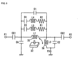
- Fig. 9 shows an equivalent circuit of a two-port isolator corresponding to a nonreciprocal circuit device according to a second embodiment of the present invention.
- the two-port isolator basically has the configuration shown as the equivalent circuit of Fig. 1 and the configurations shown in Figs. 3 to 6 , and additionally includes a resistor R2 and a series resonance circuit (including an inductor L4 and a capacitor C4) which are arranged in parallel to the first central electrode 35.
- Figs. 10(A) and 10(B) show pieces of measurement data as characteristics of the two-port isolator which corresponds to the equivalent circuit shown in Fig. 9 , which has the configurations shown in Figs. 3 to 6 , and which has the following specifications.
- Fig. 10(A) shows isolation characteristics.
- a curve A denoted by a dot line corresponds to data of the second embodiment.
- a curve A' denoted by a solid line corresponds to data of a comparative example which has specifications the same as those of the second embodiment and which does not include the series resonance circuits (including the inductors L3 and L4 and the capacitors C3 and C4).
- An isolation bandwidth is considerably increased.
- Fig. 10(B) shows insertion loss characteristics.
- a curve B denoted by a dot line corresponds to data of the second embodiment.
- a curve B' denoted by a solid line corresponds to data of the comparative example.
- the second embodiment has an insertion loss characteristic similar to that of the comparative example.
- nonreciprocal circuit device is not limited to the forgoing embodiments, and various modification may be made within a scope of the invention.
- the input port P1 and the output port P2 are also inverted.
- various modifications of shapes of the first central electrode 35 and the second central electrode 36 may be made.
- the first central electrode 35 is divided into two on the first main surface 32a and second main surface 32b of the ferrite 32 according to the first embodiment, the first central electrode 35 may not be divided into two.
- the second central electrode 36 should be wound by at least one turn.
- the present invention is effectively used for the nonreciprocal circuit device.
- the present invention is excellent in terms of capability of improving an isolation characteristic without increasing insertion loss.
Landscapes
- Non-Reversible Transmitting Devices (AREA)
- Glass Compositions (AREA)
- Networks Using Active Elements (AREA)
- Hall/Mr Elements (AREA)
- Coils Or Transformers For Communication (AREA)
Applications Claiming Priority (2)
| Application Number | Priority Date | Filing Date | Title |
|---|---|---|---|
| JP2007226641 | 2007-08-31 | ||
| PCT/JP2007/071213 WO2009028112A1 (ja) | 2007-08-31 | 2007-10-31 | 非可逆回路素子 |
Publications (3)
| Publication Number | Publication Date |
|---|---|
| EP2184802A1 true EP2184802A1 (de) | 2010-05-12 |
| EP2184802A4 EP2184802A4 (de) | 2010-12-15 |
| EP2184802B1 EP2184802B1 (de) | 2011-11-23 |
Family
ID=40386856
Family Applications (1)
| Application Number | Title | Priority Date | Filing Date |
|---|---|---|---|
| EP07830947A Not-in-force EP2184802B1 (de) | 2007-08-31 | 2007-10-31 | Nicht-reziproke schaltvorrichtung |
Country Status (5)
| Country | Link |
|---|---|
| US (1) | US7532084B2 (de) |
| EP (1) | EP2184802B1 (de) |
| CN (1) | CN101473490B (de) |
| AT (1) | ATE535039T1 (de) |
| WO (1) | WO2009028112A1 (de) |
Families Citing this family (15)
| Publication number | Priority date | Publication date | Assignee | Title |
|---|---|---|---|---|
| EP2109179A4 (de) * | 2007-02-07 | 2010-10-27 | Murata Manufacturing Co | Nichtreversibles schaltungselement |
| JP4596032B2 (ja) * | 2008-04-09 | 2010-12-08 | 株式会社村田製作所 | フェライト・磁石素子の製造方法、非可逆回路素子の製造方法及び複合電子部品の製造方法 |
| JP5126248B2 (ja) * | 2010-02-25 | 2013-01-23 | 株式会社村田製作所 | 非可逆回路素子 |
| JP5158146B2 (ja) * | 2010-07-20 | 2013-03-06 | 株式会社村田製作所 | 非可逆回路素子 |
| CN103608968B (zh) | 2011-06-16 | 2015-08-05 | 株式会社村田制作所 | 不可逆电路元件 |
| CN104081579B (zh) * | 2012-02-06 | 2016-02-24 | 株式会社村田制作所 | 不可逆电路元件 |
| WO2014013868A1 (ja) | 2012-07-19 | 2014-01-23 | 株式会社村田製作所 | 送信モジュール |
| WO2014112460A1 (ja) * | 2013-01-18 | 2014-07-24 | 株式会社村田製作所 | 非可逆回路素子 |
| JP5983859B2 (ja) * | 2013-03-08 | 2016-09-06 | 株式会社村田製作所 | 非可逆回路素子及びモジュール |
| CN105934850B (zh) * | 2014-01-27 | 2018-11-16 | 株式会社村田制作所 | 不可逆电路元件 |
| US9906199B2 (en) | 2015-03-16 | 2018-02-27 | Tdk Corporation | Magnetoresistive effect device |
| CN107431261A (zh) * | 2015-03-27 | 2017-12-01 | 株式会社村田制作所 | 不可逆电路元件、高频电路及通信装置 |
| US9966922B2 (en) * | 2016-05-25 | 2018-05-08 | Tdk Corporation | Magnetoresistive effect device |
| CN107565919B (zh) * | 2017-08-21 | 2020-11-17 | 南京理工大学 | 一种一体化封装结构的s波段隔离放大器 |
| JP7297489B2 (ja) * | 2019-03-26 | 2023-06-26 | キヤノン株式会社 | 振動型アクチュエータおよび振動型アクチュエータの駆動装置 |
Family Cites Families (11)
| Publication number | Priority date | Publication date | Assignee | Title |
|---|---|---|---|---|
| US4210886A (en) * | 1978-09-18 | 1980-07-01 | Motorola, Inc. | Isolator having reactive neutralizing means and predetermined angle between input-output windings |
| JP4655257B2 (ja) | 2001-08-01 | 2011-03-23 | 日立金属株式会社 | 2端子対アイソレータ |
| EP1246292A3 (de) | 2001-03-30 | 2003-12-10 | Hitachi Metals, Ltd. | Zweiweg-Isolator und Verfahren zu seiner Beurteilung |
| US6965276B2 (en) * | 2002-07-04 | 2005-11-15 | Murata Manufacturing Co., Ltd. | Two port type isolator and communication device |
| JP3858853B2 (ja) | 2003-06-24 | 2006-12-20 | 株式会社村田製作所 | 2ポート型アイソレータ及び通信装置 |
| CN100492758C (zh) * | 2004-07-30 | 2009-05-27 | 株式会社村田制作所 | 双端口隔离器及通信装置 |
| CN100492757C (zh) * | 2005-01-28 | 2009-05-27 | 株式会社村田制作所 | 双端口不可逆电路器件及通信装置 |
| JP2007046229A (ja) | 2005-08-05 | 2007-02-22 | Hitoshi Nagaiwa | ダヴテイル拡開アンカー設置方法とダヴテイル拡開アンカー |
| US7420435B2 (en) | 2005-10-21 | 2008-09-02 | Murata Manufacturing Co., Ltd. | Non-reciprocal circuit element, method for manufacturing the same, and communication device |
| US7737801B2 (en) | 2005-12-16 | 2010-06-15 | Hitachi Metals, Ltd. | Non-reciprocal circuit device |
| JP4356787B2 (ja) * | 2006-01-30 | 2009-11-04 | 株式会社村田製作所 | 非可逆回路素子及び通信装置 |
-
2007
- 2007-10-04 US US11/867,214 patent/US7532084B2/en active Active
- 2007-10-31 EP EP07830947A patent/EP2184802B1/de not_active Not-in-force
- 2007-10-31 AT AT07830947T patent/ATE535039T1/de active
- 2007-10-31 CN CN2007800015950A patent/CN101473490B/zh not_active Expired - Fee Related
- 2007-10-31 WO PCT/JP2007/071213 patent/WO2009028112A1/ja not_active Ceased
Also Published As
| Publication number | Publication date |
|---|---|
| EP2184802B1 (de) | 2011-11-23 |
| US20090058551A1 (en) | 2009-03-05 |
| CN101473490A (zh) | 2009-07-01 |
| ATE535039T1 (de) | 2011-12-15 |
| EP2184802A4 (de) | 2010-12-15 |
| US7532084B2 (en) | 2009-05-12 |
| CN101473490B (zh) | 2012-09-05 |
| WO2009028112A1 (ja) | 2009-03-05 |
Similar Documents
| Publication | Publication Date | Title |
|---|---|---|
| EP2184802B1 (de) | Nicht-reziproke schaltvorrichtung | |
| EP1939973B1 (de) | Irreversibles schaltelement, herstellungsverfahren dafür und kommunikationsvorrichtung | |
| EP2383835A2 (de) | Nichtreziprokes Schaltungselement | |
| WO2009154024A1 (ja) | 非可逆回路素子 | |
| JP4155342B1 (ja) | 非可逆回路素子 | |
| JP4793350B2 (ja) | 2ポート型非可逆回路素子 | |
| EP1970991B1 (de) | Nichtreziproke schaltungsanordnung | |
| EP2109179A1 (de) | Nichtreversibles schaltungselement | |
| JP4665786B2 (ja) | 非可逆回路素子及び通信装置 | |
| JP2009302742A (ja) | 非可逆回路素子 | |
| CN101779328B (zh) | 不可逆电路元件 | |
| JP4831234B2 (ja) | 非可逆回路素子 | |
| JP4760981B2 (ja) | 非可逆回路素子 | |
| JP4915366B2 (ja) | 非可逆回路素子 | |
| JP5083113B2 (ja) | 非可逆回路素子 | |
| JP4929488B2 (ja) | 非可逆回路素子 | |
| JP2007306148A (ja) | 非可逆回路素子及び通信装置 | |
| JP2012138719A (ja) | 非可逆回路素子及びフェライト・磁石素子 | |
| JP2010147853A (ja) | 非可逆回路素子 | |
| JP2012090141A (ja) | 非可逆回路素子 | |
| JP2013162197A (ja) | 非可逆回路素子 | |
| JP2012090140A (ja) | 非可逆回路素子 |
Legal Events
| Date | Code | Title | Description |
|---|---|---|---|
| PUAI | Public reference made under article 153(3) epc to a published international application that has entered the european phase |
Free format text: ORIGINAL CODE: 0009012 |
|
| 17P | Request for examination filed |
Effective date: 20080521 |
|
| AK | Designated contracting states |
Kind code of ref document: A1 Designated state(s): AT BE BG CH CY CZ DE DK EE ES FI FR GB GR HU IE IS IT LI LT LU LV MC MT NL PL PT RO SE SI SK TR |
|
| AX | Request for extension of the european patent |
Extension state: AL BA HR MK RS |
|
| DAX | Request for extension of the european patent (deleted) | ||
| A4 | Supplementary search report drawn up and despatched |
Effective date: 20101111 |
|
| RIC1 | Information provided on ipc code assigned before grant |
Ipc: H01P 1/365 20060101ALN20101105BHEP Ipc: H01P 1/36 20060101AFI20101105BHEP |
|
| REG | Reference to a national code |
Ref country code: DE Ref legal event code: R079 Ref document number: 602007018966 Country of ref document: DE Free format text: PREVIOUS MAIN CLASS: H01P0001320000 Ipc: H01P0001360000 |
|
| GRAP | Despatch of communication of intention to grant a patent |
Free format text: ORIGINAL CODE: EPIDOSNIGR1 |
|
| RIC1 | Information provided on ipc code assigned before grant |
Ipc: H01P 1/365 20060101ALN20110421BHEP Ipc: H01P 1/36 20060101AFI20110421BHEP |
|
| GRAS | Grant fee paid |
Free format text: ORIGINAL CODE: EPIDOSNIGR3 |
|
| GRAA | (expected) grant |
Free format text: ORIGINAL CODE: 0009210 |
|
| AK | Designated contracting states |
Kind code of ref document: B1 Designated state(s): AT BE BG CH CY CZ DE DK EE ES FI FR GB GR HU IE IS IT LI LT LU LV MC MT NL PL PT RO SE SI SK TR |
|
| REG | Reference to a national code |
Ref country code: GB Ref legal event code: FG4D |
|
| REG | Reference to a national code |
Ref country code: CH Ref legal event code: EP |
|
| REG | Reference to a national code |
Ref country code: IE Ref legal event code: FG4D |
|
| REG | Reference to a national code |
Ref country code: NL Ref legal event code: VDEP Effective date: 20111123 |
|
| REG | Reference to a national code |
Ref country code: DE Ref legal event code: R096 Ref document number: 602007018966 Country of ref document: DE Effective date: 20120308 |
|
| LTIE | Lt: invalidation of european patent or patent extension |
Effective date: 20111123 |
|
| PG25 | Lapsed in a contracting state [announced via postgrant information from national office to epo] |
Ref country code: IS Free format text: LAPSE BECAUSE OF FAILURE TO SUBMIT A TRANSLATION OF THE DESCRIPTION OR TO PAY THE FEE WITHIN THE PRESCRIBED TIME-LIMIT Effective date: 20120323 Ref country code: LT Free format text: LAPSE BECAUSE OF FAILURE TO SUBMIT A TRANSLATION OF THE DESCRIPTION OR TO PAY THE FEE WITHIN THE PRESCRIBED TIME-LIMIT Effective date: 20111123 |
|
| PG25 | Lapsed in a contracting state [announced via postgrant information from national office to epo] |
Ref country code: SI Free format text: LAPSE BECAUSE OF FAILURE TO SUBMIT A TRANSLATION OF THE DESCRIPTION OR TO PAY THE FEE WITHIN THE PRESCRIBED TIME-LIMIT Effective date: 20111123 Ref country code: BE Free format text: LAPSE BECAUSE OF FAILURE TO SUBMIT A TRANSLATION OF THE DESCRIPTION OR TO PAY THE FEE WITHIN THE PRESCRIBED TIME-LIMIT Effective date: 20111123 Ref country code: SE Free format text: LAPSE BECAUSE OF FAILURE TO SUBMIT A TRANSLATION OF THE DESCRIPTION OR TO PAY THE FEE WITHIN THE PRESCRIBED TIME-LIMIT Effective date: 20111123 Ref country code: GR Free format text: LAPSE BECAUSE OF FAILURE TO SUBMIT A TRANSLATION OF THE DESCRIPTION OR TO PAY THE FEE WITHIN THE PRESCRIBED TIME-LIMIT Effective date: 20120224 Ref country code: NL Free format text: LAPSE BECAUSE OF FAILURE TO SUBMIT A TRANSLATION OF THE DESCRIPTION OR TO PAY THE FEE WITHIN THE PRESCRIBED TIME-LIMIT Effective date: 20111123 Ref country code: PT Free format text: LAPSE BECAUSE OF FAILURE TO SUBMIT A TRANSLATION OF THE DESCRIPTION OR TO PAY THE FEE WITHIN THE PRESCRIBED TIME-LIMIT Effective date: 20120323 Ref country code: LV Free format text: LAPSE BECAUSE OF FAILURE TO SUBMIT A TRANSLATION OF THE DESCRIPTION OR TO PAY THE FEE WITHIN THE PRESCRIBED TIME-LIMIT Effective date: 20111123 |
|
| PG25 | Lapsed in a contracting state [announced via postgrant information from national office to epo] |
Ref country code: CY Free format text: LAPSE BECAUSE OF FAILURE TO SUBMIT A TRANSLATION OF THE DESCRIPTION OR TO PAY THE FEE WITHIN THE PRESCRIBED TIME-LIMIT Effective date: 20111123 |
|
| PG25 | Lapsed in a contracting state [announced via postgrant information from national office to epo] |
Ref country code: DK Free format text: LAPSE BECAUSE OF FAILURE TO SUBMIT A TRANSLATION OF THE DESCRIPTION OR TO PAY THE FEE WITHIN THE PRESCRIBED TIME-LIMIT Effective date: 20111123 Ref country code: BG Free format text: LAPSE BECAUSE OF FAILURE TO SUBMIT A TRANSLATION OF THE DESCRIPTION OR TO PAY THE FEE WITHIN THE PRESCRIBED TIME-LIMIT Effective date: 20120223 Ref country code: CZ Free format text: LAPSE BECAUSE OF FAILURE TO SUBMIT A TRANSLATION OF THE DESCRIPTION OR TO PAY THE FEE WITHIN THE PRESCRIBED TIME-LIMIT Effective date: 20111123 Ref country code: SK Free format text: LAPSE BECAUSE OF FAILURE TO SUBMIT A TRANSLATION OF THE DESCRIPTION OR TO PAY THE FEE WITHIN THE PRESCRIBED TIME-LIMIT Effective date: 20111123 Ref country code: EE Free format text: LAPSE BECAUSE OF FAILURE TO SUBMIT A TRANSLATION OF THE DESCRIPTION OR TO PAY THE FEE WITHIN THE PRESCRIBED TIME-LIMIT Effective date: 20111123 |
|
| PG25 | Lapsed in a contracting state [announced via postgrant information from national office to epo] |
Ref country code: RO Free format text: LAPSE BECAUSE OF FAILURE TO SUBMIT A TRANSLATION OF THE DESCRIPTION OR TO PAY THE FEE WITHIN THE PRESCRIBED TIME-LIMIT Effective date: 20111123 Ref country code: PL Free format text: LAPSE BECAUSE OF FAILURE TO SUBMIT A TRANSLATION OF THE DESCRIPTION OR TO PAY THE FEE WITHIN THE PRESCRIBED TIME-LIMIT Effective date: 20111123 Ref country code: IT Free format text: LAPSE BECAUSE OF FAILURE TO SUBMIT A TRANSLATION OF THE DESCRIPTION OR TO PAY THE FEE WITHIN THE PRESCRIBED TIME-LIMIT Effective date: 20111123 |
|
| REG | Reference to a national code |
Ref country code: AT Ref legal event code: MK05 Ref document number: 535039 Country of ref document: AT Kind code of ref document: T Effective date: 20111123 |
|
| PLBE | No opposition filed within time limit |
Free format text: ORIGINAL CODE: 0009261 |
|
| STAA | Information on the status of an ep patent application or granted ep patent |
Free format text: STATUS: NO OPPOSITION FILED WITHIN TIME LIMIT |
|
| 26N | No opposition filed |
Effective date: 20120824 |
|
| REG | Reference to a national code |
Ref country code: DE Ref legal event code: R097 Ref document number: 602007018966 Country of ref document: DE Effective date: 20120824 |
|
| PG25 | Lapsed in a contracting state [announced via postgrant information from national office to epo] |
Ref country code: AT Free format text: LAPSE BECAUSE OF FAILURE TO SUBMIT A TRANSLATION OF THE DESCRIPTION OR TO PAY THE FEE WITHIN THE PRESCRIBED TIME-LIMIT Effective date: 20111123 |
|
| PG25 | Lapsed in a contracting state [announced via postgrant information from national office to epo] |
Ref country code: ES Free format text: LAPSE BECAUSE OF FAILURE TO SUBMIT A TRANSLATION OF THE DESCRIPTION OR TO PAY THE FEE WITHIN THE PRESCRIBED TIME-LIMIT Effective date: 20120305 |
|
| PG25 | Lapsed in a contracting state [announced via postgrant information from national office to epo] |
Ref country code: MC Free format text: LAPSE BECAUSE OF NON-PAYMENT OF DUE FEES Effective date: 20121031 |
|
| REG | Reference to a national code |
Ref country code: CH Ref legal event code: PL |
|
| PG25 | Lapsed in a contracting state [announced via postgrant information from national office to epo] |
Ref country code: FI Free format text: LAPSE BECAUSE OF FAILURE TO SUBMIT A TRANSLATION OF THE DESCRIPTION OR TO PAY THE FEE WITHIN THE PRESCRIBED TIME-LIMIT Effective date: 20111123 |
|
| PG25 | Lapsed in a contracting state [announced via postgrant information from national office to epo] |
Ref country code: CH Free format text: LAPSE BECAUSE OF NON-PAYMENT OF DUE FEES Effective date: 20121031 Ref country code: LI Free format text: LAPSE BECAUSE OF NON-PAYMENT OF DUE FEES Effective date: 20121031 |
|
| REG | Reference to a national code |
Ref country code: IE Ref legal event code: MM4A |
|
| PG25 | Lapsed in a contracting state [announced via postgrant information from national office to epo] |
Ref country code: IE Free format text: LAPSE BECAUSE OF NON-PAYMENT OF DUE FEES Effective date: 20121031 |
|
| PG25 | Lapsed in a contracting state [announced via postgrant information from national office to epo] |
Ref country code: MT Free format text: LAPSE BECAUSE OF FAILURE TO SUBMIT A TRANSLATION OF THE DESCRIPTION OR TO PAY THE FEE WITHIN THE PRESCRIBED TIME-LIMIT Effective date: 20111123 |
|
| PG25 | Lapsed in a contracting state [announced via postgrant information from national office to epo] |
Ref country code: TR Free format text: LAPSE BECAUSE OF FAILURE TO SUBMIT A TRANSLATION OF THE DESCRIPTION OR TO PAY THE FEE WITHIN THE PRESCRIBED TIME-LIMIT Effective date: 20111123 |
|
| PG25 | Lapsed in a contracting state [announced via postgrant information from national office to epo] |
Ref country code: LU Free format text: LAPSE BECAUSE OF NON-PAYMENT OF DUE FEES Effective date: 20121031 |
|
| PG25 | Lapsed in a contracting state [announced via postgrant information from national office to epo] |
Ref country code: HU Free format text: LAPSE BECAUSE OF FAILURE TO SUBMIT A TRANSLATION OF THE DESCRIPTION OR TO PAY THE FEE WITHIN THE PRESCRIBED TIME-LIMIT Effective date: 20071031 |
|
| REG | Reference to a national code |
Ref country code: FR Ref legal event code: PLFP Year of fee payment: 9 |
|
| REG | Reference to a national code |
Ref country code: FR Ref legal event code: PLFP Year of fee payment: 10 |
|
| REG | Reference to a national code |
Ref country code: FR Ref legal event code: PLFP Year of fee payment: 11 |
|
| REG | Reference to a national code |
Ref country code: FR Ref legal event code: PLFP Year of fee payment: 12 |
|
| PGFP | Annual fee paid to national office [announced via postgrant information from national office to epo] |
Ref country code: FR Payment date: 20221028 Year of fee payment: 16 |
|
| PGFP | Annual fee paid to national office [announced via postgrant information from national office to epo] |
Ref country code: GB Payment date: 20221019 Year of fee payment: 16 Ref country code: DE Payment date: 20221019 Year of fee payment: 16 |
|
| REG | Reference to a national code |
Ref country code: DE Ref legal event code: R119 Ref document number: 602007018966 Country of ref document: DE |
|
| GBPC | Gb: european patent ceased through non-payment of renewal fee |
Effective date: 20231031 |
|
| PG25 | Lapsed in a contracting state [announced via postgrant information from national office to epo] |
Ref country code: GB Free format text: LAPSE BECAUSE OF NON-PAYMENT OF DUE FEES Effective date: 20231031 |
|
| PG25 | Lapsed in a contracting state [announced via postgrant information from national office to epo] |
Ref country code: GB Free format text: LAPSE BECAUSE OF NON-PAYMENT OF DUE FEES Effective date: 20231031 Ref country code: FR Free format text: LAPSE BECAUSE OF NON-PAYMENT OF DUE FEES Effective date: 20231031 Ref country code: DE Free format text: LAPSE BECAUSE OF NON-PAYMENT OF DUE FEES Effective date: 20240501 |