EP2184843B1 - Dispositif de conversion de courant alternatif de type direct - Google Patents
Dispositif de conversion de courant alternatif de type direct Download PDFInfo
- Publication number
- EP2184843B1 EP2184843B1 EP08792650.7A EP08792650A EP2184843B1 EP 2184843 B1 EP2184843 B1 EP 2184843B1 EP 08792650 A EP08792650 A EP 08792650A EP 2184843 B1 EP2184843 B1 EP 2184843B1
- Authority
- EP
- European Patent Office
- Prior art keywords
- power supply
- voltage
- capacitor
- supply line
- current
- Prior art date
- Legal status (The legal status is an assumption and is not a legal conclusion. Google has not performed a legal analysis and makes no representation as to the accuracy of the status listed.)
- Active
Links
Images


Classifications
-
- H—ELECTRICITY
- H02—GENERATION; CONVERSION OR DISTRIBUTION OF ELECTRIC POWER
- H02M—APPARATUS FOR CONVERSION BETWEEN AC AND AC, BETWEEN AC AND DC, OR BETWEEN DC AND DC, AND FOR USE WITH MAINS OR SIMILAR POWER SUPPLY SYSTEMS; CONVERSION OF DC OR AC INPUT POWER INTO SURGE OUTPUT POWER; CONTROL OR REGULATION THEREOF
- H02M1/00—Details of apparatus for conversion
- H02M1/36—Means for starting or stopping converters
-
- H—ELECTRICITY
- H02—GENERATION; CONVERSION OR DISTRIBUTION OF ELECTRIC POWER
- H02M—APPARATUS FOR CONVERSION BETWEEN AC AND AC, BETWEEN AC AND DC, OR BETWEEN DC AND DC, AND FOR USE WITH MAINS OR SIMILAR POWER SUPPLY SYSTEMS; CONVERSION OF DC OR AC INPUT POWER INTO SURGE OUTPUT POWER; CONTROL OR REGULATION THEREOF
- H02M5/00—Conversion of AC power input into AC power output, e.g. for change of voltage, for change of frequency, for change of number of phases
- H02M5/40—Conversion of AC power input into AC power output, e.g. for change of voltage, for change of frequency, for change of number of phases with intermediate conversion into DC
- H02M5/42—Conversion of AC power input into AC power output, e.g. for change of voltage, for change of frequency, for change of number of phases with intermediate conversion into DC by static converters
- H02M5/44—Conversion of AC power input into AC power output, e.g. for change of voltage, for change of frequency, for change of number of phases with intermediate conversion into DC by static converters using discharge tubes or semiconductor devices to convert the intermediate DC into AC
- H02M5/453—Conversion of AC power input into AC power output, e.g. for change of voltage, for change of frequency, for change of number of phases with intermediate conversion into DC by static converters using discharge tubes or semiconductor devices to convert the intermediate DC into AC using devices of a triode or transistor type requiring continuous application of a control signal
- H02M5/458—Conversion of AC power input into AC power output, e.g. for change of voltage, for change of frequency, for change of number of phases with intermediate conversion into DC by static converters using discharge tubes or semiconductor devices to convert the intermediate DC into AC using devices of a triode or transistor type requiring continuous application of a control signal using semiconductor devices only
- H02M5/4585—Conversion of AC power input into AC power output, e.g. for change of voltage, for change of frequency, for change of number of phases with intermediate conversion into DC by static converters using discharge tubes or semiconductor devices to convert the intermediate DC into AC using devices of a triode or transistor type requiring continuous application of a control signal using semiconductor devices only having a rectifier with controlled elements
-
- H—ELECTRICITY
- H02—GENERATION; CONVERSION OR DISTRIBUTION OF ELECTRIC POWER
- H02P—CONTROL OR REGULATION OF ELECTRIC MOTORS, ELECTRIC GENERATORS OR DYNAMO-ELECTRIC CONVERTERS; CONTROLLING TRANSFORMERS, REACTORS OR CHOKE COILS
- H02P27/00—Arrangements or methods for the control of AC motors characterised by the kind of supply voltage
- H02P27/04—Arrangements or methods for the control of AC motors characterised by the kind of supply voltage using variable-frequency supply voltage, e.g. inverter or converter supply voltage
- H02P27/06—Arrangements or methods for the control of AC motors characterised by the kind of supply voltage using variable-frequency supply voltage, e.g. inverter or converter supply voltage using DC to AC converters or inverters
-
- H—ELECTRICITY
- H02—GENERATION; CONVERSION OR DISTRIBUTION OF ELECTRIC POWER
- H02M—APPARATUS FOR CONVERSION BETWEEN AC AND AC, BETWEEN AC AND DC, OR BETWEEN DC AND DC, AND FOR USE WITH MAINS OR SIMILAR POWER SUPPLY SYSTEMS; CONVERSION OF DC OR AC INPUT POWER INTO SURGE OUTPUT POWER; CONTROL OR REGULATION THEREOF
- H02M7/00—Conversion of AC power input into DC power output; Conversion of DC power input into AC power output
- H02M7/02—Conversion of AC power input into DC power output without possibility of reversal
- H02M7/04—Conversion of AC power input into DC power output without possibility of reversal by static converters
- H02M7/12—Conversion of AC power input into DC power output without possibility of reversal by static converters using discharge tubes with control electrode or semiconductor devices with control electrode
- H02M7/21—Conversion of AC power input into DC power output without possibility of reversal by static converters using discharge tubes with control electrode or semiconductor devices with control electrode using devices of a triode or transistor type requiring continuous application of a control signal
- H02M7/217—Conversion of AC power input into DC power output without possibility of reversal by static converters using discharge tubes with control electrode or semiconductor devices with control electrode using devices of a triode or transistor type requiring continuous application of a control signal using semiconductor devices only
- H02M7/219—Conversion of AC power input into DC power output without possibility of reversal by static converters using discharge tubes with control electrode or semiconductor devices with control electrode using devices of a triode or transistor type requiring continuous application of a control signal using semiconductor devices only in a bridge configuration
-
- H—ELECTRICITY
- H02—GENERATION; CONVERSION OR DISTRIBUTION OF ELECTRIC POWER
- H02P—CONTROL OR REGULATION OF ELECTRIC MOTORS, ELECTRIC GENERATORS OR DYNAMO-ELECTRIC CONVERTERS; CONTROLLING TRANSFORMERS, REACTORS OR CHOKE COILS
- H02P2207/00—Indexing scheme relating to controlling arrangements characterised by the type of motor
- H02P2207/05—Synchronous machines, e.g. with permanent magnets or DC excitation
Definitions
- the present invention relates to a direct AC power converting apparatus, and more particularly, to a technology of preventing inrush current to a capacitor included in a direct AC power converting apparatus.
- Non-Patent Document 1 discloses a direct AC power converting apparatus including a clamp circuit.
- FIG. 24 shows the direct AC power converting apparatus described in Non-Patent Document 1. Note that for the sake of description of the present invention, reference symbols in the drawing do not necessarily correspond to those of Non-Patent Document 1.
- FIG. 25 is a graph showing the relationship between voltage between both ends and electrostatic capacitance of the clamp capacitor, which is based on Expression (2).
- the power supply voltage Vs is 400 V
- the inductance La is 12 mH
- the overload current i is 40 A
- the electrostatic capacitance of the clamp capacitor is 10 ⁇ F
- the voltage Vc between both ends of the clamp capacitor is approximately 1,800 V.
- the power supply value exceeds device rating 1,200 V of a transistor and a diode with power supply voltage of 400 V class.
- the electrostatic capacitance of the clamp capacitor needs to be 200 ⁇ F or larger from Expression (2) and FIG. 25 .
- FIG. 26 is a graph showing the relationship between inrush current (i(([pi]-[alpha])/[omega])) and the electrostatic capacitance C.
- the voltage between both ends of the clamp capacitor charged with the regenerative current is approximately equal to or lower than 750 V, and accordingly if the electrostatic capacitance of the clamp capacitor is 200 [micro]F, the maximum value (inrush current) of current reaches 150 A from Expressions (6) and (7).
- Patent Documents 1 to 4 disclose the technologies related to the present invention.
- a power control system includes a three-phase rectifier for rectifying a three-phase AC voltage into a DC voltage, a first contactor for providing or breaking the three-phase AC voltage to the three-phase rectifier, a charging unit for charging the DC voltage rectifier through the three-phase rectifier, and a bypass circuit for bypassing the first contactor and providing the three-phase AC voltage to the charging circuit, the bypass circuit comprising: a current limiter placed in the bypass circuit for limiting bypassed current which flows into the charging circuit, and a second connector placed in the bypass circuit for providing or breaking a bypassed DC voltage to the charging circuit.
- An object of the present invention is therefore to provide a direct AC power converting apparatus capable of reducing inrush current while increasing electrostatic capacitance of a capacitor to prevent an increase in voltage between both ends of the capacitor.
- a direct AC power converting apparatus includes the features of claim 1.
- the direct AC power converting apparatus further includes a second diode (D5) connected, between the positive-side DC power supply line (L1) and the negative-side DC power supply line (L2), in series with the first diode (D1), and having an anode on the positive-side DC power supply line (L1) side and a cathode on the negative-side DC power supply line (L2) side, wherein the neutral phase input line (ACLn) is connected between the first and second diodes.
- a second diode (D5) connected, between the positive-side DC power supply line (L1) and the negative-side DC power supply line (L2), in series with the first diode (D1), and having an anode on the positive-side DC power supply line (L1) side and a cathode on the negative-side DC power supply line (L2) side, wherein the neutral phase input line (ACLn) is connected between the first and second diodes.
- the direct AC power converting apparatus further includes a switch (S1) provided on the neutral phase input line (ACLn), wherein the control section (5) supplies for charging of the first capacitor (Cc1) and the second capacitor (Cc2) in a state in which the switch is in conduction, and brings the switch into nonconduction after a lapse of a predetermined period of time.
- a switch S1 provided on the neutral phase input line (ACLn)
- the control section (5) supplies for charging of the first capacitor (Cc1) and the second capacitor (Cc2) in a state in which the switch is in conduction, and brings the switch into nonconduction after a lapse of a predetermined period of time.
- the resistor (R1) is provided on the neutral phase input line (ACLn).
- the resistor (R1) is provided in one of the plurality of input lines (ACLr, ACLs, ACLt), the direct AC power converting apparatus further including reactors (Lr, Ls, Lt) connected in parallel with the resistor.
- the AC voltage for one phase is subjected to voltage doubler rectification to charge the first capacitor and the second capacitor, whereby it is possible to prevent the inrush current from flowing from the multi-phase AC power supply to the first capacitor and the second capacitor in an initial operation of the current-source power converter. Since the resistor is provided in a path of the charging, the inrush current does not flow in the charging as well. On this occasion, the input capacitor is not electrically connected to the first capacitor and the second capacitor. Therefore, the inrush current does not flow from the input capacitor to the first capacitor and the second capacitor even if the input capacitor is charged with voltage.
- the first capacitor and the second capacitor are charged in the state of being connected in series with each other by the rectifying functions of the first, third and fourth diodes, and discharged in the state of being connected in parallel with each other.
- the first capacitor and the second capacitor are charged with a regenerative current from an inductive multi-phase load, and discharged when exceeding a voltage value which is determined based on the load power factor on the voltage-source power converting apparatus side. That is, it is possible to secure a discharging path by the first capacitor and the second capacitor, and accordingly there can be achieved an operation similar to an operation of a system described in Non-Patent Document 1, though it is a passive circuit.
- the direct AC power converting apparatus of the sixth aspect which is according to the direct AC power converting apparatus of the third aspect according to the second aspect, in the normal operation in which the current-source power converter converts a multi-phase AC voltage into a DC voltage having two potentials, and the voltage-source power converter converts the DC voltage into a square-wave-shape AC voltage, the switch is in nonconduction. Accordingly, a voltage between the input lines is applied to a pair of the first capacitor and the second capacitor.
- the voltage serving as a reference for discharging the first capacitor and the second capacitor in the state of being connected in parallel with each other comes a half value, while it is 1/ ⁇ 3 of the maximum value of the voltage between the inout lines in the case where the switch is in the conductive state. Accordingly, the waveform of the input current can be improved.
- the current-source power converter converts a multi-phase AC voltage into a DC voltage having two potentials and the voltage-source power converter converts the DC voltage into a square-wave-shape AC voltage, it is possible to prevent the second capacitor from being charged/discharged through the neutral phase input line, which accordingly prevents a loss of symmetry of the input currents.
- the third aspect of the direct AC power converting apparatus of the present invention in the normal operation in which the current-source power converter converts a multi-phase AC voltage into a DC voltage having two potentials and the voltage-source power converter converts the DC voltage into a square-wave-shape AC voltage, connection of the power supply to the first capacitor and the second capacitor through the neutral phase input line is cut off. Accordingly, it is possible to prevent the second capacitor from being charged/discharged through the neutral phase input line, which accordingly prevents a loss of symmetry of the input currents.
- the current-source power converter converts the multi-phase AC voltage applied between ones of the input lines into the DC voltage to supply to the first capacitor and the second capacitor, whereby the input capacitor is connected in parallel with the first capacitor and the second capacitor.
- the first capacitor and the second capacitor have been applied with the voltage subjected to voltage doubler rectification until then, and thus a voltage between both ends of a pair of the first capacitor and the second capacitor is larger than a voltage between both ends of the input capacitor. Accordingly, in a case where the input capacitor is connected in parallel with the first capacitor and the second capacitor, it is possible to effectively prevent the inrush current from flowing from the input capacitor to the first capacitor and the second capacitor.
- the resistor is provided in the neutral phase input line, whereby it is possible to supply the DC current to the first capacitor and the second capacitor through the resistor by using any of the input lines.
- the direct AC power converting apparatus of the present invention it is possible to compose a carrier current component removing filter for removing a carrier current component by the reactor and the input capacitor.
- the resistor and the reactor are connected in parallel with each other, whereby it is possible to reduce pulsation of a voltage of the input capacitor in an initial charging period (transient period).
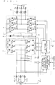
- FIG. 1 shows a conceptual configuration of a motor driving device as an example of a direct AC power converting apparatus according to a first comparative example useful for understanding the invention.
- the motor driving device includes a power supply El, input lines ACLr, ACLs and ACLt, a neutral phase input line ACLn, reactors Lr, Ls and Lt, capacitors Cr, Cs and Ct, a current-source converter 1, DC power supply lines L1 and L2, a clamp circuit 2, a voltage-source inverter 3, a motor 4, a control section 5, a resistor R1 and a switch S1.
- the power supply E1 is a multi-phase AC power supply including a neutral point (not shown), which is, for example, a three-phase AC power supply.
- the input lines ACLr, ACLs and ACLt are supplied with an output of the power supply E1.
- the reactors Lr, Ls and Lt are provided on the input lines ACLr, ACLs and ACLt, respectively.
- Each of the capacitors Cr, Cs and Ct is connected between ones of the input lines ACLr, ACLs and ACLt through, for example, Y-connection. More specifically, the capacitors Cr and Cs are connected in series between the input lines ACLr and ACLs, the capacitors Cs and Ct are connected in series between the input lines ACLs and ACLt, and the capacitors Ct and Cr are connected in series between the input lines ACLt and ACLr. Those are provided on an input side of the current-source converter 1 and function as a voltage source.
- the capacitors Cr, Cs and Ct are considered to be input capacitors.
- the capacitors Cr, Cs and Ct are also considered to constitute, together with the reactors Lr, Ls and Lt, a carrier current component removing filter for removing a carrier current component, respectively.
- the current-source converter 1 includes a plurality of switch devices, and converts a three-phase AC voltage applied to ones of the input lines ACLr, ACLs and ACLt into a square-wave-shape DC voltage having two potentials by selection operations of the plurality of switch devices, to thereby supply the DC voltage between the DC power supply lines L1 and L2.
- the DC power supply line L1 is considered to be a positive-side DC power supply line
- the DC power supply line L2 is considered to be a negative-side DC power supply line to which a potential lower than that of the DC power supply line L1 is applied.
- the current-source converter 1 includes transistors Srp, Srn, Ssp, Ssn, Stp and Stn, and diodes Drp, Drn, Dsp, Dsn, Dtp and Dtn.
- Respective cathodes of the diodes Drp, Dsp and Dtp are connected to the DC power supply line L1.
- Respective anodes of the diodes Drn, Dsn and Dtn are connected to the DC power supply line L2.
- Emitters of the transistors Srp, Ssp and Stp are connected to anodes of the diodes Drp, Dsp and Dtp, respectively.
- Collectors of the transistors Srn, Ssn and Stn are connected to cathodes of the diodes Drn, Dsn and Dtn, respectively.
- a collector of the transistor Srp and an emitter of the transistor Srn, a collector of the transistor Ssp and an emitter of the transistor Ssn, and a collector of the transistor Stp and an emitter of the transistor Stn are connected in common to the input lines ACLr, ACLs and ACLt, respectively.
- Respective bases of those transistors Srp, Srn, Ssp, Ssn, Stp and Stn are supplied with a switch signal by the control section 5, and the current-source converter 1 converts the three-phase AC voltage into a square-wave-shape DC voltage having two potentials.
- the clamp circuit 2 includes clamp capacitors Cc1 and Cc2 and a diode D1.
- the diode D1 is connected between the DC power supply lines L1 and L2, with an anode and a cathode thereof connected to the DC power supply line L1 side and the DC power supply line L2 side, respectively.
- the clamp capacitors Cc1 and Cc2 are both connected in series with the diode D1.
- the clamp capacitors Cc1 and Cc2 and the diode D1 are connected in series with each other.
- the neutral phase input line ACLn connects the neutral point of the power supply E1 and a point between the clamp capacitors Cc1 and Cc2.
- the resistor R1 is inserted in the neutral phase input line ACLn.
- the switch S1 is provided in series with the resistor R1 on the neutral phase input line ACLn.
- the voltage-source inverter 3 converts the square-wave-shape DC voltage between the DC power supply lines L1 and L2 into a square-wave-shape AC voltage and outputs the AC voltage to the motor 4. More specifically, the voltage-source inverter 3 includes transistors Sup, Sun, Svp, Svn, Swp and Swn, and diodes Dup, Dun, Dvp, Dvn, Dwp and Dwn.
- Respective collectors of the transistors Sup, Svp and Swp and respective cathodes of the diodes Dup, Dvp and Dwp are connected to the DC power supply line L1
- respective emitters of the transistors Sun, Svn and Swn and respective anodes of the diodes Dun, Dvn and Dwn are connected to the DC power supply line L2.
- An emitter of the transistor Sup, a collector of the transistor Sun, an anode of the diode Dup and a cathode of the diode Dun are connected in common to the motor 4, an emitter of the transistor Svp, a collector of the transistor Svn, an anode of the diode Dvp and a cathode of the diode Dvn are connected in common to the motor 4, and an emitter of the transistor Swp, a collector of the transistor Swn, an anode of the diode Dwp and a cathode of the diode Dwn are connected in common to the motor 4.
- Bases of those transistors Sup, Sun, Svp, Svn, Swp and Swn are supplied with the switch signal by, for example, the control section 5, and the voltage-source inverter 3 converts the square-wave-shape DC voltage between the DC power supply lines L1 and L2 into a square-wave-shape AC voltage and outputs the AC voltage to the motor 4.
- the motor 4 is, for example, a three-phase AC motor, and an inductance component and a resistance component thereof are represented by coils Lu, Lv and Lw, and resistors Ru, Rv and Rw which are connected in series therewith, respectively.
- Those series connections correspond to respective phases of the motor 4.
- One ends of those series connections are connected between the transistors Sup and Sun, between the transistors Svp and Svn, and between the transistors Swp and Swn, respectively.
- the other ends of those series connections are connected in common at a neutral point N.
- the voltage-source inverter 3 supplies the square-wave-shape AC voltage. Thanks to the inductance component of the motor 4, an AC current for driving the motor 4 is smoothed. In other words, the motor 4 converts the square-wave-shape AC voltage supplied from the voltage-source inverter 3 into the AC current.
- the capacitors Cr, Cs and Ct are charged with the AC current flowing through the motor 4 via the voltage-source inverter 3 and the current-source converter 1, which is converted into the AC voltage.
- the motor 4 is also considered to be a current source for the current-source converter 1.
- the control section 5 controls selection operations of the switch S1 and transistors of the current-source converter 1.
- the control section 5 controls the selection operation of the transistors of the current-source converter 1 in a sate where the switch S1 is in conduction, and performs voltage doubler rectification on a line current for one phase, which flows through one (for example, input line ACLr) of the input lines and the neutral phase input line ACLn via the resistor R1 to supply it to the clamp capacitors Cc1 and Cc2, to thereby bring the switch S1 into nonconduction after a lapse of a given period of time.
- control section 5 includes an energization detecting and synchronization signal generating section 51 and a switching control section 52.
- the energization detecting and synchronization signal generating section 51 detects the AC currents flowing through, for example, given two phases (for example, input lines ACLr and ACLs) of the power supply E1 to generate a synchronization signal, and supplies the synchronization signal to the switching control section 52. In addition, the energization detecting and synchronization signal generating section 51 supplies a switch signal to the switch S1.
- the switching control section 52 supplies switching signals to the transistors of the current-source converter 1 in synchronization with the input synchronization signal.
- FIG. 2 is a flowchart showing the operation of the control section 5.
- Step ST1 the energization detecting and synchronization signal generating section 51 receives an activation command from, for example, an external CPU etc. Then, in Step ST2, the energization detecting and synchronization signal generating section 51 which has received the activation command detects the AC currents flowing through, for example, the given two phases (for example, input lines ACLr and ACLs) of the power supply E1, and generates a synchronization signal based on a period of the AC currents, to thereby supply the synchronization signal to the switching control section 52. Accordingly, the energization detecting and synchronization signal generating section 51 and the switching control section 52 are respectively capable of outputting switch signals in synchronization with each other.
- Step ST3 the energization detecting and synchronization signal generating section 51 sends the switch signal to the switch S1 to bring the switch S1 into conduction.
- Step ST4 in synchronization with the received synchronization signal, the switching control section 52 performs voltage doubler rectification on a phase voltage for one phase between one (for example, input line ACLr) of the input lines and the neutral phase input line ACLn for charging of the clamp capacitors Cc1 and Cc2. Specifically, the switching control section 52 starts, for example, the control of the transistors Srp and Srn.
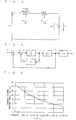
- FIG. 3 is a figure showing a voltage Vrn between the input line ACLr and the neutral phase input line ACLn, conductive/nonconductive states of the transistors Srp and Srn. Note that in FIG. 3 the voltage Vrn is positive when the voltage Vrn has high potential on the input line ACLr side.
- the switching control section 52 brings the transistor Srp into conduction in a half period in which the voltage Vrn has high potential on the input line ACLr side, and brings the transistor Srn into conduction in the other half period.
- the clamp capacitor Cc1 is charged in a state where the transistor Srp is in conduction
- the clamp capacitor Cc2 is charged in a state where the transistor Srn is in conduction.
- the resistor R1 is inserted in both charging paths of the clamp capacitors Cc1 and Cc2, whereby the DC voltage is applied to the clamp capacitors Cc1 and Cc2 through the resistor R1. Therefore, it is possible to prevent the inrush current from flowing from the power supply E1 to the clamp capacitors Cc1 and Cc2.
- FIG. 4 is a diagram showing this circuit
- FIG. 5 is a block diagram in which a current ic flowing through the capacitor C when the power supply voltage Vs is input is assumed to be an output.
- a transfer characteristic G(s) of the current ic to the power supply voltage Vs is similar to Expression (1).
- Expression (2) is derived.
- a resistance value R of the resistor R1 is large, and a transient response (within a range of small s) is taken into account, whereby the following expression is derived if the transfer characteristic is approximated with time-lag of first order.
- D 1/L
- E R/L
- F 1/LC
- FIG. 6 represents Expression (9) graphically, which shows the relationship between the current flowing through the capacitor and time.
- FIG. 6 shows the results obtained in a case where an inductance of the reactor L is 1 mH, an electrostatic capacitance of the capacitor C is 330 ⁇ F, a resistance value of the resistor R is 10 ⁇ , and the power supply voltage Vs is 400 V.
- Step ST5 the energization detecting and synchronization signal generating section 51 determines whether or not a predetermined period of time has passed from the start of Step ST4, and executes Step ST5 again if it has not passed. If it has passed, in Step ST6, the energization detecting and synchronization signal generating section 51 brings the switch S1 into nonconduction. Since the switch S1 is in nonconduction, the AC current from the power supply E1 does not flow through the resistor R1. Accordingly, it is possible to prevent the generation of loss produced in the resistor R1 after restricting the inrush current.
- Step ST4 the clamp capacitors Cc1 and Cc2 are supplied with the phase voltage for one phase between, for example, the input line ACLr and the neutral phase input line ACLn, and thus the capacitors Cr, Cs and Ct are not connected to the clamp capacitors Cc1 and Cc2. Accordingly, it is possible to prevent the inrush current from flowing from the capacitors Cr, Cs and Ct to the clamp capacitors even if the capacitors Cr, Cs and Ct are charged.
- Step ST7 the direct AC power converting apparatus is activated, to thereby shift to a normal operation. More specifically, in order to switch the switching operation of the current-source converter 1 to a normal operation, the current-source converter 1 is activated again, and the voltage-source inverter 3 is also activated. In the normal operation, the switching control section 52 supplies switch signals to the transistors Srp, Srn, Ssp, Ssn, Stp and Stn to operate the current-source converter 1, thereby converting the AC voltage input from the input lines ACLr, ACLs and ACLt into a square-wave-shape DC voltage having two potentials to supply the DC voltage to the DC power supply lines L1 and L2.
- the voltage-source inverter 3 operates, for example, in synchronization with the current-source converter 1, and converts the square-wave-shape DC voltage between the DC power supply lines L1 and L2 into a square-wave-shape AC voltage to apply the AC voltage to the motor 4.
- the clamp capacitors Cc1 and Cc2 are applied with the DC voltage subjected to voltage doubler rectification in Step ST4, and thus a voltage between both ends of a pair of the clamp capacitors Cc1 and Cc2 is higher than, for example, a voltage between both ends of a pair of the capacitors Cr and Cs (specifically, 2 / 3 times). Accordingly, it is possible to, in starting the normal operation, effectively prevent the current initially flowing from the capacitors Cr and Cs to the clamp capacitors Cc1 and Cc2 from flowing as the inrush current.
- this motor driving apparatus it is possible to prevent inrush current from flowing from the power supply E1 to the clamp capacitors Cc1 and Cc2. Moreover, it is possible to, in starting the normal operation, effectively prevent inrush current from flowing from the capacitors Cr, Cs and Ct to the clamp capacitors Cc1 and Cc2.
- a current-source converter is not typically provided with a current limiting resistor because a reactor is typically provided for output of a current-source converter.
- a current limiting resistor for preventing charging current which initially flows from flowing to those as inrush current.
- Step ST4 the switching control section 52 brings the transistor Srp into conduction in a half period in which the voltage Vrn has high potential on the input line ACLr side and brings the transistor Srn into conduction in the other half period, which is not limited thereto.
- the switching control section 52 brings the transistor Srp into conduction in a half period in which the voltage Vrn has high potential on the input line ACLr side and brings the transistor Srn into conduction in the other half period, which is not limited thereto.
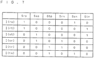
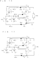
- FIGS. 7 to 9 are figures for describing the switching operation of the current-source converter 1 in the normal operation.
- the switching control section 52 outputs switch signals to the current-source converter 1 so that six switching modes are selected in succession as shown in, for example, FIG. 7 .
- " 1 " and "0" represent a state in which the transistor is in conduction and a state in which the transistor is in nonconduction, respectively
- I(P) P is any of rs, rt, st, sr, tr and ts
- I(P) P is any of rs, rt, st, sr, tr and ts
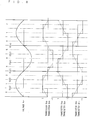
- FIG. 8 shows the voltage Vrn between the input line ACLr and the neutral phase input line ACLn, and conduction/nonconduction states of the transistors Srp, Srn, Ssp, Ssn, Stp and Stn. Note that the conduction/nonconduction in the normal operation is indicated by a broken line, and the conductive states of the transistors Srn, Ssn and Stn are represented by "-1". In addition, for example, the transistors are shifted linearly from the 0 (nonconduction) state to the 1 or -1 (conduction) state. If, for example, a pulse width of a switch signal supplied to a transistor is controlled, the switch operation as described above can be substantially achieved.
- the current vector output from the current-source converter 1 describes a locus of a hexagon with respective current vectors I(P) being as vertices by the switching operation shown in FIG. 8 , as shown in, for example, FIG. 9 .
- the switching control section 52 outputs switch signals to the transistors Srp, Ssp, Stp, Srn, Ssn and Stn, and converts a three-phase AC voltage input from the input lines ACLr, ACLs and ACLt into a square-wave-shape DC voltage having two potentials to supply the DC voltage to the DC power supply lines L1 and L2.
- Step ST4 the switching control section 52 controls the selection operations of the transistors Srp and Srn as, for example, indicated by a solid line in FIG. 8 . This is achieved by outputting switch signals to the transistors Srp and Srn so that the nearest current vector is output within a phase angle ( ⁇ t) of each mode shown in FIG. 9 . Note that the selection operation of the transistors Ssp and Ssn may be controlled.
- the resistor R1 is arranged in the case where the clamp capacitors Cc1 and Cc2 are charged using the phase voltage for one phase between the input line ACLr and the neutral phase input line ACLn, which prevents the inrush current from flowing from the power supply E1 to the clamp capacitors Cc1 and Cc2.
- the voltage doubler rectification is performed for charging the clamp capacitors Cc1 and Cc2, which also prevents the inrush current from flowing from the capacitors Cr, Cs and Ct to the clamp capacitors Cc1 and Cc2 in starting the normal operation.
- the switching operation in the normal operation is applicable, whereby there is no need to generate a waveform dedicated to charging contrary to, for example, the case shown in FIG. 3 .
- the switching operation of the current-source converter 1 in Step ST4 and the switching operation of the current-source converter 1 in the normal operation can be switched without activating the current-source converter 1 again, whereby it is not necessarily required to activate the current-source converter 1 again in Step ST7.
- FIG. 10 shows a conceptual configuration of the motor driving device as the other example of the direct AC power converting apparatus according to the first comparative example.
- the motor driving device shown in FIG. 10 is the same as the motor driving device shown in FIG. 1 except for the clamp circuit 2. Note that in FIG. 10 , circuits at the stages subsequent to the clamp circuit 2 are omitted.
- the clamp circuit 2 includes the clamp capacitors Cc1 and Cc2 and diodes D2 to D4.
- the clamp capacitor Cc1 is connected between the DC power supply lines L1 and L2.
- the clamp capacitor Cc2 is connected in series with the clamp capacitor Cc1 and is provided on the DC power supply line L2 side with respect to the clamp capacitor Cc1.
- the diode D2 is connected between the clamp capacitors Cc1 and Cc2, with its anode connected to the clamp capacitor Cc1 and its cathode connected to the clamp capacitor Cc2.
- the diode D3 has an anode connected between the clamp capacitor Cc2 and the diode D2 and a cathode connected to the DC power supply line L1.
- the diode D4 has an anode connected to the DC power supply line L2 and a cathode connected between the clamp capacitor Cc1 and the diode D2.
- the clamp capacitors Cc1 and Cc2 are discharged in a state of being connected in parallel with each other when respective voltages between both ends of the clamp capacitors Cc1 and Cc2 rise higher than a voltage which is lower one of the square-wave-shape DC voltages between the DC power supply lines L1 and L2.
- the clamp capacitors Cc1 and Cc2 are charged in the state of being connected in series with each other and discharged in the state of being connected in parallel with each other, and accordingly a discharging voltage is a half of the charging voltage.
- the voltages of the clamp capacitors Cc1 and Cc2 are balanced in a case where the discharging current is larger than the charging current.
- the clamp circuit 2 does not require a so-called active device such as a switch device, whereby power consumption and manufacturing cost are reduced.
- FIG. 11 shows a conceptual configuration of a motor driving device as an example of a direct AC power converting apparatus according to a first embodiment.
- the conceptual configuration of this motor driving device is the same as the motor driving device shown in FIG. 10 except for resistors R1 to R3 and an auxiliary switch Sr. Note that in FIG. 11 , circuits at stages subsequent to the clamp circuit 2 are omitted. In addition, the clamp circuit 2 may be one shown in FIG. 1 .
- the resistors R1 to R3 are inserted in the input lines ACLr, ACLs and ACLt, respectively.
- the auxiliary switch Sr is connected in series with any of the reactors Lr to Lt, and is connected in series with the reactor Lr in FIG. 9 .
- the reactors Ls and Lt are connected in parallel with the resistors R2 and R3, respectively.
- a pair of the auxiliary switch Sr and the reactor Lr are connected in parallel with the resistor R1.
- the energization detecting and synchronization signal generating section 51 is capable of controlling a selection operation of the auxiliary switch Sr.
- Step ST6 the energization detecting and synchronization signal generating section 51 brings the switch S1 into nonconduction and the auxiliary switch Sr into conduction.
- the switching control section 52 desirably outputs switch signals to the current-source converter 1 as shown in FIG. 3 or as indicated by the solid line of FIG. 8 .
- the switch S1 is brought into conduction in Step ST3, and the auxiliary switch Sr is in nonconduction at a time when the current-source converter 1 is controlled in Step ST4, whereby the AC currents flowing through the input line ACLr and the neutral phase input line ACLn inevitably flow through the resistor R1. Therefore, it is possible to effectively prevent the inrush current from flowing into the clamp capacitors Cc1 and Cc2.
- part of the AC currents flowing through the input line ACLr and the neutral phase input line ACLn may flow into the clamp capacitors Cc1 and Cc2 through the reactor Lr. Even in this case, other part of the AC current flows through the resistor R1, whereby the inrush current can be reduced.
- the AC current flowing through the reactor Lr it is possible to reduce the inrush current thanks to, for example, a resistance component of the reactor Lr.
- the resistors R1 to R3 are capable of improving input/output transient characteristics of the capacitors Cr, Cs and Ct. This will be described below in detail.
- FIG. 12 is a configuration diagram showing this circuit.
- a voltage Vo between both ends of the capacitor C is considered to be an output in inputting the power supply voltage Vs.
- FIG. 13 is a Bode diagram showing frequency characteristics of the transfer function.
- FIG. 14 shows the results which are obtained in three cases where a resistance value of the resistor R is 10 ⁇ , 30 ⁇ and 100 ⁇ , where an inductance of the reactor L is 1.5 mH and an electrostatic capacitance of the capacitor C is 10 ⁇ F.
- FIG. 14 shows a voltage Vrt, a voltage between both ends of a pair of the capacitors Cr and Ct, a voltage between both ends of a pair of the clamp capacitors Cc1 and Cc2, and a voltage between the DC power supply lines L1 and L2 in the motor driving device of FIG. 11 using the carrier current component removing filter as described above. Note that FIG. 14 shows the results when the resistance value of the resistor R1 is 10 ⁇ and 100 ⁇ .
- damping is produced by the resistance value of the resistor R1, whereby it is possible to reduce voltages (transient voltages) applied to the capacitors Cr and Ct and the clamp capacitors Cc1 and Cc2 in the transient period (see the results of 10 ⁇ -resistance value and 100 ⁇ -resistance value).
- the description has been given assuming that the switching operation indicated by the broken line shown in FIG. 8 is performed in the transistors Srp, Srn, Ssp, Ssn, Stp and Stn in the normal operation.
- description is given assuming that for simplicity of description, the switching operation indicated by the solid line shown in FIG. 8 is performed in the normal operation.
- FIG. 15 shows power supply phase voltages Vrn, Vsn and Vtn, a voltage Vc2 between both ends of the clamp capacitor Cc2, power supply line currents Ir, Is and It, and a power supply neutral point line current In, which are obtained in a case where the normal operation is performed in a state in which the switch S1 is in conduction.
- the power supply phase voltages Vrn, Vsn and Vtn have potentials of the input lines ACLr, ACLs and ACLt with the potential of the neutral phase input line ACLn being as a reference, respectively.
- the power supply line currents Ir, Is and It are currents flowing through the input lines ACLr, ACLs and ACLt, respectively, where a direction of the current flowing from the power supply E1 to the current-source converter 1 is considered to be positive.
- the power supply neutral point line current In is a current flowing through the neutral phase input line ACLn, where a direction of the current flowing from the current-source converter 1 to the power supply E1 is considered to be positive.
- FIG. 16 shows an equivalent circuit of the direct AC power converting apparatus in the area 1. Note that in FIG. 16 , a pair of the voltage-source inverter 3 and the motor 4 are shown as a load R0, and the power supply E1 is shown as single-phase power supplies Er1, Es1 and Etl which are star-connected. Further, for the sake of simplicity, the current limiting resistor R1 is neglected.
- the clamp capacitors Cc1 and Cc2 are charged with the maximum value V0 of the power supply phase voltages Vrn, Vsn and Vtn.
- clamp capacitor Cc1 is not charged/discharged.
- the diode D1 impedes discharging of the clamp capacitor Cc1, and thus a discharging current does not flow from the clamp capacitor Cc1.
- a voltage Vc1 between both ends of the clamp capacitor Cc1 (hereinafter, referred to as clamp voltage Vc1) is held at the maximum value V0 of the power supply phase voltage. Accordingly, the clamp voltage Vc1 does not become smaller than the power supply phase voltage Vrn, whereby the charging current does not flow from the DC power supply line L1 to the clamp capacitor Cc1.
- the clamp capacitor Cc2 is discharged. The reason for this will be described below.
- the current which has flowed from the input line ACLr to the load R0 initially flows through the input line ACLs as it is.
- the clamp capacitor Cc1 and the single-phase power supply Er1 are connected in parallel with each other, and thus the clamp capacitor Cc2 is discharged along with a decrease in absolute value of the power supply phase voltage Vsn of the single-phase power supply Es1.
- the clamp capacitor Cc2 is discharged through the neutral phase input line ACLn. This is indicated by the power supply neutral point line current In flowing through the neutral phase input line ACLn in FIGS. 15 and 16 .
- an absolute value of the power supply line current Ir is equal to a sum of an absolute value of the power supply line current Is and an absolute value of the power supply neutral point line current In.
- the power supply line current Ir has a value determined by the load R0 and the line voltage Vrs, and accordingly, the power supply line current Is decreases as the absolute value of the power supply neutral point line current In increases.
- a rate of change of the absolute value of the power supply phase voltage Vsn increases along with a lapse of time, whereby a rate of drop of the clamp voltage Vc2 also increases along with a lapse of time as well. Therefore, the absolute value of the power supply neutral point line current In increases along with a lapse of time, whereas the absolute value of the power supply line current Is decreases in proportion to this.
- the power supply neutral point line current In becomes equal to the power supply line current Ir when the power supply line current Is becomes zero.
- the clamp voltage Vc2 becomes larger than the absolute value of the power supply phase voltage Vsn, and thereafter, the power supply neutral point line current In equal to the power supply line current Ir flows.
- FIG. 17 shows the equivalent circuit of the direct AC power converting apparatus in the area 2.
- Vrt Vrn-Vtn, hereinafter also referred to as a line voltage Vrt
- the clamp capacitor Cc1 is not charged/discharged from the same reason as the reason for describing the area 1.
- the clamp capacitor Cc2 is mainly charged. The reason for this will be described below.
- the clamp voltage Vc2 is smaller than the maximum value V0 of the power supply phase voltage because of discharging of the clamp capacitor Cc2 in the area 1.
- the clamp voltage Vc2 is initially larger than the absolute value of the power supply phase voltage Vtn in the area 2. Accordingly, a potential of an anode of the diode Dtn is larger than a potential of a cathode of the diode Dtn, whereby the power supply line current It does not initially flow in the area 2.
- the clamp voltage Vc2 also rises as the absolute value of the power supply phase voltage Vtn increases from a time when the absolute value of the power supply phase voltage Vtn exceeds the clamp voltage Vc2.
- the clamp capacitor Cc2 is charged through the neutral phase input line ACLn. This is indicated by the power supply neutral point line current In flowing through the neutral phase input line ACLn in FIGS. 15 and 17 .
- the clamp capacitor Cc2 is repeatedly charged/discharged through the neutral phase input line ACLn when the normal operation is performed in the state in which the switch S1 is in conduction, and hence the symmetry of the power supply line currents is lost.
- the direct AC power converting apparatus according to the third embodiment is capable of preventing the symmetry of the power supply line currents as described above from being lost.
- FIG. 18 is a diagram showing an example of a conceptual configuration of the direct AC power converting apparatus according to the second comparative example.
- the switch S1 is not provided in the neutral phase input line ACLn and the clamp circuit 2 further includes a diode D5.
- the diode D5 is connected in series with the diode D1 between the DC power supply lines L1 and L2.
- An anode and a cathode of the diode D5 are located on the DC power supply line L1 side and the DC power supply line L2 side, respectively.
- the neutral phase input line ACLn is connected between the diodes D1 and D5.
- Steps ST3 and ST6 are not required.
- FIG. 19 shows the power supply phase voltages Vrn, Vsn, and Vtn, the clamp voltage Vc2, the power supply line currents Ir, Is and It, and the power supply neutral point line current In, which are obtained in a case where the normal operation is performed in the direct AC power converting apparatus shown in FIG. 18 .
- FIG. 20 shows an equivalent circuit of the direct AC power converting apparatus according to the second comparative example in the area 1.
- the current flows from the single-phase power supply Er1 to the load R0 through the transistor Srp, and the clamp capacitor Cc1 is not charged/discharged on this occasion.
- the clamp capacitor Cc2 is not charged/discharged as well. The reason for this will be described below. Discharging of the clamp capacitor Cc2 is impeded by the diode D5. Accordingly, the clamp voltage Vc2 does not fall below the maximum value V0 of the power supply phase voltage (see the clamp voltage Vc2 of FIG. 19 ). Therefore, the clamp voltage Vc2 does not fall below the power supply phase voltage Vsn, whereby the charging current does not flow from the single-phase power supply Es1 to the clamp capacitor Cc2 through the neutral phase input line ACLn as well.
- the clamp capacitor Cc2 is not charged/discharged, which incurs no increase or decrease in the power supply line current Is.
- FIG. 21 shows the equivalent circuit of the direct AC power converting apparatus according to the second comparative example in the area 2.
- the current flows from the single-phase power supply Er1 to the load R0 through the transistor Srp in the area 1, and the clamp capacitor Cc1 is not charged/discharged on this occasion.
- the clamp capacitor Cc2 is not charged/discharged as well. The reason for this will be described below. Discharging of the clamp capacitor Cc2 is impeded by the diode D5. Accordingly, the clamp voltage Vc2 is kept at the maximum value V0 of the power supply phase voltage. Therefore, the clamp voltage Vc2 does not fall below the power supply phase voltage Vtn, whereby the charging current does not flow from the single-phase power supply Etl to the clamp capacitor Cc2 through the neutral phase input line ACLn.
- the clamp capacitor Cc2 is not charged/discharged, which incurs no increase or decrease in the power supply line current It.
- FIG. 22 shows another example of the conceptual configuration of the direct AC power converting apparatus in accordance with the first embodiment. Compared with the direct AC power converting apparatus shown in FIG. 10 , the diode D5 is further provided.
- the diode D5 is connected, between the DC power supply lines L1 and L2, in series with the diode D2.
- An anode and a cathode of the diode D5 are located on the DC power supply line L1 side and the DC power supply line L2 side, respectively.
- the neutral phase input line ACLn is connected between the diodes D2 and D5.
- switch S1 is not necessarily required to be provided on the neutral phase input line ACLn, it is possible to prevent degradation in waveforms of the power supply line currents Ir, Is and It in the normal operation in a case where the switch S1 is provided to shift to the normal operation with the switch S1 brought into nonconcution. This will be described below in detail.
- FIG. 23 shows the power supply phase voltages Vrn, Vsn and Vtn, and the voltage between the DC power supply lines L1 and L2 which are obtained in a case where the normal operation is performed in this direct AC power converting apparatus.
- the switching operation indicated by the broken line in FIG. 8 is performed in the normal operation.
- the transistor Srp is in the conductive state, and the transistors Ssn and Stn are repeatedly switched therebetween in an exclusive manner.
- two line voltages Vrs and Vrt are each applied between the DC power supply lines L1 and L2 alternately and repeatedly. Note that in FIG.
- envelopes of two are shown, and a square-wave-shape DC voltage between the DC power supply lines L1 and L2, which takes any one of those alternately and repeatedly, is omitted.
- the description above is also applicable to other current vector mode if a phase is appropriately read.
- the reflux current flows through the clamp capacitors Cc1 and Cc2 when a load power factor on the voltage-source inverter 3 side decreases.
- the reflux current flows from the motor 4 to the DC power supply lines L1 and L2 in a given period, whereby the clamp capacitors Cc1 and Cc2 are charged in the state of being connected in series with each other.
- the charging voltage (voltage between both ends of a pair of the clamp capacitors Cc1 and Cc2) on this occasion is determined based on the load power factor.
- the clamp capacitors Cc1 and Cc2 are discharged in the state of being connected in parallel with each other when the square-wave-shape DC voltage between the DC power supply lines L1 and L2 falls below the clamp voltages Vc1 and Vc2. Note that the clamp capacitors Cc1 and Cc2 are charged in the state of being connected in series with each other and discharged in the state of being connected in parallel with each other, and accordingly the discharging voltage is a half of the charging voltage.
- the clamp capacitors Cc1 and Cc2 are not charged/discharged.
- the voltages (line voltages) between ones of the input lines ACLr, ACLs and ACLt are applied between the power supply lines L1 and L2. Therefore, the voltage between both ends of a pair of the clamp capacitors Cc1 and Cc2 is equal to the maximum value V1 of the line voltage. Assuming that the electrostatic capacitances of the clamp capacitors Cc1 and Cc2 are equal to each other, the clamp voltages Vc1 and Vc2 are a half value of the maximum value V1.
- the minimum value of the square-wave-shape DC voltage between the DC power supply lines L1 and L2 is a half value of the maximum value V1 as well. Therefore, the DC voltage between the DC power supply lines L1 and L2 does not fall below the clamp voltages Vc1 and Vc2, whereby the clamp capacitors Cc1 and Cc2 are not discharged.
- clamp capacitors Cc1 and Cc2 serve a function of causing the reflux current from the motor 4 to flow when the load power factor is small, and does not contribute to the operation when the load power factor is one.
- the power supply phase voltage is applied to each of the clamp capacitors Cc1 and Cc2.
- the power supply phase voltage is 1 / 3 of the line voltage. Therefore, the clamp voltages Vc1 and Vc2 are the maximum value V0 of the power supply phase voltage, that is, 1 / 3 of the maximum value V1 of the line voltage.
- the minimum value of the DC voltage between the DC power supply lines L1 and L2 is a half value of the maximum value V1, and thus the DC voltage between the DC power supply lines L1 and L2 falls below the clamp voltages Vc1 and Vc2 even if the load power factor is one (see FIG. 23 ). Accordingly, the clamp capacitors Cc1 and Cc2 are discharged in the state of being connected in parallel with each other in a period in which the DC voltage between the DC power supply lines L1 and L2 falls below the clamp voltages Vc1 and Vc2. In this period, the clamp capacitors Cc1 and Cc2 supply an operating current to the motor 4 and the current from the power supply E1 does not flow through the motor 4. Therefore, the current does not flow through the input lines ACLr, ACLs and ACLt in this period, which degrades a waveform of the power supply line current.
- the direct AC power converting apparatus according to the third embodiment may be applied to the direct AC power converting apparatus according to the first embodiment.
Landscapes
- Engineering & Computer Science (AREA)
- Power Engineering (AREA)
- Inverter Devices (AREA)
- Rectifiers (AREA)
- Ac-Ac Conversion (AREA)
Claims (5)
- Appareil de conversion de courant alternatif de type direct, comprenant :une pluralité de lignes d'entrée (ACLr, ACLs, ACLt) auxquelles une sortie d'une alimentation en courant alternatif polyphasé (E1) incluant un point neutre est applicable ;une ligne d'alimentation en courant continu côté positif (L1) ;une ligne d'alimentation en courant continu côté négatif (L2), dans lequel l'appareil de conversion de courant alternatif de type direct est configuré de telle sorte qu'en utilisation, un potentiel inférieur à un potentiel appliqué à ladite ligne d'alimentation en courant continu côté positif (L1) est appliqué à la ligne d'alimentation en courant continu côté négatif (L2) ;un convertisseur de puissance de source de courant (1) incluant une pluralité de dispositifs de commutation, et adapté pour convertir une tension alternative polyphasée appliquée entre certaines de ladite pluralité de lignes d'entrée en une tension continue à forme d'onde carrée ayant deux potentiels par sélection d'opérations de ladite pluralité de dispositifs de commutation, et adapté pour fournir ladite tension continue entre ladite ligne d'alimentation en courant continu côté positif (L1) et ladite ligne d'alimentation en courant continu côté négatif (L2) ; etun convertisseur de puissance de source de tension (3) adapté pour convertir ladite tension continue en une tension alternative à forme d'onde carrée pour production en sortie vers une charge polyphasée inductive (4) ;caractérisé par :une pluralité de condensateurs d'entrée (Cr, Cs, Ct) prévus chacun entre les certaines de ladite pluralité de lignes d'entrée et servant de source de tension ;une première diode (D1) prévue entre ladite ligne d'alimentation en courant continu côté positif (L1) et ladite ligne d'alimentation en courant continu côté négatif (L2) et ayant une anode sur ladite ligne d'alimentation en courant continu côté positif (L1) et une cathode sur ladite ligne d'alimentation en courant continu côté négatif (L2) ;des premier et second condensateurs (Cc1, Cc2) connectés, entre ladite ligne d'alimentation en courant continu côté positif (L1) et ladite ligne d'alimentation en courant continu côté négatif (L2), en série avec ladite première diode (D1) ;une ligne d'entrée de phase neutre (ACLn) connectant ledit point neutre et un point entre ledit premier condensateur (Cc1) et ledit second condensateur (Cc2) ;une résistance (R1) insérée dans l'une quelconque de ladite pluralité de lignes d'entrée et ladite ligne d'entrée de phase neutre (ACLn) ; etune section de commande (5) adaptée pour commander les opérations de sélection de ladite pluralité de dispositifs de commutation pour réaliser un redressement de doubleur de tension sur une tension de phase pour une phase qui est appliquée entre l'une de ladite pluralité de lignes d'entrée et ladite ligne d'entrée de phase neutre (SCLn), et pour charger ledit premier condensateur (Cc1) et ledit second condensateur (Cc2) par le biais de ladite résistance (R1) ; dans lequelledit premier condensateur (Cc1) est prévu sur le côté de ladite ligne d'alimentation en courant continu côté positif (L1) par rapport audit second condensateur (Cc2), et ladite première diode (D1) est prévue entre ledit premier condensateur (Cc1) et ledit second condensateur (Cc2),l'appareil de conversion de courant alternatif de type direct comprenant en outre :une troisième diode (D3) ayant une anode connectée entre ladite première diode (D1) et ledit second condensateur (Cc2) et une cathode connectée à ladite ligne d'alimentation en courant continu côté positif (L1) ; etune quatrième diode (D4) ayant une anode connectée à ladite ligne d'alimentation en courant continu côté négatif (L2) et une cathode connectée entre ladite première diode (D1) et ledit premier condensateur (Cc1).
- Appareil de conversion de courant alternatif de type direct selon la revendication 1, comprenant en outre :une seconde diode (D5) connectée, entre ladite ligne d'alimentation en courant continu côté positif (L1) et ladite ligne d'alimentation en courant continu côté négatif (L2), en série avec ladite première diode (D1), et ayant une anode sur ladite ligne d'alimentation en courant continu côté positif (L1) et une cathode sur ladite ligne d'alimentation en courant continu côté négatif (L2),dans lequel ladite ligne d'entrée de phase neutre (ACLn) est connectée entre lesdites première et seconde diodes (D1, D5).
- Appareil de conversion de courant alternatif de type direct selon la revendication 1 ou 2, comprenant en outre :un commutateur (S1) prévu sur ladite ligne d'entrée de phase neutre (ACLn),dans lequel ladite section de commande (5) est adaptée pour assurer le chargement dudit premier condensateur (Cc1) et dudit second condensateur (Cc2) dans un état dans lequel ledit commutateur (S1) est dans un mode de conduction, et adapté pour amener ledit commutateur (S1) dans un mode de non-conduction après un écoulement d'une période de temps prédéterminée.
- Appareil de conversion de courant alternatif de type direct selon l'une quelconque des revendications 1 à 3, dans lequel ladite résistance (R1) est prévue sur ladite ligne d'entrée de phase neutre (ACLn).
- Appareil de conversion de courant alternatif de type direct selon l'une quelconque des revendications 1 à 3, dans lequel ladite résistance (R1) est prévue dans l'une de ladite pluralité de lignes d'entrée (ACIr, ACLs, ACLt),
l'appareil de conversion de courant alternatif de type direct comprenant en outre des réacteurs (Lr, Ls, Lt) connectés en parallèle avec ladite résistance (R1).
Applications Claiming Priority (3)
| Application Number | Priority Date | Filing Date | Title |
|---|---|---|---|
| JP2007220907 | 2007-08-28 | ||
| JP2008081689A JP4238935B1 (ja) | 2007-08-28 | 2008-03-26 | 直接形交流電力変換装置 |
| PCT/JP2008/064991 WO2009028412A1 (fr) | 2007-08-28 | 2008-08-22 | Dispositif de conversion de courant alternatif de type direct |
Publications (3)
| Publication Number | Publication Date |
|---|---|
| EP2184843A1 EP2184843A1 (fr) | 2010-05-12 |
| EP2184843A4 EP2184843A4 (fr) | 2013-10-30 |
| EP2184843B1 true EP2184843B1 (fr) | 2019-03-06 |
Family
ID=40387134
Family Applications (1)
| Application Number | Title | Priority Date | Filing Date |
|---|---|---|---|
| EP08792650.7A Active EP2184843B1 (fr) | 2007-08-28 | 2008-08-22 | Dispositif de conversion de courant alternatif de type direct |
Country Status (7)
| Country | Link |
|---|---|
| US (1) | US8279639B2 (fr) |
| EP (1) | EP2184843B1 (fr) |
| JP (1) | JP4238935B1 (fr) |
| KR (1) | KR101070544B1 (fr) |
| CN (1) | CN101796710B (fr) |
| AU (1) | AU2008292604B2 (fr) |
| WO (1) | WO2009028412A1 (fr) |
Families Citing this family (19)
| Publication number | Priority date | Publication date | Assignee | Title |
|---|---|---|---|---|
| JP5146011B2 (ja) * | 2008-02-28 | 2013-02-20 | ダイキン工業株式会社 | 直接形交流電力変換装置 |
| US9276489B2 (en) | 2009-06-04 | 2016-03-01 | Daikin Industries, Ltd. | Power converter having clamp circuit with capacitor and component for limiting current flowing into capacitor |
| JP4735761B1 (ja) * | 2010-01-19 | 2011-07-27 | ダイキン工業株式会社 | 電力変換装置 |
| US20120326679A1 (en) * | 2011-06-27 | 2012-12-27 | James Lau | Device for optimizing energy usage in multiphase ac power source |
| DE102011078211A1 (de) * | 2011-06-28 | 2013-01-03 | Converteam Technology Ltd. | Verfahren zum Betreiben einer elektrischen Schaltung sowie elektrische Schaltung |
| FR2981225B1 (fr) * | 2011-10-05 | 2013-10-25 | Schneider Toshiba Inverter | Systeme de commande comportant un module onduleur employe comme redresseur actif |
| CN103138595B (zh) * | 2011-11-22 | 2016-05-25 | 通用电气公司 | 中点箝位式变流器的控制系统及控制方法 |
| JP5435057B2 (ja) * | 2012-03-02 | 2014-03-05 | ダイキン工業株式会社 | 電力変換装置 |
| JP2013219569A (ja) | 2012-04-10 | 2013-10-24 | Seiko Epson Corp | トランスコンダクタンス調整回路、回路装置及び電子機器 |
| TWI450491B (zh) * | 2012-05-09 | 2014-08-21 | Delta Electronics Inc | 避免突波電流之馬達驅動裝置 |
| EP2733837A1 (fr) * | 2012-11-16 | 2014-05-21 | ABB Technology AG | Convertisseur |
| FR2998736B1 (fr) * | 2012-11-27 | 2016-05-06 | Hispano Suiza Sa | Procede de conversion de courant alternatif en courant continu et dispositif associe |
| JP2015065767A (ja) * | 2013-09-25 | 2015-04-09 | 東芝ライテック株式会社 | 整流回路、電子回路及び電子機器 |
| JP6643678B2 (ja) * | 2016-03-16 | 2020-02-12 | パナソニックIpマネジメント株式会社 | スイッチング電源装置 |
| CN106487208B (zh) * | 2016-11-28 | 2018-12-28 | 阳光电源股份有限公司 | 一种逆变器交流线缆对地共模电压的抑制方法及装置 |
| JP6503413B2 (ja) * | 2017-05-31 | 2019-04-17 | 本田技研工業株式会社 | Dc/dcコンバータおよび電気機器 |
| CN112005482B (zh) * | 2018-04-27 | 2023-12-12 | 东芝三菱电机产业系统株式会社 | 三电平电力变换装置、三电平电力变换装置的控制方法及存储介质 |
| CN110481361A (zh) * | 2019-08-08 | 2019-11-22 | 西安工业大学 | 电动汽车车载双向充电器中线结构及其控制方法 |
| JP7306286B2 (ja) * | 2020-02-04 | 2023-07-11 | 株式会社デンソー | モータ制御装置 |
Family Cites Families (15)
| Publication number | Priority date | Publication date | Assignee | Title |
|---|---|---|---|---|
| JPH0265667A (ja) | 1988-08-27 | 1990-03-06 | Hitachi Ltd | コンバータの制御装置 |
| US5075838A (en) * | 1990-04-10 | 1991-12-24 | York International Corporation | Energy efficient voltage snubber circuit |
| JPH07289766A (ja) | 1994-04-28 | 1995-11-07 | Matsushita Electric Ind Co Ltd | 工業用ミシン駆動装置 |
| JPH0879963A (ja) | 1994-09-06 | 1996-03-22 | Daikin Ind Ltd | 電力変換制御装置における故障診断装置 |
| JP3246224B2 (ja) | 1994-09-27 | 2002-01-15 | 富士電機株式会社 | Pwmコンバータ |
| US5852558A (en) * | 1997-06-20 | 1998-12-22 | Wisconsin Alumni Research Foundation | Method and apparatus for reducing common mode voltage in multi-phase power converters |
| US6031739A (en) * | 1998-08-12 | 2000-02-29 | Lucent Technologies Inc. | Two-stage, three-phase split boost converter with reduced total harmonic distortion |
| US6912142B2 (en) * | 2000-01-24 | 2005-06-28 | Massachusetts Institute Of Technology | Alternator control circuit and related techniques |
| DE10156694B4 (de) * | 2001-11-17 | 2005-10-13 | Semikron Elektronik Gmbh & Co. Kg | Schaltungsanordnung |
| JP2005130650A (ja) | 2003-10-24 | 2005-05-19 | Shinko Electric Co Ltd | 電源装置およびそれを備えた風力発電装置 |
| EP1640607A4 (fr) * | 2003-06-09 | 2016-03-16 | Sinfonia Technology Co Ltd | Generateur et alimentation a utiliser dans ce generateur |
| US6995992B2 (en) | 2003-06-20 | 2006-02-07 | Wisconsin Alumni Research Foundation | Dual bridge matrix converter |
| JP4021431B2 (ja) * | 2004-08-10 | 2007-12-12 | ファナック株式会社 | コンバータ装置、インバータ装置及びdcリンク電圧の制御方法 |
| KR101117250B1 (ko) * | 2005-08-18 | 2012-03-16 | 삼성전자주식회사 | 삼상 전력 제어 시스템 및 그 제어방법 |
| JP5146011B2 (ja) * | 2008-02-28 | 2013-02-20 | ダイキン工業株式会社 | 直接形交流電力変換装置 |
-
2008
- 2008-03-26 JP JP2008081689A patent/JP4238935B1/ja not_active Expired - Fee Related
- 2008-08-22 CN CN2008801051075A patent/CN101796710B/zh active Active
- 2008-08-22 EP EP08792650.7A patent/EP2184843B1/fr active Active
- 2008-08-22 US US12/670,637 patent/US8279639B2/en active Active
- 2008-08-22 KR KR1020107004284A patent/KR101070544B1/ko active Active
- 2008-08-22 AU AU2008292604A patent/AU2008292604B2/en active Active
- 2008-08-22 WO PCT/JP2008/064991 patent/WO2009028412A1/fr not_active Ceased
Non-Patent Citations (1)
| Title |
|---|
| None * |
Also Published As
| Publication number | Publication date |
|---|---|
| US8279639B2 (en) | 2012-10-02 |
| AU2008292604A1 (en) | 2009-03-05 |
| CN101796710B (zh) | 2012-10-10 |
| EP2184843A4 (fr) | 2013-10-30 |
| EP2184843A1 (fr) | 2010-05-12 |
| AU2008292604B2 (en) | 2011-04-07 |
| CN101796710A (zh) | 2010-08-04 |
| JP4238935B1 (ja) | 2009-03-18 |
| JP2009077616A (ja) | 2009-04-09 |
| US20110007531A1 (en) | 2011-01-13 |
| KR101070544B1 (ko) | 2011-10-05 |
| WO2009028412A1 (fr) | 2009-03-05 |
| KR20100033436A (ko) | 2010-03-29 |
Similar Documents
| Publication | Publication Date | Title |
|---|---|---|
| EP2184843B1 (fr) | Dispositif de conversion de courant alternatif de type direct | |
| EP2200165B1 (fr) | Convertisseur de puissance ca de type direct | |
| EP2249471B1 (fr) | Convertisseur de courant continu en courant alternatif | |
| EP2178199B1 (fr) | Convertisseur d'énergie continue | |
| WO2023074636A1 (fr) | Dispositif de conversion de puissance et procédé de commande | |
| JP5228886B2 (ja) | スナバ回路 | |
| KR20120137519A (ko) | 전력 변환 장치 | |
| EP2639950A1 (fr) | Circuit de filtrage, et appareil de conversion de puissance bidirectionnelle pourvu de ce circuit de filtrage | |
| EP1450476A2 (fr) | Circuit convertisseur de puissance | |
| JP4052152B2 (ja) | 交流−交流直接変換形電力変換器 | |
| JP2004336976A (ja) | 整流回路 | |
| EP4207573B1 (fr) | Dispositif de conversion de puissance |
Legal Events
| Date | Code | Title | Description |
|---|---|---|---|
| PUAI | Public reference made under article 153(3) epc to a published international application that has entered the european phase |
Free format text: ORIGINAL CODE: 0009012 |
|
| 17P | Request for examination filed |
Effective date: 20100210 |
|
| AK | Designated contracting states |
Kind code of ref document: A1 Designated state(s): AT BE BG CH CY CZ DE DK EE ES FI FR GB GR HR HU IE IS IT LI LT LU LV MC MT NL NO PL PT RO SE SI SK TR |
|
| AX | Request for extension of the european patent |
Extension state: AL BA MK RS |
|
| DAX | Request for extension of the european patent (deleted) | ||
| A4 | Supplementary search report drawn up and despatched |
Effective date: 20131001 |
|
| RIC1 | Information provided on ipc code assigned before grant |
Ipc: H02P 27/06 20060101AFI20130925BHEP Ipc: H02M 5/458 20060101ALI20130925BHEP Ipc: H02M 7/219 20060101ALI20130925BHEP Ipc: H02M 7/797 20060101ALI20130925BHEP Ipc: H02M 1/36 20070101ALI20130925BHEP |
|
| STAA | Information on the status of an ep patent application or granted ep patent |
Free format text: STATUS: EXAMINATION IS IN PROGRESS |
|
| 17Q | First examination report despatched |
Effective date: 20170413 |
|
| GRAP | Despatch of communication of intention to grant a patent |
Free format text: ORIGINAL CODE: EPIDOSNIGR1 |
|
| STAA | Information on the status of an ep patent application or granted ep patent |
Free format text: STATUS: GRANT OF PATENT IS INTENDED |
|
| INTG | Intention to grant announced |
Effective date: 20181130 |
|
| GRAS | Grant fee paid |
Free format text: ORIGINAL CODE: EPIDOSNIGR3 |
|
| GRAA | (expected) grant |
Free format text: ORIGINAL CODE: 0009210 |
|
| STAA | Information on the status of an ep patent application or granted ep patent |
Free format text: STATUS: THE PATENT HAS BEEN GRANTED |
|
| AK | Designated contracting states |
Kind code of ref document: B1 Designated state(s): AT BE BG CH CY CZ DE DK EE ES FI FR GB GR HR HU IE IS IT LI LT LU LV MC MT NL NO PL PT RO SE SI SK TR |
|
| REG | Reference to a national code |
Ref country code: GB Ref legal event code: FG4D |
|
| REG | Reference to a national code |
Ref country code: CH Ref legal event code: EP Ref country code: AT Ref legal event code: REF Ref document number: 1105915 Country of ref document: AT Kind code of ref document: T Effective date: 20190315 |
|
| REG | Reference to a national code |
Ref country code: DE Ref legal event code: R096 Ref document number: 602008059252 Country of ref document: DE |
|
| REG | Reference to a national code |
Ref country code: IE Ref legal event code: FG4D |
|
| REG | Reference to a national code |
Ref country code: NL Ref legal event code: MP Effective date: 20190306 |
|
| REG | Reference to a national code |
Ref country code: LT Ref legal event code: MG4D |
|
| PG25 | Lapsed in a contracting state [announced via postgrant information from national office to epo] |
Ref country code: NO Free format text: LAPSE BECAUSE OF FAILURE TO SUBMIT A TRANSLATION OF THE DESCRIPTION OR TO PAY THE FEE WITHIN THE PRESCRIBED TIME-LIMIT Effective date: 20190606 Ref country code: LT Free format text: LAPSE BECAUSE OF FAILURE TO SUBMIT A TRANSLATION OF THE DESCRIPTION OR TO PAY THE FEE WITHIN THE PRESCRIBED TIME-LIMIT Effective date: 20190306 Ref country code: FI Free format text: LAPSE BECAUSE OF FAILURE TO SUBMIT A TRANSLATION OF THE DESCRIPTION OR TO PAY THE FEE WITHIN THE PRESCRIBED TIME-LIMIT Effective date: 20190306 Ref country code: SE Free format text: LAPSE BECAUSE OF FAILURE TO SUBMIT A TRANSLATION OF THE DESCRIPTION OR TO PAY THE FEE WITHIN THE PRESCRIBED TIME-LIMIT Effective date: 20190306 |
|
| PG25 | Lapsed in a contracting state [announced via postgrant information from national office to epo] |
Ref country code: HR Free format text: LAPSE BECAUSE OF FAILURE TO SUBMIT A TRANSLATION OF THE DESCRIPTION OR TO PAY THE FEE WITHIN THE PRESCRIBED TIME-LIMIT Effective date: 20190306 Ref country code: LV Free format text: LAPSE BECAUSE OF FAILURE TO SUBMIT A TRANSLATION OF THE DESCRIPTION OR TO PAY THE FEE WITHIN THE PRESCRIBED TIME-LIMIT Effective date: 20190306 Ref country code: GR Free format text: LAPSE BECAUSE OF FAILURE TO SUBMIT A TRANSLATION OF THE DESCRIPTION OR TO PAY THE FEE WITHIN THE PRESCRIBED TIME-LIMIT Effective date: 20190607 Ref country code: BG Free format text: LAPSE BECAUSE OF FAILURE TO SUBMIT A TRANSLATION OF THE DESCRIPTION OR TO PAY THE FEE WITHIN THE PRESCRIBED TIME-LIMIT Effective date: 20190606 Ref country code: NL Free format text: LAPSE BECAUSE OF FAILURE TO SUBMIT A TRANSLATION OF THE DESCRIPTION OR TO PAY THE FEE WITHIN THE PRESCRIBED TIME-LIMIT Effective date: 20190306 |
|
| REG | Reference to a national code |
Ref country code: AT Ref legal event code: MK05 Ref document number: 1105915 Country of ref document: AT Kind code of ref document: T Effective date: 20190306 |
|
| PG25 | Lapsed in a contracting state [announced via postgrant information from national office to epo] |
Ref country code: PT Free format text: LAPSE BECAUSE OF FAILURE TO SUBMIT A TRANSLATION OF THE DESCRIPTION OR TO PAY THE FEE WITHIN THE PRESCRIBED TIME-LIMIT Effective date: 20190706 Ref country code: CZ Free format text: LAPSE BECAUSE OF FAILURE TO SUBMIT A TRANSLATION OF THE DESCRIPTION OR TO PAY THE FEE WITHIN THE PRESCRIBED TIME-LIMIT Effective date: 20190306 Ref country code: ES Free format text: LAPSE BECAUSE OF FAILURE TO SUBMIT A TRANSLATION OF THE DESCRIPTION OR TO PAY THE FEE WITHIN THE PRESCRIBED TIME-LIMIT Effective date: 20190306 Ref country code: SK Free format text: LAPSE BECAUSE OF FAILURE TO SUBMIT A TRANSLATION OF THE DESCRIPTION OR TO PAY THE FEE WITHIN THE PRESCRIBED TIME-LIMIT Effective date: 20190306 Ref country code: RO Free format text: LAPSE BECAUSE OF FAILURE TO SUBMIT A TRANSLATION OF THE DESCRIPTION OR TO PAY THE FEE WITHIN THE PRESCRIBED TIME-LIMIT Effective date: 20190306 Ref country code: IT Free format text: LAPSE BECAUSE OF FAILURE TO SUBMIT A TRANSLATION OF THE DESCRIPTION OR TO PAY THE FEE WITHIN THE PRESCRIBED TIME-LIMIT Effective date: 20190306 Ref country code: EE Free format text: LAPSE BECAUSE OF FAILURE TO SUBMIT A TRANSLATION OF THE DESCRIPTION OR TO PAY THE FEE WITHIN THE PRESCRIBED TIME-LIMIT Effective date: 20190306 |
|
| PG25 | Lapsed in a contracting state [announced via postgrant information from national office to epo] |
Ref country code: PL Free format text: LAPSE BECAUSE OF FAILURE TO SUBMIT A TRANSLATION OF THE DESCRIPTION OR TO PAY THE FEE WITHIN THE PRESCRIBED TIME-LIMIT Effective date: 20190306 |
|
| REG | Reference to a national code |
Ref country code: DE Ref legal event code: R097 Ref document number: 602008059252 Country of ref document: DE |
|
| PG25 | Lapsed in a contracting state [announced via postgrant information from national office to epo] |
Ref country code: IS Free format text: LAPSE BECAUSE OF FAILURE TO SUBMIT A TRANSLATION OF THE DESCRIPTION OR TO PAY THE FEE WITHIN THE PRESCRIBED TIME-LIMIT Effective date: 20190706 Ref country code: AT Free format text: LAPSE BECAUSE OF FAILURE TO SUBMIT A TRANSLATION OF THE DESCRIPTION OR TO PAY THE FEE WITHIN THE PRESCRIBED TIME-LIMIT Effective date: 20190306 |
|
| PLBE | No opposition filed within time limit |
Free format text: ORIGINAL CODE: 0009261 |
|
| STAA | Information on the status of an ep patent application or granted ep patent |
Free format text: STATUS: NO OPPOSITION FILED WITHIN TIME LIMIT |
|
| PG25 | Lapsed in a contracting state [announced via postgrant information from national office to epo] |
Ref country code: DK Free format text: LAPSE BECAUSE OF FAILURE TO SUBMIT A TRANSLATION OF THE DESCRIPTION OR TO PAY THE FEE WITHIN THE PRESCRIBED TIME-LIMIT Effective date: 20190306 |
|
| 26N | No opposition filed |
Effective date: 20191209 |
|
| PG25 | Lapsed in a contracting state [announced via postgrant information from national office to epo] |
Ref country code: SI Free format text: LAPSE BECAUSE OF FAILURE TO SUBMIT A TRANSLATION OF THE DESCRIPTION OR TO PAY THE FEE WITHIN THE PRESCRIBED TIME-LIMIT Effective date: 20190306 |
|
| PG25 | Lapsed in a contracting state [announced via postgrant information from national office to epo] |
Ref country code: TR Free format text: LAPSE BECAUSE OF FAILURE TO SUBMIT A TRANSLATION OF THE DESCRIPTION OR TO PAY THE FEE WITHIN THE PRESCRIBED TIME-LIMIT Effective date: 20190306 |
|
| PG25 | Lapsed in a contracting state [announced via postgrant information from national office to epo] |
Ref country code: MC Free format text: LAPSE BECAUSE OF FAILURE TO SUBMIT A TRANSLATION OF THE DESCRIPTION OR TO PAY THE FEE WITHIN THE PRESCRIBED TIME-LIMIT Effective date: 20190306 Ref country code: CH Free format text: LAPSE BECAUSE OF NON-PAYMENT OF DUE FEES Effective date: 20190831 Ref country code: LI Free format text: LAPSE BECAUSE OF NON-PAYMENT OF DUE FEES Effective date: 20190831 Ref country code: LU Free format text: LAPSE BECAUSE OF NON-PAYMENT OF DUE FEES Effective date: 20190822 |
|
| REG | Reference to a national code |
Ref country code: BE Ref legal event code: MM Effective date: 20190831 |
|
| PG25 | Lapsed in a contracting state [announced via postgrant information from national office to epo] |
Ref country code: IE Free format text: LAPSE BECAUSE OF NON-PAYMENT OF DUE FEES Effective date: 20190822 |
|
| PG25 | Lapsed in a contracting state [announced via postgrant information from national office to epo] |
Ref country code: BE Free format text: LAPSE BECAUSE OF NON-PAYMENT OF DUE FEES Effective date: 20190831 |
|
| PG25 | Lapsed in a contracting state [announced via postgrant information from national office to epo] |
Ref country code: CY Free format text: LAPSE BECAUSE OF FAILURE TO SUBMIT A TRANSLATION OF THE DESCRIPTION OR TO PAY THE FEE WITHIN THE PRESCRIBED TIME-LIMIT Effective date: 20190306 |
|
| PG25 | Lapsed in a contracting state [announced via postgrant information from national office to epo] |
Ref country code: MT Free format text: LAPSE BECAUSE OF FAILURE TO SUBMIT A TRANSLATION OF THE DESCRIPTION OR TO PAY THE FEE WITHIN THE PRESCRIBED TIME-LIMIT Effective date: 20190306 Ref country code: HU Free format text: LAPSE BECAUSE OF FAILURE TO SUBMIT A TRANSLATION OF THE DESCRIPTION OR TO PAY THE FEE WITHIN THE PRESCRIBED TIME-LIMIT; INVALID AB INITIO Effective date: 20080822 |
|
| P01 | Opt-out of the competence of the unified patent court (upc) registered |
Effective date: 20230525 |
|
| PGFP | Annual fee paid to national office [announced via postgrant information from national office to epo] |
Ref country code: DE Payment date: 20250702 Year of fee payment: 18 |
|
| PGFP | Annual fee paid to national office [announced via postgrant information from national office to epo] |
Ref country code: GB Payment date: 20250703 Year of fee payment: 18 |
|
| PGFP | Annual fee paid to national office [announced via postgrant information from national office to epo] |
Ref country code: FR Payment date: 20250703 Year of fee payment: 18 |