EP2187374A2 - Lichtemittierende Diodenanzeige - Google Patents
Lichtemittierende Diodenanzeige Download PDFInfo
- Publication number
- EP2187374A2 EP2187374A2 EP09175378A EP09175378A EP2187374A2 EP 2187374 A2 EP2187374 A2 EP 2187374A2 EP 09175378 A EP09175378 A EP 09175378A EP 09175378 A EP09175378 A EP 09175378A EP 2187374 A2 EP2187374 A2 EP 2187374A2
- Authority
- EP
- European Patent Office
- Prior art keywords
- support plate
- light
- hole
- light emitting
- front support
- Prior art date
- Legal status (The legal status is an assumption and is not a legal conclusion. Google has not performed a legal analysis and makes no representation as to the accuracy of the status listed.)
- Granted
Links
Images


Classifications
-
- G—PHYSICS
- G09—EDUCATION; CRYPTOGRAPHY; DISPLAY; ADVERTISING; SEALS
- G09F—DISPLAYING; ADVERTISING; SIGNS; LABELS OR NAME-PLATES; SEALS
- G09F9/00—Indicating arrangements for variable information in which the information is built-up on a support by selection or combination of individual elements
- G09F9/30—Indicating arrangements for variable information in which the information is built-up on a support by selection or combination of individual elements in which the desired character or characters are formed by combining individual elements
- G09F9/302—Indicating arrangements for variable information in which the information is built-up on a support by selection or combination of individual elements in which the desired character or characters are formed by combining individual elements characterised by the form or geometrical disposition of the individual elements
- G09F9/3023—Segmented electronic displays
-
- G—PHYSICS
- G09—EDUCATION; CRYPTOGRAPHY; DISPLAY; ADVERTISING; SEALS
- G09F—DISPLAYING; ADVERTISING; SIGNS; LABELS OR NAME-PLATES; SEALS
- G09F9/00—Indicating arrangements for variable information in which the information is built-up on a support by selection or combination of individual elements
- G09F9/30—Indicating arrangements for variable information in which the information is built-up on a support by selection or combination of individual elements in which the desired character or characters are formed by combining individual elements
- G09F9/33—Indicating arrangements for variable information in which the information is built-up on a support by selection or combination of individual elements in which the desired character or characters are formed by combining individual elements being semiconductor devices, e.g. diodes
Definitions
- the present invention relates to light emitting diode (LED) displays.
- the present invention relates to surface mounted light emitting diodes with illuminated segments.
- LEDs Light emitting diodes
- LED displays typically have segments that are illuminated with one or more LED chips to display information. Digital characters can be divided into seven segments, and the luminescence of different segments can be combined to display different numerical values. LED displays are commonly used on control panels such as appliance controls for ovens, microwaves, dishwashers, and etc.
- a typical problem with LED displays is to distribute the light emitted by the small LED chip over the entire segment to be displayed.
- the area of a light emitting region of an LED chip is usually less than 1 mm 2 while the area of the segment to be illuminated is usually more than 1 mm 2 ,
- the segment shape is not the same shape as the LED chip. For example, a rectangle segment has a larger length than width while typical LED chip is circular or square. The result is often a segment with non-uniform illumination.
- the area of the segment directly above the LED chip usually has a greater illumination than the rest of the segment.
- a greater illumination in one area is often referred to as a "hot spot.”
- Common solutions to produce a more uniform display involve using multiple LED chips within one segment or using a diffusion layer above the LED chip to scatter the light.
- using multiple LED chips in one segment increases the complexity and cost than using only one LED chip.
- using a diffusion layer to scatter the light tends to be more economical.
- the distance between the LED chip and the light exit surface of the segment is relatively large to produce enough diffraction of the light to uniformly illuminate the segment.
- An LED device is often mounted to a front support plate to form an LED display.
- the front support plate can be a printed circuit board (PCB). If a diffusion layer is used, the thickness of the PCB is determined by the distance between the LED chip and the light exit surface of the segment. The distance between the LED chip and the light exit surface is typically greater than necessary for the thickness of a PCB without an LED device. The distance for substantial uniform illumination adds to both the total thickness of the LED display and the cost of the PCB.
- the PCB often covers substantially the entire control panel on an appliance while the LED display is only a small portion of control panel. Therefore, the entire PCB thickness is increased due to the LED display.
- the LED display includes a second support plate between a front support plate and a back support plate.
- An LED chip is provided to the back support plate.
- the second support plate allows the front support plate to be thinner than if the second support plate was not included.
- the second support plate increases the distance between the LED chip and a light exit surface thereby allowing the front support plate thickness to be reduced by about the thickness of the second support plate.
- a second support plate allows the total thickness of an LED display to be thinner.
- the second support plate adds structural integrity to a back support plate. Therefore, the back support plate can be thinner.
- the front support plate thickness is reduced by a similar amount as the thickness of the second support plate. Therefore, the total thickness of the LED display can be reduced by a similar amount as the back support plate can be reduced.
- One embodiment includes through-holes in the front support plate and the second support plate.
- the through-holes allow light that is emitted by the LED chip to exit out a light exit surface.
- One embodiment includes a light transmissive layer that substantially fills the through-holes.
- the light transmissive layer diffuses light.
- the light transmissive layer is shaped like a lens.
- the distance between the LED chip and the light exit surface is large enough so that the light emitted from the light exit surface is substantially uniform.
- One embodiment includes multiple light transmissive layers.
- a light transmissive layer is opaque, semiopaque, frosty, clear, transparent, semitransparent, translucent, cloudy or a combination thereof.
- One embodiment includes a light transmissive panel provided to the front support plate.
- the light transmissive panel can add structural support and aesthetic appearance to the LED display.
- the light transmissive panel is a glass, polymer, and/or other light transmissive or translucent material.
- a reflective layer can be used to increase the amount of light that exits the light exit surface.
- One embodiment includes a reflective layer provided to the interior surface of the front support plate through-hole.
- One embodiment includes a reflective layer provided to the interior surface of the second support plate through-hole.
- One embodiment includes a reflective layer provided to the interface between the second support plate and the light transmissive layer.
- One embodiment includes a reflective layer provided to the interface between the back support plate and the light transmissive layer.
- the reflective layer can be white material, metal film, or any material that reflects the light produced by the LED chip.
- One embodiment includes a method of manufacturing an LED display.
- One embodiment includes forming the through-holes by drilling, machining, or etc.
- One embodiment includes providing the front support plate, the second support plate and the back support plate followed by forming the through-holes in the front support plate and the second support plate in one step.
- One embodiment includes providing the front support plate and the back support plate without a second support plate followed by forming the through-hole in the front support plate and forming a hole partially in the back support plate.
- the back support plate with a hole partially through the thickness creates a quasi second support plate.
- the portion of the back support plate with a hole forms the second support plate.
- Figure 1 illustrates one embodiment of a control panel 100 with an LED display 101.
- the LED display 101 emits light from the front of the control panel 100.
- a light transmissive panel 102 can cover the LED display 101.
- the light transmissive panel 102 can help to protect the LED display 101 from damage.
- the light transmissive panel can include a glass, polymer or other light transmissive material.
- the LED display 101 can include of a single LED segment 1100 or of a plurality of LED segments 1100. For example, a plurality of LED segments 1100 can combine to form digital characters as illustrated in Figure 12 .
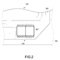
- Figure 2 illustrates an example of a conventional LED display 101 on the back of a control panel 100.
- a front support plate 200 is provided to a transmissive panel 102 and an LED device 307 is provided to the front support plate 200.
- the front support plate 200 can include a PCB, prepreg material, etc.
- the front support plate 200 and the LED device 307 add to the total thickness of the control panel 100.
- the control panel 100 is relatively thin in order to occupy less space in a device such as an appliance.
- FIG 3 illustrates a conventional LED device 307 that can be used in an LED display 101.
- the LED device 307 includes an LED chip 300 provided to a back support plate 202, and a light transmissive layer 304 provided to the back support plate 202 that covers the LED chip 300.
- a wire 303 can be connected to the LED chip 300 to supply electricity to the LED chip 300.
- the light transmissive layer 304 can be a material that diffuses light 701 emitted by the LED chip 300.
- the distance between the LED chip 300 and a light exit surface 302 is large enough for sufficient diffusion of light to result in substantial uniform illumination on the light exit surface 302. In some embodiments, the distance is about 0 to 5 mm in order to have substantial uniform illumination.
- the distance for substantial uniform illumination between the LED chip 300 and the light exit surface 302 also depends on the size and shape of a segment 1100 and location of the LED chip 300 within the segment 1100.
- a segment 1100 with a larger light exit surface 302 usually uses a larger distance for substantial uniform illumination.
- a segment 1100 with a more complex shape uses a larger distance for substantial uniform illumination.
- an LED chip 300 located off-center to the display segment 1100 uses a larger distance for substantial uniform illumination.
- the distance can also depend on the ability of the light transmissive layer 304 to diffuse the light 701 emitted by the LED chip 300.
- a light transmissive layer 304 that diffuses light more may be able to have a smaller distance than a light transmissive layer 304 that diffuses light less.
- the light transmissive layer 304 diffuses light more, less light 701 emitted by the LED chip 300 escapes the light exit surface 302. Therefore, even though the distance can be decreased by using a light transmissive layer 304 that diffuses light more, a more powerful LED chip 300 would be needed to produce the same amount of light 701 that escapes the light exit surface 302.
- Figure 4 illustrates one embodiment of an LED device 307 that includes an LED chip 300 provided to a back support plate 202, and a second support plate 400 provided to the back support plate 202.
- the second support plate 400 has a through-hole 401 of sufficient size and shape to accommodate the LED chip 300.
- a light transmissive layer 304 is provided to the second support plate 400 and covers the LED chip 300. As illustrated in Figure 4 , the light transmissive layer 304 can fill the through-hole 401 and surround the LED chip 300.
- the light transmissive layer 304 diffuses light.
- the light transmissive layer 304 can be a material that diffuses light 701 emitted by the LED chip 300. However, other options to diffuse the light can be used.
- the light transmissive layer 304 can be shaped like a lens. In another embodiment, the light transmissive layer 700 includes multiple layers. In a further embodiment, the light transmissive layer 304 can be opaque, semiopaque, frosty, clear, transparent, semitransparent, translucent, cloudy or a combination thereof. In other embodiments, the light transmissive layer 304 can have light transmissive properties graded in the layer. In one embodiment, the LED device 307 has the light transmissive layer 304 including air or a void. In some embodiments, the distance between the LED chip 300 and a light exit surface 302 is about 0 to 5 mm in order to have substantial uniform illumination.
- the distance 301 between the LED chip 300 and the light exit surface 302 is about the same for the conventional LED device 307 without a second support plate 400 in Figure 3 and the LED device 307 with a second support plate 400 in Figure 4 .
- the distance between the top surface 306 of the back support plate 202 and the light exit surface 302 is about the same.
- the distance between the top surface 306 of the back support plate 202 and the light exit surface 302 is greater than the distance between the top surface 404 of the second support plate 400 and the light exit surface 302.
- the second support plate 400 includes a through-hole 401
- the second support plate 400 adds to the structural integrity of the back support plate 202. Therefore, the thickness of the back support plate 202 can be less for an LED device 307 with a second support plate 400 than for an LED device 307 without the second support plate 400.
- the thickness of the back support plate without the second support plate 400 can be about the same as that of the combined thickness of the thickness of the back support plate 202 and thickness of the second support plate 400. Therefore, a control panel 100 with an LED device 307 with a second support plate 400 does not have to be thicker than a control panel 100 with an LED device without a second support plate 400.
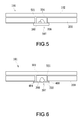
- Figure 5 and Figure 6 further illustrate the advantage of an LED display 101 with a second support plate 400.
- Figure 5 illustrates an LED display 101 including a conventional LED device 307 provided to a front support plate 200 with a through-hole 501.
- the light transmissive layer 304 of the LED device 307 substantially fills the through-hole 501 of the front support plate 200, and a portion of the top surface 306 of the back support plate 202 is provided to the front support plate 200.
- a light transmissive panel 102 can also be provided to the front support plate 200.
- the thickness of the front support plate 200 is about the same as the thickness of the light transmissive layer 304. Therefore, the thickness of the front support plate 200 is dependent on the thickness of the light transmissive layer 304. Since the thickness of the light transmissive layer 304 is relatively large to result in substantial uniform illumination, the front support plate board 200 is relatively thicker than for a control panel 100 without an LED display 101.
- FIG 6 illustrates one embodiment of an LED display 101 with a second support plate 400.
- the LED display 101 includes an LED device 307 provided to a front support plate 200 with a through-hole 501.
- a light transmissive layer 304 of the LED device substantially fills the through-hole 501 of the front support plate 200.
- a portion of the top surface 404 of the second support plate 400 is provided to the front support plate 200.
- a light transmissive panel 102 can also be provided to the front support plate 200.
- the distance between the top surface 404 of the second support plate 400 and the light exit surface 302 is less than the distance between the top surface 306 of the back support plate 202 and the light exit surface 302.
- the thickness of the front support plate 200 is dependent on the distance between the second support plate 400 and the exit light surface 302 for an LED display 101 with a second support plate 400.
- the thickness of the front support plate 200 is dependent on the distance between the top surface 306 of the back support plate 202 and the light exit surface 302. Therefore, the front support plate 200 can be thinner for an LED display 101 with a second support plate 400 than an LED display 101 without a second support plate 400.
- a thinner front support plate 200 is less expensive than a thicker front support plate 200; therefore, an LED display 101 with a second support plate 400 can be less expensive than an LED display 101 without a second support plate 400.
- the total thickness of an LED display 101 with a second support plate 400 can be less than an LED display without a second support plate 400.
- the thickness of the front support plate 200 is less for an LED display 101 with a second support plate 400.
- the total thickness of the back support plate 202 and the second support plate 400 for an LED display 101 with a second support plate 400 can be about the same as the thickness of the back support plate 202 for an LED display 101 without a second support plate. Therefore, an LED display 101 with a second support plate 400 can be advantageously used in applications requiring a thinner LED display 101 and at a reduced cost.
- an LED display 101 can further include a reflective layer.
- a reflective layer can be provided to the walls of the through-hole 501 of the front support plate 200, the walls of the through-hole 401 of the second support plate 400, the surface 306 of the back support plate 202, and/or the surface 404 of the second support plate 400.
- the reflective surface can be any material that reflects the light 701 emitted by the LED chip 300.
- the reflective layer can include a white material, metal film, etc.
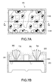
- Figures 7A-D illustrate a conventional LED display 101 with multiple segments 1100.
- Figures 7A-D illustrate a two seven-segment LED displays 101. Individual segments 1100 can be selectively illuminated to display up to two digital characters.
- Figure 7A illustrates a top view of the LED display 101
- Figure 7B illustrates a cross-sectional view of the LED display 101
- Figure 7C illustrates an individual segment 1100 from Figure 7A
- Figure 7D illustrates an individual segment 1100 from Figure 7B .
- an LED chip 300 is mounted to a back support plate 202
- a front support plate 200 is provided to the back support plate 202.
- the front support plate 200 includes through-holes 501 with both a size and shape to accommodate the LED chip 300 and light exit surface 302 with a desired size and shape. As discussed before for conventional LED displays 101, thickness of the front support plate 200 is dependent on the distance between the LED chip 300 and the light exit surface 302.
- Figures 8A-E and Figures 9A-B illustrate one embodiment of an LED display 101 with a second support plate 400.
- Figures 8A-E and Figures 9A-B illustrate a two seven-segment LED display 101 including individual segments 1100 that can be selectively illuminated to display up to two digital characters.
- Figure 8A illustrates a top view of the LED display 101
- Figure 8B and Figure 8C illustrate two side views of the LED display 101 which are perpendicular to each other.
- the side view in Figures 8B and 8C illustrate a back support plate 202 provided to a second support plate 400 and the second support plate 400 provided to a front support plate 200.
- Figure 8D illustrates area 800 of the LED display 101
- Figure 8E illustrates a cross-sectional of Figure 8D .
- FIG. 8E The cross-sectional view in Figure 8E is of a segment 1100 that can be selectively illuminated to represent a decimal point in the two seven-segment LED display 101.
- Figure 9A illustrates a front support plate 200, a back support plate 202 and a second support plate 400 while Figure 9B illustrates an assembled LED display 101.
- the three plates are stacked with the second support plate 400 between the front support plate 200 and the back support plate 202.
- the LED display 101 includes an LED chip 300 provided to the back support plate 202.
- the front support plate 200 can be a reflective material to increase the amount of light 701 emitted by the LED chip 300 to exit the light exit surface 302.
- the second support plate 400 includes a through-hole 401 for the LED chip 300 to reside.
- the front support plate 200 also has a through-hole 501 connected to the through-hole 401 of the second support plate 400. Size and shape of the second support plate through-hole 401 and the front support plate through-hole 501 may not be the same. In addition, size and shape may vary through the second support plate through-hole 401. Similarly, the size and shape may vary through the front support plate through-hole 501. For example, as illustrated in Figure 8E , the front support plate 200 includes a front support plate through-hole 501 that includes two different diameters. The size and shape of the front support plate through-hole 401 and the second support plate through-hole 401 can be designed so that a desired segment shape and a substantial uniform illumination across the segment shape can be achieved.
- the LED displays 101 in Figures 6 , 8A-E and 9A-B include a second support plate 400.
- the distance from the LED chip 300 and the light exit surface 302 is large enough to have substantial uniform illumination on the light exit surface. Therefore, an LED display 101 with a second support plate 400 can have a thinner front support plate 200.
- An LED display 101 with a second support plate 400 can reduce the thickness of the front support panel 200 by about the thickness of the second support plate 400.
- the thickness of the front support panel 200 of an LED display 101 with a second support plate 400 can be any thickness independent of the distance between the LED chip 300 and the light exit surface 302.
- the thickness of the front support panel 200 of an LED display 101 with a second support plate 400 is less than about 5 mm. More preferably, the thickness of the front support panel 200 of an LED display 101 with a second support plate 400 is less than about 2 mm. Most preferably, the thickness of the front support panel 200 of an LED display 101 with a second support plate 400 is less than about 1 mm.
- the first example compares LED displays including a distance between the LED chip 300 and the light exit surface of about 2 mm.
- the thickness of the front support plate 200 is about 2 mm.
- the thickness of a second support plate 400 can be about 1 mm while a thickness of a front support panel 200 can be about 1 mm. Therefore, the thickness of the front support panel 200 is about fifty percent that of an LED display 101 without a second support plate 400.
- the second example compares LED displays including a distance between the LED chip 300 and the light exit surface of about 5 mm, and also illustrates the increased benefits of an LED display 101 with a second support plate 400 as the distance between the LED chip 300 and the light exit surface increases.
- the thickness of the front support plate 200 is about 5 mm.
- the thickness of a second support plate 400 can be about 4 mm while a thickness of a front support panel 200 can be about 1 mm. Therefore, the thickness of the front support panel 200 is about twenty percent that of an LED display 101 without a second support plate 400.
- the thickness of the front support panel 200 can remain relatively thin even if the distance between the LED chip 300 and the light exit surface is relatively large. Therefore, as the distance for substantial uniform illumination between an LED chip 300 and a light exit surface 302 increases, the cost savings of using a second support plate 400 in an LED display 101 increases.
- a total thickness of an LED display 101 with a second support plate 400 can actually be less than that of a similar LED display 101 without a second support plate 400.
- a second support plate 400 adds structural integrity to the LED display 101. Therefore, the thickness of the back support plate 202 can be reduced as well.
- the thickness of the back support plate 202 can be reduced, for example, to 1 mm. Therefore, in this example, the total thickness of an LED display 101 with a second support plate 400 is about 1 mm less than the total thickness of an LED display 101 without a second support plate 400.
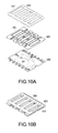
- Figures 10A-B illustrate one embodiment of an LED display 101 with five segments 1100.
- Figure 10A illustrates a front support plate 200, a back support plate 202 and a second support plate 400 while Figure 10B illustrates an assembled LED display 101.
- the back support plate 202 in Figure 10A includes a dashed circuit pattern to illustrate that the back support plate 202 can be a printed circuit board, but the dashed circuit pattern is not intended to show a specific circuit.
- the three plates are stacked with the second support plate 400 between the front support plate 200 and the back support plate 202.
- the back support plate 202 has LED chips 300 provided.
- the second support plate 400 is provided to the back support plate 202 and includes through-holes 401 above the LED chips 300.
- the front support plate 200 is provided to the second support plate 400 and includes through-holes 501.
- the front support plate through-holes 501 are connected to the second support plate through-holes 401.
- the front support plate through-holes 501 and second support plate through-holes 401 are substantially filled with a light transmissive layer 304.
- Light emitted by the LED chip 300 exits at an exit light surface 302.
- the distance between the LED chip 300 and the exit light surface 302 is sufficient in order for the exit light surface 302 of each segment 1100 to produce substantially uniform illumination when the LED chip 300 is activated.
- Figures 11A-E illustrate one embodiment of an LED display 101 that includes more than one LED chip 300 within a single segment 1100.
- Figure 11A illustrates a top view of the LED display 101 along with cross-sectional views A-A and B-B in Figure 11B and Figure 11C , respectively.
- Figure 11D illustrates an enlarged top view of Figure 11A
- Figure 11E illustrates a B-B cross-section view.
- An LED chip 300 is provided to a back support plate 202.
- the back support plate 202 is provided to a second support plate 400.
- the second support plate 400 includes a through-hole 401 wherein the LED chips 300 reside.
- a reflector 1002 can be provided to the interior walls of the through-hole 401 of the second support plate 400.
- the through-hole 401 can be substantially filled with a light transmissive layer 304.
- the light transmissive layer 304 can be a material that diffuses light.
- the second support plate 400 can also be provided to a front support plate 200 or a light transmissive panel 102. If a front support plate 200 is provided to the second support plate 400, a light transmissive panel 102 can be provided to the front support plate 200.
- An LED display 101 with a second support plate 400 can be manufactured in a number of methods.
- an LED chip 300 is provided to a back support plate 202.
- a through-hole 401 is formed in a second support plate 400.
- the through-hole 401 can be formed by methods including drilling, punching, machining, or etc.
- the second support plate 400 is provided to the back support plate 202.
- the second support plate 400 and the back support plate 202 can be provided by methods including adhesives, glues, or etc.
- a through-hole 501 is formed in a front support plate 200.
- the through-hole 501 can be formed by methods including drilling, punching, machining, or etc.
- a portion of the second support plate 400 is provided to a front support plate 200.
- a light transmissive layer 304 is provided into the through-hole 401 of the second support plate 400 and the through-hole 501 of the front support plate 200.
- the light transmissive layer 304 diffuses light.
- the light transmissive layer 304 can be a material that diffuses light 701 emitted by the LED chip 300. However, other options to diffuse the light can be used.
- the light transmissive layer 304 can be shaped like a lens.
- the light transmissive layer 700 includes multiple layers.
- the light transmissive layer 304 can be opaque, semiopaque, frosty, clear, transparent, semitransparent, translucent, cloudy or a combination thereof.
- the light transmissive layer 304 can have light transmissive properties graded in the layer.
- the LED device 307 has the light transmissive layer 304 including air or a void.
- a through-hole 501 is formed in a front support plate 200.
- the front support plate 200 is provided to a light transmissive panel 102.
- An LED chip 300 is provided to a back support plate 202.
- a through-hole 401 is formed in a second support plate 400, and the second support plate 400 is provided to the back support plate 202 so that the LED chip is in the through-hole 401 of the second support plate.
- the through-hole 501 of the front support plate 200 is substantially filled with a light transmissive layer 304.
- a portion of the second support plate 400 is provided to the front support plate 200.
- a back support plate 202 is provided to a second support plate 400.
- the second support plate 400 is provided to a front support plate 200.
- a hole is formed through the front support plate 200 and the second support plate 400.
- the hole forms a through-hole 501 in the front support plate 200 and a through-hole 401 in the second support plate 400.
- the hole can be formed by methods including drilling, punching, machining, or etc.
- An LED chip 300 is provided to the back support plate 200 in the hole.
- a light transmissive layer 304 is provided into the through-hole 501 of the front support plate 200 and the through-hole 401 in the second support plate 400.
- a light transmissive panel 102 is provided to the front support plate 200.
- a back support plate 202 is provided to a front support plate 200 without a second support plate 400.
- a hole is formed through the front support plate 200 and partially though the back support plate 400.
- the hole forms a though hole 501 in the front support plate 200 and forms a through-hole 401 in a quasi second support plate 400.
- the portion of the back support plate 202 that the hole is formed in forms the second support plate 400.
- the portion of the back support plate 202 that the hole is not formed remains the back support plate 202.
- An LED chip 300 is provided to the back support plate 200 in the hole.
- LED display 101 Although various embodiments have been described above, other embodiments will be within the skill of one of ordinary skill in the art. Thus, for example, although described primarily in terms of an LED display 101, one of ordinary skill in the art will recognize that all or part of the LED display 101 can be applied to other light emitting devices, such as, for example, lasers, field emission devices, and filament light devices, and organic LEDs. Thus, the invention is limited only by the claims that follow.
Landscapes
- Physics & Mathematics (AREA)
- General Physics & Mathematics (AREA)
- Engineering & Computer Science (AREA)
- Theoretical Computer Science (AREA)
- Devices For Indicating Variable Information By Combining Individual Elements (AREA)
- Illuminated Signs And Luminous Advertising (AREA)
- Led Device Packages (AREA)
Applications Claiming Priority (1)
| Application Number | Priority Date | Filing Date | Title |
|---|---|---|---|
| US12/269,846 US8136960B2 (en) | 2008-11-12 | 2008-11-12 | Light emitting diode display |
Publications (3)
| Publication Number | Publication Date |
|---|---|
| EP2187374A2 true EP2187374A2 (de) | 2010-05-19 |
| EP2187374A3 EP2187374A3 (de) | 2010-08-04 |
| EP2187374B1 EP2187374B1 (de) | 2012-01-18 |
Family
ID=41698251
Family Applications (1)
| Application Number | Title | Priority Date | Filing Date |
|---|---|---|---|
| EP09175378A Not-in-force EP2187374B1 (de) | 2008-11-12 | 2009-11-09 | Lichtemittierende Diodenanzeige |
Country Status (3)
| Country | Link |
|---|---|
| US (2) | US8136960B2 (de) |
| EP (1) | EP2187374B1 (de) |
| AT (1) | ATE542211T1 (de) |
Cited By (1)
| Publication number | Priority date | Publication date | Assignee | Title |
|---|---|---|---|---|
| WO2025252430A1 (de) * | 2024-06-04 | 2025-12-11 | Ams-Osram International Gmbh | Leuchtvorrichtung und verfahren zur herstellung einer leuchtvorrichtung |
Families Citing this family (7)
| Publication number | Priority date | Publication date | Assignee | Title |
|---|---|---|---|---|
| US8136960B2 (en) * | 2008-11-12 | 2012-03-20 | American Opto Plus Led Corporation | Light emitting diode display |
| US7952106B2 (en) * | 2009-04-10 | 2011-05-31 | Everlight Electronics Co., Ltd. | Light emitting diode device having uniform current distribution and method for forming the same |
| DE102011114741B3 (de) * | 2011-09-28 | 2012-12-13 | E.G.O. Elektro-Gerätebau GmbH | Anzeigevorrichtung, Elektrogerät und Verfahren zur Anzeige |
| US9220394B2 (en) * | 2013-08-15 | 2015-12-29 | Whirlpool Corporation | LED console assembly with light reflector |
| US9982866B2 (en) * | 2013-10-29 | 2018-05-29 | Whirlpool Corporation | Console assembly with integrated light reflector cups |
| US10952315B2 (en) | 2019-07-29 | 2021-03-16 | Haier Us Appliance Solutions, Inc. | Light blocking features for indicator lights in an appliance |
| US10753597B1 (en) | 2019-07-29 | 2020-08-25 | Haier Us Appliance Solutions, Inc. | Light blocking features for indicator lights in an appliance |
Family Cites Families (24)
| Publication number | Priority date | Publication date | Assignee | Title |
|---|---|---|---|---|
| US1998857A (en) * | 1933-03-27 | 1935-04-23 | Wolff Hendrik | Illuminated sign for day and night display |
| US3918053A (en) * | 1972-07-03 | 1975-11-04 | Dialight Corp | Digital display |
| US4146883A (en) * | 1977-09-12 | 1979-03-27 | Minnesota Mining And Manufacturing Company | Display |
| DE3633203A1 (de) * | 1986-09-30 | 1988-03-31 | Siemens Ag | Lichtemissionsdioden (led) - anzeigevorrichtung |
| US4914731A (en) | 1987-08-12 | 1990-04-03 | Chen Shen Yuan | Quickly formed light emitting diode display and a method for forming the same |
| US4843280A (en) * | 1988-01-15 | 1989-06-27 | Siemens Corporate Research & Support, Inc. | A modular surface mount component for an electrical device or led's |
| US5331512A (en) * | 1992-04-16 | 1994-07-19 | Orton Kevin R | Surface-mount LED |
| JP3565451B2 (ja) | 1995-07-06 | 2004-09-15 | 株式会社Mrd | ディジタル表示器 |
| JP4082768B2 (ja) | 1997-12-04 | 2008-04-30 | 株式会社キーエンス | 表示器 |
| US6307527B1 (en) * | 1998-07-27 | 2001-10-23 | John S. Youngquist | LED display assembly |
| US6829582B1 (en) * | 2000-10-10 | 2004-12-07 | International Business Machines Corporation | Controlled access to audio signals based on objectionable audio content detected via sound recognition |
| US6631575B1 (en) | 2000-11-08 | 2003-10-14 | Daktronics, Inc. | LED and light diffuser for a lighted sign |
| EP1387412B1 (de) * | 2001-04-12 | 2009-03-11 | Matsushita Electric Works, Ltd. | Lichtquellenbauelement mit led und verfahren zu seiner herstellung |
| JP4703903B2 (ja) * | 2001-07-17 | 2011-06-15 | ローム株式会社 | 半導体装置の製造方法および半導体装置 |
| JP4045781B2 (ja) * | 2001-08-28 | 2008-02-13 | 松下電工株式会社 | 発光装置 |
| US6810612B2 (en) * | 2001-12-11 | 2004-11-02 | Agon-Tech. Corporation | Signboard structure enabling quick and detachable assembling of a face panel thereof |
| TW558775B (en) * | 2002-06-27 | 2003-10-21 | Solidlite Corp | Package of compound type LED |
| US7850339B2 (en) * | 2003-01-30 | 2010-12-14 | Touchsensor Technologies, Llc | Display having thin cross-section and/or multi-colored output |
| US7175304B2 (en) * | 2003-01-30 | 2007-02-13 | Touchsensor Technologies, Llc | Integrated low profile display |
| JP4922555B2 (ja) * | 2004-09-24 | 2012-04-25 | スタンレー電気株式会社 | Led装置 |
| CN2899005Y (zh) * | 2004-12-06 | 2007-05-09 | 贺伟 | 一种led显示装置 |
| JP2007156228A (ja) * | 2005-12-07 | 2007-06-21 | Rohm Co Ltd | Led表示器 |
| US8136960B2 (en) * | 2008-11-12 | 2012-03-20 | American Opto Plus Led Corporation | Light emitting diode display |
| US8235548B2 (en) * | 2008-11-12 | 2012-08-07 | American Opto Plus Led Corporation | Light emitting diode display |
-
2008
- 2008-11-12 US US12/269,846 patent/US8136960B2/en active Active
-
2009
- 2009-11-09 EP EP09175378A patent/EP2187374B1/de not_active Not-in-force
- 2009-11-09 AT AT09175378T patent/ATE542211T1/de active
-
2012
- 2012-02-13 US US13/372,331 patent/US8328389B2/en active Active
Non-Patent Citations (1)
| Title |
|---|
| None |
Cited By (1)
| Publication number | Priority date | Publication date | Assignee | Title |
|---|---|---|---|---|
| WO2025252430A1 (de) * | 2024-06-04 | 2025-12-11 | Ams-Osram International Gmbh | Leuchtvorrichtung und verfahren zur herstellung einer leuchtvorrichtung |
Also Published As
| Publication number | Publication date |
|---|---|
| EP2187374B1 (de) | 2012-01-18 |
| US8328389B2 (en) | 2012-12-11 |
| US20120140485A1 (en) | 2012-06-07 |
| US20100118529A1 (en) | 2010-05-13 |
| ATE542211T1 (de) | 2012-02-15 |
| US8136960B2 (en) | 2012-03-20 |
| EP2187374A3 (de) | 2010-08-04 |
Similar Documents
| Publication | Publication Date | Title |
|---|---|---|
| US8328389B2 (en) | Light emitting diode display | |
| JP4825165B2 (ja) | 表示装置 | |
| US7175304B2 (en) | Integrated low profile display | |
| KR101469293B1 (ko) | 얇은 단면 및/또는 멀티-컬러 출력을 갖는 디스플레이 | |
| US7607808B2 (en) | Instrument panel housing with light diffuser | |
| JPWO2007123202A1 (ja) | 表示装置およびその製造方法、パターン表示方法、ならびにブラインド装置およびブラインド方法 | |
| US20060227545A1 (en) | Light emitting panel | |
| JP2015195413A (ja) | 一体的に形成された一体成形発光ダイオード光ワイヤー及びその使用 | |
| EP2765485A1 (de) | Leuchtende Tastatur und Lichtleiterplatte dafür | |
| US6502946B1 (en) | Planar display lamp and method of forming a light scatterer pattern | |
| JP2008203633A (ja) | 表示装置 | |
| JP2007156228A (ja) | Led表示器 | |
| JP3267119B2 (ja) | Led面光源 | |
| US8235548B2 (en) | Light emitting diode display | |
| JP4785021B2 (ja) | 7セグメントled数字表示器およびその製造方法 | |
| JPWO2003075249A1 (ja) | 表示装置およびその光源 | |
| EP4100939B1 (de) | Bis zur beleuchtung verborgene anzeigetafel und anzeigeanordnung damit | |
| US20060039129A1 (en) | Backlight using reversely mounted LEDs | |
| JP6915199B2 (ja) | 発光表示装置 | |
| JP4386778B2 (ja) | 自動販売機の商品サンプル照明装置 | |
| CN201707850U (zh) | 发光显示器 | |
| KR200462966Y1 (ko) | 발광 다이오드 디스플레이 | |
| JP2012084425A (ja) | 照明装置 | |
| JP3160220U (ja) | Led表示装置 | |
| CN217004133U (zh) | 一种边界分明光线柔和的吉他灯 |
Legal Events
| Date | Code | Title | Description |
|---|---|---|---|
| PUAI | Public reference made under article 153(3) epc to a published international application that has entered the european phase |
Free format text: ORIGINAL CODE: 0009012 |
|
| AK | Designated contracting states |
Kind code of ref document: A2 Designated state(s): AT BE BG CH CY CZ DE DK EE ES FI FR GB GR HR HU IE IS IT LI LT LU LV MC MK MT NL NO PL PT RO SE SI SK SM TR |
|
| AX | Request for extension of the european patent |
Extension state: AL BA RS |
|
| PUAL | Search report despatched |
Free format text: ORIGINAL CODE: 0009013 |
|
| AK | Designated contracting states |
Kind code of ref document: A3 Designated state(s): AT BE BG CH CY CZ DE DK EE ES FI FR GB GR HR HU IE IS IT LI LT LU LV MC MK MT NL NO PL PT RO SE SI SK SM TR |
|
| AX | Request for extension of the european patent |
Extension state: AL BA RS |
|
| 17P | Request for examination filed |
Effective date: 20110204 |
|
| GRAP | Despatch of communication of intention to grant a patent |
Free format text: ORIGINAL CODE: EPIDOSNIGR1 |
|
| RIC1 | Information provided on ipc code assigned before grant |
Ipc: G09F 9/33 20060101AFI20110530BHEP |
|
| GRAS | Grant fee paid |
Free format text: ORIGINAL CODE: EPIDOSNIGR3 |
|
| GRAA | (expected) grant |
Free format text: ORIGINAL CODE: 0009210 |
|
| AK | Designated contracting states |
Kind code of ref document: B1 Designated state(s): AT BE BG CH CY CZ DE DK EE ES FI FR GB GR HR HU IE IS IT LI LT LU LV MC MK MT NL NO PL PT RO SE SI SK SM TR |
|
| REG | Reference to a national code |
Ref country code: GB Ref legal event code: FG4D |
|
| REG | Reference to a national code |
Ref country code: CH Ref legal event code: EP |
|
| REG | Reference to a national code |
Ref country code: IE Ref legal event code: FG4D Ref country code: AT Ref legal event code: REF Ref document number: 542211 Country of ref document: AT Kind code of ref document: T Effective date: 20120215 |
|
| REG | Reference to a national code |
Ref country code: DE Ref legal event code: R096 Ref document number: 602009004721 Country of ref document: DE Effective date: 20120322 |
|
| REG | Reference to a national code |
Ref country code: NL Ref legal event code: VDEP Effective date: 20120118 |
|
| LTIE | Lt: invalidation of european patent or patent extension |
Effective date: 20120118 |
|
| PG25 | Lapsed in a contracting state [announced via postgrant information from national office to epo] |
Ref country code: NL Free format text: LAPSE BECAUSE OF FAILURE TO SUBMIT A TRANSLATION OF THE DESCRIPTION OR TO PAY THE FEE WITHIN THE PRESCRIBED TIME-LIMIT Effective date: 20120118 Ref country code: BE Free format text: LAPSE BECAUSE OF FAILURE TO SUBMIT A TRANSLATION OF THE DESCRIPTION OR TO PAY THE FEE WITHIN THE PRESCRIBED TIME-LIMIT Effective date: 20120118 Ref country code: BG Free format text: LAPSE BECAUSE OF FAILURE TO SUBMIT A TRANSLATION OF THE DESCRIPTION OR TO PAY THE FEE WITHIN THE PRESCRIBED TIME-LIMIT Effective date: 20120418 Ref country code: IS Free format text: LAPSE BECAUSE OF FAILURE TO SUBMIT A TRANSLATION OF THE DESCRIPTION OR TO PAY THE FEE WITHIN THE PRESCRIBED TIME-LIMIT Effective date: 20120518 Ref country code: LT Free format text: LAPSE BECAUSE OF FAILURE TO SUBMIT A TRANSLATION OF THE DESCRIPTION OR TO PAY THE FEE WITHIN THE PRESCRIBED TIME-LIMIT Effective date: 20120118 Ref country code: HR Free format text: LAPSE BECAUSE OF FAILURE TO SUBMIT A TRANSLATION OF THE DESCRIPTION OR TO PAY THE FEE WITHIN THE PRESCRIBED TIME-LIMIT Effective date: 20120118 Ref country code: NO Free format text: LAPSE BECAUSE OF FAILURE TO SUBMIT A TRANSLATION OF THE DESCRIPTION OR TO PAY THE FEE WITHIN THE PRESCRIBED TIME-LIMIT Effective date: 20120418 |
|
| PG25 | Lapsed in a contracting state [announced via postgrant information from national office to epo] |
Ref country code: PL Free format text: LAPSE BECAUSE OF FAILURE TO SUBMIT A TRANSLATION OF THE DESCRIPTION OR TO PAY THE FEE WITHIN THE PRESCRIBED TIME-LIMIT Effective date: 20120118 Ref country code: PT Free format text: LAPSE BECAUSE OF FAILURE TO SUBMIT A TRANSLATION OF THE DESCRIPTION OR TO PAY THE FEE WITHIN THE PRESCRIBED TIME-LIMIT Effective date: 20120518 Ref country code: GR Free format text: LAPSE BECAUSE OF FAILURE TO SUBMIT A TRANSLATION OF THE DESCRIPTION OR TO PAY THE FEE WITHIN THE PRESCRIBED TIME-LIMIT Effective date: 20120419 Ref country code: FI Free format text: LAPSE BECAUSE OF FAILURE TO SUBMIT A TRANSLATION OF THE DESCRIPTION OR TO PAY THE FEE WITHIN THE PRESCRIBED TIME-LIMIT Effective date: 20120118 Ref country code: LV Free format text: LAPSE BECAUSE OF FAILURE TO SUBMIT A TRANSLATION OF THE DESCRIPTION OR TO PAY THE FEE WITHIN THE PRESCRIBED TIME-LIMIT Effective date: 20120118 |
|
| REG | Reference to a national code |
Ref country code: AT Ref legal event code: MK05 Ref document number: 542211 Country of ref document: AT Kind code of ref document: T Effective date: 20120118 |
|
| PG25 | Lapsed in a contracting state [announced via postgrant information from national office to epo] |
Ref country code: CY Free format text: LAPSE BECAUSE OF FAILURE TO SUBMIT A TRANSLATION OF THE DESCRIPTION OR TO PAY THE FEE WITHIN THE PRESCRIBED TIME-LIMIT Effective date: 20120118 |
|
| PG25 | Lapsed in a contracting state [announced via postgrant information from national office to epo] |
Ref country code: SI Free format text: LAPSE BECAUSE OF FAILURE TO SUBMIT A TRANSLATION OF THE DESCRIPTION OR TO PAY THE FEE WITHIN THE PRESCRIBED TIME-LIMIT Effective date: 20120118 Ref country code: EE Free format text: LAPSE BECAUSE OF FAILURE TO SUBMIT A TRANSLATION OF THE DESCRIPTION OR TO PAY THE FEE WITHIN THE PRESCRIBED TIME-LIMIT Effective date: 20120118 Ref country code: CZ Free format text: LAPSE BECAUSE OF FAILURE TO SUBMIT A TRANSLATION OF THE DESCRIPTION OR TO PAY THE FEE WITHIN THE PRESCRIBED TIME-LIMIT Effective date: 20120118 Ref country code: DK Free format text: LAPSE BECAUSE OF FAILURE TO SUBMIT A TRANSLATION OF THE DESCRIPTION OR TO PAY THE FEE WITHIN THE PRESCRIBED TIME-LIMIT Effective date: 20120118 Ref country code: RO Free format text: LAPSE BECAUSE OF FAILURE TO SUBMIT A TRANSLATION OF THE DESCRIPTION OR TO PAY THE FEE WITHIN THE PRESCRIBED TIME-LIMIT Effective date: 20120118 Ref country code: SE Free format text: LAPSE BECAUSE OF FAILURE TO SUBMIT A TRANSLATION OF THE DESCRIPTION OR TO PAY THE FEE WITHIN THE PRESCRIBED TIME-LIMIT Effective date: 20120118 |
|
| PLBE | No opposition filed within time limit |
Free format text: ORIGINAL CODE: 0009261 |
|
| STAA | Information on the status of an ep patent application or granted ep patent |
Free format text: STATUS: NO OPPOSITION FILED WITHIN TIME LIMIT |
|
| PG25 | Lapsed in a contracting state [announced via postgrant information from national office to epo] |
Ref country code: SK Free format text: LAPSE BECAUSE OF FAILURE TO SUBMIT A TRANSLATION OF THE DESCRIPTION OR TO PAY THE FEE WITHIN THE PRESCRIBED TIME-LIMIT Effective date: 20120118 |
|
| 26N | No opposition filed |
Effective date: 20121019 |
|
| PG25 | Lapsed in a contracting state [announced via postgrant information from national office to epo] |
Ref country code: AT Free format text: LAPSE BECAUSE OF FAILURE TO SUBMIT A TRANSLATION OF THE DESCRIPTION OR TO PAY THE FEE WITHIN THE PRESCRIBED TIME-LIMIT Effective date: 20120118 |
|
| REG | Reference to a national code |
Ref country code: DE Ref legal event code: R097 Ref document number: 602009004721 Country of ref document: DE Effective date: 20121019 |
|
| PG25 | Lapsed in a contracting state [announced via postgrant information from national office to epo] |
Ref country code: ES Free format text: LAPSE BECAUSE OF FAILURE TO SUBMIT A TRANSLATION OF THE DESCRIPTION OR TO PAY THE FEE WITHIN THE PRESCRIBED TIME-LIMIT Effective date: 20120429 |
|
| REG | Reference to a national code |
Ref country code: IE Ref legal event code: MM4A |
|
| PG25 | Lapsed in a contracting state [announced via postgrant information from national office to epo] |
Ref country code: IE Free format text: LAPSE BECAUSE OF NON-PAYMENT OF DUE FEES Effective date: 20121109 |
|
| PG25 | Lapsed in a contracting state [announced via postgrant information from national office to epo] |
Ref country code: MT Free format text: LAPSE BECAUSE OF FAILURE TO SUBMIT A TRANSLATION OF THE DESCRIPTION OR TO PAY THE FEE WITHIN THE PRESCRIBED TIME-LIMIT Effective date: 20120118 |
|
| PGFP | Annual fee paid to national office [announced via postgrant information from national office to epo] |
Ref country code: DE Payment date: 20131130 Year of fee payment: 5 Ref country code: FR Payment date: 20131119 Year of fee payment: 5 |
|
| PGFP | Annual fee paid to national office [announced via postgrant information from national office to epo] |
Ref country code: TR Payment date: 20131101 Year of fee payment: 5 |
|
| PG25 | Lapsed in a contracting state [announced via postgrant information from national office to epo] |
Ref country code: MC Free format text: LAPSE BECAUSE OF NON-PAYMENT OF DUE FEES Effective date: 20121130 |
|
| PG25 | Lapsed in a contracting state [announced via postgrant information from national office to epo] |
Ref country code: SM Free format text: LAPSE BECAUSE OF FAILURE TO SUBMIT A TRANSLATION OF THE DESCRIPTION OR TO PAY THE FEE WITHIN THE PRESCRIBED TIME-LIMIT Effective date: 20120118 Ref country code: LU Free format text: LAPSE BECAUSE OF NON-PAYMENT OF DUE FEES Effective date: 20121109 |
|
| REG | Reference to a national code |
Ref country code: CH Ref legal event code: PL |
|
| PG25 | Lapsed in a contracting state [announced via postgrant information from national office to epo] |
Ref country code: CH Free format text: LAPSE BECAUSE OF NON-PAYMENT OF DUE FEES Effective date: 20131130 Ref country code: HU Free format text: LAPSE BECAUSE OF FAILURE TO SUBMIT A TRANSLATION OF THE DESCRIPTION OR TO PAY THE FEE WITHIN THE PRESCRIBED TIME-LIMIT Effective date: 20091109 Ref country code: LI Free format text: LAPSE BECAUSE OF NON-PAYMENT OF DUE FEES Effective date: 20131130 |
|
| REG | Reference to a national code |
Ref country code: DE Ref legal event code: R119 Ref document number: 602009004721 Country of ref document: DE |
|
| PG25 | Lapsed in a contracting state [announced via postgrant information from national office to epo] |
Ref country code: MK Free format text: LAPSE BECAUSE OF FAILURE TO SUBMIT A TRANSLATION OF THE DESCRIPTION OR TO PAY THE FEE WITHIN THE PRESCRIBED TIME-LIMIT Effective date: 20120118 |
|
| REG | Reference to a national code |
Ref country code: FR Ref legal event code: ST Effective date: 20150731 |
|
| PG25 | Lapsed in a contracting state [announced via postgrant information from national office to epo] |
Ref country code: DE Free format text: LAPSE BECAUSE OF NON-PAYMENT OF DUE FEES Effective date: 20150602 |
|
| PG25 | Lapsed in a contracting state [announced via postgrant information from national office to epo] |
Ref country code: FR Free format text: LAPSE BECAUSE OF NON-PAYMENT OF DUE FEES Effective date: 20141201 |
|
| PGFP | Annual fee paid to national office [announced via postgrant information from national office to epo] |
Ref country code: GB Payment date: 20151123 Year of fee payment: 7 Ref country code: IT Payment date: 20151124 Year of fee payment: 7 |
|
| GBPC | Gb: european patent ceased through non-payment of renewal fee |
Effective date: 20161109 |
|
| PG25 | Lapsed in a contracting state [announced via postgrant information from national office to epo] |
Ref country code: TR Free format text: LAPSE BECAUSE OF NON-PAYMENT OF DUE FEES Effective date: 20141109 |
|
| PG25 | Lapsed in a contracting state [announced via postgrant information from national office to epo] |
Ref country code: IT Free format text: LAPSE BECAUSE OF NON-PAYMENT OF DUE FEES Effective date: 20161109 |
|
| PG25 | Lapsed in a contracting state [announced via postgrant information from national office to epo] |
Ref country code: GB Free format text: LAPSE BECAUSE OF NON-PAYMENT OF DUE FEES Effective date: 20161109 |