EP2187440A2 - Matériau à radiation de chaleur, dispositif électronique et procédé de fabrication du dispositif électronique - Google Patents
Matériau à radiation de chaleur, dispositif électronique et procédé de fabrication du dispositif électronique Download PDFInfo
- Publication number
- EP2187440A2 EP2187440A2 EP20090173510 EP09173510A EP2187440A2 EP 2187440 A2 EP2187440 A2 EP 2187440A2 EP 20090173510 EP20090173510 EP 20090173510 EP 09173510 A EP09173510 A EP 09173510A EP 2187440 A2 EP2187440 A2 EP 2187440A2
- Authority
- EP
- European Patent Office
- Prior art keywords
- heat
- carbon nanotube
- thermoplastic resin
- nanotube sheet
- carbon nanotubes
- Prior art date
- Legal status (The legal status is an assumption and is not a legal conclusion. Google has not performed a legal analysis and makes no representation as to the accuracy of the status listed.)
- Granted
Links
Images








Classifications
-
- H—ELECTRICITY
- H10—SEMICONDUCTOR DEVICES; ELECTRIC SOLID-STATE DEVICES NOT OTHERWISE PROVIDED FOR
- H10W—GENERIC PACKAGES, INTERCONNECTIONS, CONNECTORS OR OTHER CONSTRUCTIONAL DETAILS OF DEVICES COVERED BY CLASS H10
- H10W40/00—Arrangements for thermal protection or thermal control
- H10W40/70—Fillings or auxiliary members in containers or in encapsulations for thermal protection or control
- H10W40/77—Auxiliary members characterised by their shape
-
- F—MECHANICAL ENGINEERING; LIGHTING; HEATING; WEAPONS; BLASTING
- F28—HEAT EXCHANGE IN GENERAL
- F28F—DETAILS OF HEAT-EXCHANGE AND HEAT-TRANSFER APPARATUS, OF GENERAL APPLICATION
- F28F3/00—Plate-like or laminated elements; Assemblies of plate-like or laminated elements
- F28F3/02—Elements or assemblies thereof with means for increasing heat-transfer area, e.g. with fins, with recesses, with corrugations
- F28F3/022—Elements or assemblies thereof with means for increasing heat-transfer area, e.g. with fins, with recesses, with corrugations the means being wires or pins
-
- H—ELECTRICITY
- H10—SEMICONDUCTOR DEVICES; ELECTRIC SOLID-STATE DEVICES NOT OTHERWISE PROVIDED FOR
- H10W—GENERIC PACKAGES, INTERCONNECTIONS, CONNECTORS OR OTHER CONSTRUCTIONAL DETAILS OF DEVICES COVERED BY CLASS H10
- H10W40/00—Arrangements for thermal protection or thermal control
- H10W40/20—Arrangements for cooling
- H10W40/25—Arrangements for cooling characterised by their materials
-
- H—ELECTRICITY
- H10—SEMICONDUCTOR DEVICES; ELECTRIC SOLID-STATE DEVICES NOT OTHERWISE PROVIDED FOR
- H10W—GENERIC PACKAGES, INTERCONNECTIONS, CONNECTORS OR OTHER CONSTRUCTIONAL DETAILS OF DEVICES COVERED BY CLASS H10
- H10W72/00—Interconnections or connectors in packages
- H10W72/30—Die-attach connectors
-
- H—ELECTRICITY
- H10—SEMICONDUCTOR DEVICES; ELECTRIC SOLID-STATE DEVICES NOT OTHERWISE PROVIDED FOR
- H10W—GENERIC PACKAGES, INTERCONNECTIONS, CONNECTORS OR OTHER CONSTRUCTIONAL DETAILS OF DEVICES COVERED BY CLASS H10
- H10W40/00—Arrangements for thermal protection or thermal control
- H10W40/20—Arrangements for cooling
- H10W40/25—Arrangements for cooling characterised by their materials
- H10W40/257—Arrangements for cooling characterised by their materials having a heterogeneous or anisotropic structure, e.g. powder or fibres in a matrix, wire mesh or porous structures
-
- H—ELECTRICITY
- H10—SEMICONDUCTOR DEVICES; ELECTRIC SOLID-STATE DEVICES NOT OTHERWISE PROVIDED FOR
- H10W—GENERIC PACKAGES, INTERCONNECTIONS, CONNECTORS OR OTHER CONSTRUCTIONAL DETAILS OF DEVICES COVERED BY CLASS H10
- H10W72/00—Interconnections or connectors in packages
- H10W72/30—Die-attach connectors
- H10W72/321—Structures or relative sizes of die-attach connectors
- H10W72/325—Die-attach connectors having a filler embedded in a matrix
-
- H—ELECTRICITY
- H10—SEMICONDUCTOR DEVICES; ELECTRIC SOLID-STATE DEVICES NOT OTHERWISE PROVIDED FOR
- H10W—GENERIC PACKAGES, INTERCONNECTIONS, CONNECTORS OR OTHER CONSTRUCTIONAL DETAILS OF DEVICES COVERED BY CLASS H10
- H10W72/00—Interconnections or connectors in packages
- H10W72/30—Die-attach connectors
- H10W72/351—Materials of die-attach connectors
-
- H—ELECTRICITY
- H10—SEMICONDUCTOR DEVICES; ELECTRIC SOLID-STATE DEVICES NOT OTHERWISE PROVIDED FOR
- H10W—GENERIC PACKAGES, INTERCONNECTIONS, CONNECTORS OR OTHER CONSTRUCTIONAL DETAILS OF DEVICES COVERED BY CLASS H10
- H10W72/00—Interconnections or connectors in packages
- H10W72/851—Dispositions of multiple connectors or interconnections
- H10W72/874—On different surfaces
- H10W72/877—Bump connectors and die-attach connectors
-
- H—ELECTRICITY
- H10—SEMICONDUCTOR DEVICES; ELECTRIC SOLID-STATE DEVICES NOT OTHERWISE PROVIDED FOR
- H10W—GENERIC PACKAGES, INTERCONNECTIONS, CONNECTORS OR OTHER CONSTRUCTIONAL DETAILS OF DEVICES COVERED BY CLASS H10
- H10W72/00—Interconnections or connectors in packages
- H10W72/90—Bond pads, in general
- H10W72/931—Shapes of bond pads
-
- H—ELECTRICITY
- H10—SEMICONDUCTOR DEVICES; ELECTRIC SOLID-STATE DEVICES NOT OTHERWISE PROVIDED FOR
- H10W—GENERIC PACKAGES, INTERCONNECTIONS, CONNECTORS OR OTHER CONSTRUCTIONAL DETAILS OF DEVICES COVERED BY CLASS H10
- H10W90/00—Package configurations
- H10W90/701—Package configurations characterised by the relative positions of pads or connectors relative to package parts
- H10W90/721—Package configurations characterised by the relative positions of pads or connectors relative to package parts of bump connectors
- H10W90/724—Package configurations characterised by the relative positions of pads or connectors relative to package parts of bump connectors between a chip and a stacked insulating package substrate, interposer or RDL
-
- Y—GENERAL TAGGING OF NEW TECHNOLOGICAL DEVELOPMENTS; GENERAL TAGGING OF CROSS-SECTIONAL TECHNOLOGIES SPANNING OVER SEVERAL SECTIONS OF THE IPC; TECHNICAL SUBJECTS COVERED BY FORMER USPC CROSS-REFERENCE ART COLLECTIONS [XRACs] AND DIGESTS
- Y10—TECHNICAL SUBJECTS COVERED BY FORMER USPC
- Y10S—TECHNICAL SUBJECTS COVERED BY FORMER USPC CROSS-REFERENCE ART COLLECTIONS [XRACs] AND DIGESTS
- Y10S977/00—Nanotechnology
- Y10S977/70—Nanostructure
- Y10S977/734—Fullerenes, i.e. graphene-based structures, such as nanohorns, nanococoons, nanoscrolls or fullerene-like structures, e.g. WS2 or MoS2 chalcogenide nanotubes, planar C3N4, etc.
-
- Y—GENERAL TAGGING OF NEW TECHNOLOGICAL DEVELOPMENTS; GENERAL TAGGING OF CROSS-SECTIONAL TECHNOLOGIES SPANNING OVER SEVERAL SECTIONS OF THE IPC; TECHNICAL SUBJECTS COVERED BY FORMER USPC CROSS-REFERENCE ART COLLECTIONS [XRACs] AND DIGESTS
- Y10—TECHNICAL SUBJECTS COVERED BY FORMER USPC
- Y10S—TECHNICAL SUBJECTS COVERED BY FORMER USPC CROSS-REFERENCE ART COLLECTIONS [XRACs] AND DIGESTS
- Y10S977/00—Nanotechnology
- Y10S977/70—Nanostructure
- Y10S977/734—Fullerenes, i.e. graphene-based structures, such as nanohorns, nanococoons, nanoscrolls or fullerene-like structures, e.g. WS2 or MoS2 chalcogenide nanotubes, planar C3N4, etc.
- Y10S977/735—Carbon buckyball
- Y10S977/737—Carbon buckyball having a modified surface
- Y10S977/738—Modified with biological, organic, or hydrocarbon material
- Y10S977/739—Modified with an enzyme
-
- Y—GENERAL TAGGING OF NEW TECHNOLOGICAL DEVELOPMENTS; GENERAL TAGGING OF CROSS-SECTIONAL TECHNOLOGIES SPANNING OVER SEVERAL SECTIONS OF THE IPC; TECHNICAL SUBJECTS COVERED BY FORMER USPC CROSS-REFERENCE ART COLLECTIONS [XRACs] AND DIGESTS
- Y10—TECHNICAL SUBJECTS COVERED BY FORMER USPC
- Y10S—TECHNICAL SUBJECTS COVERED BY FORMER USPC CROSS-REFERENCE ART COLLECTIONS [XRACs] AND DIGESTS
- Y10S977/00—Nanotechnology
- Y10S977/70—Nanostructure
- Y10S977/734—Fullerenes, i.e. graphene-based structures, such as nanohorns, nanococoons, nanoscrolls or fullerene-like structures, e.g. WS2 or MoS2 chalcogenide nanotubes, planar C3N4, etc.
- Y10S977/742—Carbon nanotubes, CNTs
-
- Y—GENERAL TAGGING OF NEW TECHNOLOGICAL DEVELOPMENTS; GENERAL TAGGING OF CROSS-SECTIONAL TECHNOLOGIES SPANNING OVER SEVERAL SECTIONS OF THE IPC; TECHNICAL SUBJECTS COVERED BY FORMER USPC CROSS-REFERENCE ART COLLECTIONS [XRACs] AND DIGESTS
- Y10—TECHNICAL SUBJECTS COVERED BY FORMER USPC
- Y10T—TECHNICAL SUBJECTS COVERED BY FORMER US CLASSIFICATION
- Y10T29/00—Metal working
- Y10T29/49—Method of mechanical manufacture
- Y10T29/49002—Electrical device making
-
- Y—GENERAL TAGGING OF NEW TECHNOLOGICAL DEVELOPMENTS; GENERAL TAGGING OF CROSS-SECTIONAL TECHNOLOGIES SPANNING OVER SEVERAL SECTIONS OF THE IPC; TECHNICAL SUBJECTS COVERED BY FORMER USPC CROSS-REFERENCE ART COLLECTIONS [XRACs] AND DIGESTS
- Y10—TECHNICAL SUBJECTS COVERED BY FORMER USPC
- Y10T—TECHNICAL SUBJECTS COVERED BY FORMER US CLASSIFICATION
- Y10T428/00—Stock material or miscellaneous articles
- Y10T428/30—Self-sustaining carbon mass or layer with impregnant or other layer
-
- Y—GENERAL TAGGING OF NEW TECHNOLOGICAL DEVELOPMENTS; GENERAL TAGGING OF CROSS-SECTIONAL TECHNOLOGIES SPANNING OVER SEVERAL SECTIONS OF THE IPC; TECHNICAL SUBJECTS COVERED BY FORMER USPC CROSS-REFERENCE ART COLLECTIONS [XRACs] AND DIGESTS
- Y10—TECHNICAL SUBJECTS COVERED BY FORMER USPC
- Y10T—TECHNICAL SUBJECTS COVERED BY FORMER US CLASSIFICATION
- Y10T428/00—Stock material or miscellaneous articles
- Y10T428/31504—Composite [nonstructural laminate]
Definitions
- the embodiments discussed herein are related to a heat radiation material, more specifically, a heat radiation material including linear structures of carbon atoms, and an electronic device using such the heat radiation material and a method of manufacturing the electronic device.
- the electronic parts used in the CPUs (Central Processing Units) of servers and personal computers, etc. are required to effectively radiate heat generated by the semiconductor elements.
- a heat spreader of a material of high thermal conductivity, such as copper or another, is disposed over the semiconductor element with a thermal interface material disposed on the semiconductor element.
- the thermal interface material itself is required to be a material of high thermal conductivity and furthermore is required to have the characteristic that the material is able to contact in large areas with minute concavities and convexities of the surfaces of the heat generation source and the heat spreader.
- PCM Phase Change Material
- indium etc. are generally used as the thermal interface material.
- PCM has good contact to the minute concavities and convexities but has low thermal conductivity (about 1 [W/m ⁇ K] ⁇ 5 [W/m ⁇ K]).
- the film thickness must be thin. Between the heat generation source and the heat spreader, gaps take place due to the thermal expansion coefficient difference, and the film thinning is too limited to absorb the concavities and convexities in accordance with the gaps.
- linear structures of carbon atoms represented by carbon nanotubes are noted as a material having higher thermal conductivity than PCM and indium.
- the carbon nanotubes not only have a very high thermal conductivity (about 1500 [W/m ⁇ K]), but also is superior in flexibility and heat resistance.
- the carbon nanotubes have highly potential as a heat radiation material.
- heat conductive sheets using carbon nanotubes are proposed a heat conductive sheet having carbon nanotubes dispersed in a resin, and a heat conductive sheet having carbon nanotubes grown, oriented on a substrate, which are buried in a resin.
- Japanese Laid-open Patent Publication No. 2005-150362 Japanese Laid-open Patent Publication No. 2006-147801
- Japanese Laid-open Patent Publication No. 2006-290736 Japanese Laid-open Patent Publication No. 2006-290736 .
- a heat radiation material including a plurality of linear structures of carbon atoms, and a filling layer formed of a thermoplastic resin and disposed between the plurality of linear structures.
- an electronic device including a heat generator, a heat radiator, and a heat radiation material disposed between the heat generator and the heat radiator and comprising a plurality of linear structures of carbon atoms and a filling layer formed of a thermoplastic resin and disposed between the plurality of linear structures.
- a method of manufacturing an electronic device including disposing between a heat generator and a heat radiator a heat radiation material including a plurality of linear structures of carbon atoms, and a filling layer formed of a thermoplastic resin and disposed between the plurality of linear structures, heating the heat radiation material to melt the thermoplastic resin, and cooling the heat radiation material to set the thermoplastic resin.
- a heat radiation component including a heat radiator, and a heat radiation material formed on the heat radiator, and including a plurality of linear structures of carbon atoms, and a filling layer formed of a thermoplastic resin and disposed between the plurality of linear structures.
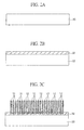
- the carbon nanotube sheet and method of manufacturing the carbon nanotube sheet according to a first embodiment will be explained with reference to FIGs. 1A to 3C .
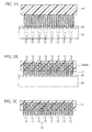
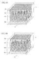
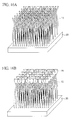
- FIGs. 1A and 1B are diagrammatic sectional views illustrating structures of a carbon nanotube sheet according to the present embodiment.
- FIGs. 2A-3C are sectional views illustrating a method of manufacturing the carbon nanotube sheet according to the present embodiment.
- FIG. 1A is a view illustrating a structure of a first example of the carbon nanotube sheet according to the present embodiment.
- FIG. 1B is a view illustrating a structure of a second example of the carbon nanotube sheet according to the present embodiment.
- the carbon nanotube sheet according to the present embodiment includes a plurality of carbon nanotubes 12 arranged, spaced from each other.
- a filling layer 14 of a thermoplastic resin material is formed in the gaps between the carbon nanotubes 12 and supports the carbon nanotubes 12.
- the carbon nanotube sheet 10 according to the present embodiment has a sheet structure, and the carbon nanotubes 12 are oriented in the film thickness-wise of the sheet, i.e., in the direction intersecting the surface of the sheet.
- the carbon nanotubes 12 may be single-walled carbon nanotubes or multi-walled carbon nanotubes.
- the density of the carbon nanotubes 12 is not especially limited but can be set preferably at not less than about 1 ⁇ 10 10 tubes/cm 2 from the view point of heat radiation and electric conduction.
- the length of the carbon nanotubes 12 may be determined by applications of the carbon nanotube sheet 10. It is not especially limited but can be set preferably at a value of about 5 - 500 ⁇ m.
- the length of the carbon nanotubes 12 preferably is not less than a length, which fills the concavities and convexities of at least the heat generation source and the heat radiation member.
- the carbon nanotube sheet 10 has at least one ends exposed.
- the carbon nanotube sheet illustrated in FIG. 1A has one ends of the carbon nanotubes 12 exposed.
- the carbon nanotube sheet illustrated in FIG. 1B has both ends of the carbon nanotubes 12 exposed.
- the carbon nanotube sheet 10 when the carbon nanotube sheet 10 is brought into contact with the heat radiator or the heat generator, the carbon nanotubes 12 are in direct contact with the heat radiator or the heat generator, whereby the thermal conductive efficiency can be drastically increased.
- the carbon nanotubes 12, which have also electric conductivity, have both ends exposed so as to be used as interconnection bodies passed through the sheet. That is, the carbon nanotube sheet 10 according to the present embodiment can be used not only as a thermal conductive sheet but also as a vertical interconnection sheet.
- the filling layer 14 is formed of a thermoplastic resin.
- the thermoplastic resin changes the phase reversibly between liquid and solid in accordance with temperatures.
- the thermoplastic resin is not specifically limited as far as it is solid at room temperature, and it changes to liquid by heating and, by cooling, returns to solid, exhibiting adhesiveness.
- thermoplastic resin is, e.g., the hot melt resins to be described below.
- polyamide-based hot melt resin "Micromelt 6239” (softening point temperature: 140 °C) from Henkel Japan Ltd., for example, may be applied.
- polyester-based hot melt resin “DH598B” (softening point temperature: 133 °C) from Nogawa Chemical Co., Ltd., for example, may be applied.
- polyurethane-based hot melt resin "DH722B” from Nogawa Chemical Co., Ltd., for example, may be applied.
- polyolefin-based hot melt resin "EP-90” (softening point temperature.
- 148 °C from Matsumura Oil Co., Ltd., for example, may be applied.
- ethylene copolymer hot melt resin "DA574B” (softening point temperature: 105 °C) from Nogawa Chemical Co., Ltd., for example, may be applied.
- SBR-based hot melt resin "M-6250" (softening point temperature: 125 °C) from Yokohama Rubber Co., Ltd., for example, may be applied.
- EVA-based hot melt resin "3747” (softening point temperature: 104 °C) from Sumitomo 3M Ltd., for example, may be applied.
- butyl rubber-based hot melt resin "M-6158” from Yokohama Rubber Co., Ltd., for example, may be applied.
- the thermoplastic resin forming the filling layer 14 can be selected based on the melting temperatures of the thermoplastic resins in accordance with uses of the carbon nanotube sheet 10. It is preferable that the lower limit value of the melting temperature of the thermoplastic resin is higher than the upper limit value of the heating temperature in operation. This is because when the thermoplastic resin melts in operation, there is a risk that the carbon nanotube sheet 10 may be deformed, the orientation of the carbon nanotubes 12 may be damaged, and resultantly the thermal conductivity may be lowered.
- the upper limit value of the melting temperature of the thermoplastic resin is lower than the lower limit value of the thermal resistance temperatures of the heat generator and the heat radiator.
- the carbon nanotube sheet 10 according to the present embodiment is preferably reflowed after brought into contact with the heat radiator and the heat generator. This is because when the melting temperature of the thermoplastic resin is higher than the thermal resistance temperature, the reflow is difficult without damaging the heat generator and/or the heat radiator. The reflow of the carbon nanotube sheet 10 will be detailed later.
- thermoplastic resins whose melting temperatures are about 125 °C ⁇ 250 °C are suitable in consideration that the upper limit of the heating temperature of the CPU in operation is 125 °C, and the heat resistance temperature of CPU electronic members is about 250 °C.
- thermoplastic resins whose melting temperature is about 600 °C ⁇ 900 °C are suitable in consideration that the heating temperature is about 500 °C ⁇ 800 °C although depending on parts.
- additives may be mixed dispersed as required.
- the additives for example, substances of high thermal conductivity and substances of high electric conductivity may be considered.
- Additives of high thermal conductivity are mixed dispersed in the filling layer 14 portion, whereby the thermal conductivity of the filling layer 14 portion can be improved, and the thermal conductivity of the carbon nanotube sheet 10 as a whole can be improved.
- an additive of high electric conductivity is mixed dispersed in the filling layer 14 portion, whereby the electric conductivity of the carbon nanotube sheet 10 as a whole can be improved.
- carbon nanotubes As material of high thermal conductivity, carbon nanotubes, metal material, aluminum nitride, silica, alumina, graphite, fullerene, etc. can be used. As materials of high electric conductivity, carbon nanotubes, metal materials, etc. can be used.
- the substrate 30 can be a semiconductor substrate, such as a silicon substrate or others, an insulating substrate, such as an alumina (sapphire) substrate, an MgO substrate, a glass substrate or others, a metal substrate or others.
- the substrate 30 can be such substrate with a thin film formed on.
- a silicon substrate with an about 300 nm-thickness silicon oxide film may be used.
- the substrate 30 is peeled off after the carbon nanotubes 12 have been grown. To this end, it is preferable that the substrate 30 is not deformed at a growth temperature of the carbon nanotubes 12. Also it is preferable that at least the surface of the substrate 30, which is in contact with the carbon nanotubes, is formed of a material which permits the surface to be easily peeled from the carbon nanotubes 12. It is also preferable that the substrate 30 is formed of a material which can be etched selectively with respective to the carbon nanotubes 12.
- an Fe (iron) film of a 2.5 nm-thickness for example, is formed by, e.g., sputtering method to form a catalyst metal film 32 of Fe ( FIG. 2B ) .
- the catalyst metal film 32 may not be formed essentially all over the substrate 30 and may be formed selectively over prescribed regions of the substrate 30 by, e.g., lift-off method.
- the catalyst metal can be, other than Fe, Co (cobalt), Ni (nickel), Au (gold), Ag (silver), Pt (platinum) or an alloy containing at least one of them.
- As the catalyst other than the metal film, metal particles prepared with the size controlled in advance with a DMA (Differential Mobility Analyzer) or others may be used. In this case, the metal species can be the same as those of the thin film.
- films of Mo molecular metals
- Ti titanium
- Hf hafnium
- Zr zirconium
- Nb niobium
- V vanadium
- TaN tantalum nitride
- TiSi x titanium silicide
- A1 aluminum
- Al 2 O 3 aluminum oxide
- TiO x titanium oxide
- Ta tantalum
- W tungsten
- Cu copper
- Au gold
- Pt platinum
- Pd palladium
- TiN titanium nitride
- an alloy containing at least one of them may be formed.
- the layer structure of Fe (2.5 5 nm)/A1 (10 nm), the layer structure of Co (2.6 nm)/TiN (5 nm), etc. can be used.
- the layer structure of, e.g., Co (average diameter: 3.8 nm)/TiN (5 nm), etc. can be used.
- the carbon nanotubes 12 are grown with the catalyst metal film 32 as the catalyst by, e.g., hot filament CVD method.
- the growth conditions for the carbon nanotubes 12 are, e.g., an acetylene-argon mixed gas (partial pressure ratio: 1:9) as the raw material gas, 1 kPa total gas pressure in the film forming chamber, 1000 °C hot filament temperature, 25 minute growth period of time.
- acetylene-argon mixed gas partial pressure ratio: 1:9
- 1 kPa total gas pressure in the film forming chamber 1000 °C hot filament temperature, 25 minute growth period of time.
- multi-walled carbon nanotubes of 3 - 6 layers (average: about 4 walls), 4 nm ⁇ 8 nm diameter (average: 6 nm) can be grown.
- the carbon nanotubes can be grown by another film forming process, such as thermal CVD method, remote plasma CVD method or others.
- the carbon nanotubes may be grown in a single-walled.
- the carbon raw material other than acetylene, hydrocarbons, such as methane, ethylene, etc. or alcohols, such as ethanol, methanol, etc. may be used.
- the length of the carbon nanotubes 12 is determined depending on an application of the carbon nanotube sheet 10 and is not specifically limited, but can be set preferably at a value of about 5 ⁇ m ⁇ 500 ⁇ m.
- the carbon nanotube sheet 10 as the thermal interface material to be formed between a heat generation source (e.g., semiconductor elements) and a heat radiation member (e.g., heat spreader)
- the carbon nanotubes 12 have preferably a length that fills at least the concavities and convexities in the surfaces of the heat generation source and the heat radiation member.
- a plurality of the carbon nanotubes 12 are formed, oriented in the normal direction of the substrate (vertically oriented) ( FIG. 2C ).
- the surface density of the carbon nanotubes 12 formed under the above growth conditions was about 1 ⁇ 10 11 tubes/cm 2 . This corresponds to that the carbon nanotubes 12 are formed in a region which is 10% of an area of the surface of the substrate 30.
- thermoplastic resin film 34 a thermoplastic resin processing in film (a thermoplastic resin film 34) is mounted ( FIG. 3A ).
- the film thickness of the thermoplastic resin film is set suitably depending on a length of the carbon nanotubes 12.
- the thermoplastic resin film 34 is formed preferably in a thickness that is about equal to a length of the carbon nanotubes 12, e.g., about 5 ⁇ m ⁇ 500 ⁇ m.
- the thermoplastic resin film 34 is formed preferably in a thickness that is little thin than a length of the carbon nanotubes 12, e.g., about 4 ⁇ m ⁇ 400 ⁇ m.
- the thermoplastic resin of the thermoplastic resin film 34 can be, e.g., hot melt resins described below.
- hot melt resins described below.
- polyamide-based hot melt resin "Micromelt 6239” (softening point temperature: 140 °C) from Henkel Japan Ltd., for example, may be applied.
- polyester-based hot melt resin “DH598B” (softening point temperature: 133 °C) from Nogawa Chemical Co., Ltd., for example, may be applied.
- polyurethane-based hot melt resin "DH722B” from Nogawa Chemical Co., Ltd., for example, may be applied.
- polyolefin-based hot melt resin "EP-90” (softening point temperature: 148 °C) from Matsumura Oil Co., Ltd., for example, may be applied.
- ethylene copolymer hot melt resin "DA574B” (softening point temperature: 105 °C) from Nogawa Chemical Co., Ltd., for example, may be applied.
- SBR-based hot melt resin "M-6250” (softening point temperature: 125 °C) from Yokohama Rubber Co., Ltd., for example, may be applied.
- EVA-based hot melt resin "3747” (softening point temperature: 104 °C) from Sumitomo 3M Ltd., for example, may be applied.
- butyl rubber-based hot melt resin "M-6158” from Yokohama Rubber Co., Ltd., for example, may be applied.
- thermoplastic resin film 34 of "Micromelt 6239” from Henkel Japan Ltd. processed in a 100 ⁇ m-thickness is used.
- "Micromelt 6239” is a hot melt resin whose melting temperature is 135 °C ⁇ 145 °C and whose viscosity when melted is 5.5 Pa.s ⁇ 8.5 Pa.s (225 °C).
- thermoplastic resin of the thermoplastic resin film 34 is melted and gradually penetrated into the gaps between the carbon nanotubes 12.
- the thermoplastic resin film 34 is thus penetrated to the extent that the thermoplastic resin film 34 does not arrive at the surface of the substrate 30.
- thermoplastic resin is process in film in advance, whereby a filling quantity can be controlled by a thickness of the film.
- a filling quantity can be controlled by a thickness of the film.
- thermoplastic resin film 34 The penetration of the thermoplastic resin film 34 is stopped to the extent that the thermoplastic resin film 34 does not arrive at the substrate 30, so that the carbon nanotube sheet 10 can be easily peeled from the substrate 30. In a case that the carbon nanotube sheet 10 can be easily peeled from the substrate 30, the thermoplastic resin film 34 maybe penetrated down to the substrate 30.
- the film thickness of the thermoplastic resin film 34 penetrating in the gaps between the carbon nanotubes 12 can be controlled by the heat processing period of time. For example, for the carbon nanotubes 12 of a 100 ⁇ m-length grown under the above-described conditions, the heat processing is made at 195 °C for 1 minute, whereby the thermoplastic resin film 34 can be penetrated to the extent that the thermoplastic resin film 34 does not arrive at the substrate 30.
- the heating period of time of the thermoplastic resin film 34 is suitably set corresponding to the length of the carbon nanotubes 12, a viscosity of the molten thermoplastic resin, a film thickness of the thermoplastic resin film 34, etc. so that the thermoplastic resin film 34 penetrates to the extent that the film 34 does not arrive at the substrate 30.
- thermoplastic resin is processed in film in advance, and the thermoplastic resin may be processed in pellets or rods.
- thermoplastic resin film 34 After the thermoplastic resin film 34 has been penetrated to a prescribed position, the thermoplastic resin film 34 is cooled to room temperature to set the thermoplastic resin film 34. Thus, the filling layer 14 formed of the thermoplastic resin of the thermoplastic resin film 34 and filled in the gaps between the carbon nanotubes 12 is formed.
- the carbon nanotubes 12 and the filling layer 14 are peeled from the substrate 30, and the carbon nanotube sheet according to the present embodiment is obtained ( FIG. 3C ).
- the filling layer 14 (the thermoplastic resin film 34) is formed, not arriving at the substrate 30 as described above, whereby the junction between the carbon nanotubes 12 and the substrate 30 is weak, and the carbon nanotubes 12 and the filling layer 14 can be easily peeled from the substrate 30.
- thermoplastic resin film 34 having the thickness smaller than the length of the carbon nanotubes 12 is used, and the thermoplastic resin film 34 is penetrated until the upper ends of the carbon nanotubes 12 are exposed.
- thermoplastic resin is used as the material of the filling layer supporting the carbon nanotubes, whereby the carbon nanotube sheet having the filling layer which can reflow and having small thermal contact resistance can be easily formed.
- the penetration quantity of the filling material can be easily controlled by the heat processing temperature and the heat processing period of time.
- the ends of the carbon nanotubes can be easily exposed.
- the sheet can be easily peeled from the substrate.
- the carbon nanotube sheet and the method of manufacturing the carbon nanotube sheet according to a second embodiment will be explained with reference to FIGs. 4 to 8 .
- the same members of the present embodiment as those of the carbon nanotube sheet and the method of manufacturing the carbon nanotube sheet according to the first embodiment illustrated in FIGs. 1A to 3C are represented by the same reference numbers not to repeat or to simplify their explanation.
- FIG. 4 is a diagrammatic sectional view illustrating a structure of a carbon nanotube sheet according to the present embodiment.
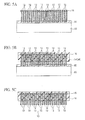
- FIGs. 5A-5C are sectional views illustrating a method of manufacturing the carbon nanotube sheet according to the present embodiment.
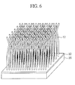
- FIGs. 6-8 are perspective views illustrating the method of manufacturing the carbon nanotube sheet according to the present embodiment.
- the carbon nanotube sheet 10 according to the present embodiment is the same as the carbon nanotube sheet 10 according to the fist embodiment illustrated in FIG. 1 except that in the present embodiment, a coating film 16 is formed on one ends of the carbon nanotubes 12.
- the material forming the coating film 16 is not specifically limited as far as the material has a higher thermal conductivity than the constituent material of the filling layer 14.
- electrically conductive materials e.g., metal, alloys, etc. can be used.
- the constituent material of the coating film 16 copper (Cu), nickel (Ni), gold (Au), etc., for example, can be used.
- the coating film 16 may not have essentially a single layer structure and may have multilayer structures of two layers or three or more layers, such as the layer structure of titanium (Ti) and gold (Au), etc.
- the thickness of the coating film 16 is not specifically limited as far as the coating film does not hinder the penetration of the thermoplastic resin film 34 in the manufacturing process.
- the film thickness of the coating film 16 is suitably determined depending on the permeability of the thermoplastic resin film 34, required characteristics of the carbon nanotube sheet 10, the constituent material of the coating film 16, etc.
- the coating film 16 of high thermal conductivity is provided, whereby the contact area of the carbon nanotube sheet 10 to a mounted body (a heat radiator, a heat generator) can be increased in comparison with the case where the coating film 16 is not provided. This decreases the thermal contact resistance between the carbon nanotubes 12 and the mounted body, and the thermal conductivity of the carbon nanotube sheet 10 can be increased. When the carbon nanotube sheet 10 is used as an electrically conductive sheet, the electric conductivity can be increased.
- the coating film 16 is formed on one ends of the carbon nanotubes 12 of the carbon nanotube sheet 10 illustrated in FIG. 1A . Also on the other ends of the carbon nanotubes 12, the coating film 16 may be formed. The coating film 16 may be formed on one ends or on both ends of the carbon nanotubes 12 of the carbon nanotube sheet illustrated in FIG. 1B .
- the carbon nanotubes 12 are grown over the substrate 30.
- the carbon nanotubes 12 are illustrated in simple cylindrical shapes so as to simplify the drawings, but the carbon nanotubes 12 are not always grown in perfect cylindrical shapes due to dispersions, etc. of the early growth.
- the carbon nanotubes 12 are oriented generally film-thickness-wise, but as illustrated in FIG. 6 , the upper end of the carbon nanotubes 12 may tilt from the normal of the substrate 30, and the length of the carbon nanotubes 12 may be disuniform.
- an about 300 nm-thickness Au (gold) film is deposited by, e.g., evaporation method to form the coating film 16 of Au ( FIG. 5A ).
- the coating film 16 may be formed by another film forming method (e.g., sputtering method or others) unless the method damages the carbon nanotubes 12.
- the material forming the coating film 16 is not specifically limited as far as the material has a higher thermal conductivity than a constituent material of the filling layer 14.
- electrically conductive materials e.g., metal, alloys, etc. can be used.
- the constituent material of the coating film 16 copper (Cu), nickel (Ni), gold (Au), etc., for example, can be used.
- the coating film 16 may not have essentially a single layer structure and may have multilayer structures of two layers or three or more layers, such as the layer structure of titanium (Ti) and gold (Au), etc.
- the coating film 16 is formed, covering the forward ends of the respective carbon nanotubes 12 in the early stage of the growth. As the grown film thickness increases, the coating film 16 formed on the forward ends of the respective carbon nanotubes 12 adjacent to each other is jointed. Thus, as exemplified in FIG. 8 , the coating film 16 is formed, bundling the forward ends of plural one of the carbon nanotubes 12. As the grown film thickness of the coating film 16 increases, the coating film 16 is completely jointed in the two-dimensional direction parallel with the surface of the sheet, and the coating film 16 becomes a unified film without gaps.
- the film thickness of the coating film 16 is suitably set corresponding to a diameter and a density of the carbon nanotubes 12 in consideration of the permeability of the thermoplastic resin film 34 for forming the filling layer 14, etc.
- the gap between the carbon nanotubes 12 adjacent to each other is about 50 nm.
- the coating film 16 is formed in a film thickness of at least above a half or more of the gap, i.e., the coating film is preferably formed in an about 25 nm or more film thickness.
- the coating film 16 becomes a perfect film without gaps, which lowers the permeability of the thermoplastic resin film 34.
- the upper limit of the film thickness of the coating film 16 is set in terms of the permeability of the thermoplastic resin film 34. In view of this, for the carbon nanotubes 12 of the above-conditions, the film thickness of the coating film 16 is set preferably at about 25 - 1000 nm.
- thermoplastic resin film 34 is penetrated in the gaps of the carbon nanotubes 12, and the filling layer 14 is formed ( FIG. 5B ).
- the coating film 16 may not be essentially formed in a film thickness sufficient to joint the carbon nanotubes 12 adjacent to each other but has the effect of bundling plural ones of the carbon nanotubes 12 (see FIG. 8 ).
- the thermoplastic resin film 34 is penetrated into the gaps between the carbon nanotubes 12, the carbon nanotubes 12 are hindered from separating from each other. Also, the heat can be caused to conduct transversely.
- the carbon nanotubes 12, the coating film 16 and the filling layer 14 are peeled from the substrate 30, and the carbon nanotube sheet according to the present embodiment is obtained ( FIG. 5C ).
- the same coating film (not illustrated) as the coating film 16 is formed on the ends of the carbon nanotubes 12 from which the substrate 30 has been peeled.
- thermoplastic resin is used as the material of the filling layer supporting the carbon nanotubes, whereby the carbon nanotube sheet having the filling layer which can reflow and having small thermal contact resistance can be easily formed.
- the penetration quantity of the filling material can be easily controlled by the heat processing temperature and the heat processing period of time.
- the ends of the carbon nanotubes can be easily exposed.
- the sheet can be easily peeled from the substrate.
- the coating film of a material whose thermal conductivity is higher than the filling layer is formed on the ends of the carbon nanotubes, whereby the thermal contact resistance to a mounted body can be drastically lowered.
- the carbon nanotube sheet and the method of manufacturing the carbon nanotube sheet according to a third embodiment will be explained with reference to FIGs. 9 to 14 .
- the same members of the present embodiment as those of the carbon nanotube sheet and the method of manufacturing the carbon nanotube sheet according to the first and the second embodiments illustrated in FIGs. 1A to 8 are represented by the same reference numbers not to repeat or to simplify their explanation.
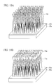
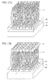
- FIGs. 9A and 9B are perspective views illustrating structures of a carbon nanotube sheet according to the present embodiment.
- FIGs. 10A-13 are perspective views illustrating a method of manufacturing the carbon nanotube sheet according to the present embodiment.
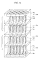
- FIG. 14 is a perspective view illustrating a method of manufacturing the carbon nanotube sheet according to another example of the present embodiment.
- FIG. 9A illustrates a first example of the carbon nanotube sheet according to the present embodiment
- FIG. 9B illustrates a second example of the carbon nanotube sheet according to the present embodiment.
- the carbon nanotube sheet 10 according to the present embodiment is the same as the carbon nanotube sheet according to the first and the second embodiments in that, as illustrated in FIG. 9A and FIG. 9B , a plurality of carbon nanotubes 12 are spaced from each other, and the filling layer 14 of a thermoplastic resin is buried in the gaps.
- the carbon nanotube sheet 10 includes a plurality of carbon nanotubes 12a and a plurality of carbon nanotubes 12b.
- the plural carbon nanotubes 12a have a coating film 16a on the ends thereof which are on the side of one surface of the carbon nanotube sheet 10 (upper surface as viewed in the drawing).
- the plural carbon nanotubes 12b have a coating film 16b on the ends thereof which are on the side of the other surface of the carbon nanotube sheet 10 (lower surface as viewed in the drawing).
- the carbon nanotube sheet 10 of the first example illustrated in FIG. 9A and the carbon nanotube sheet 10 of the second example illustrated in FIG. 9B are different from each other in the thickness of the coating films 16a, 16b. That is, in the carbon nanotube sheet 10 of the first example illustrated in FIG. 9A , as has been explained with reference to FIG. 7 , the coating films 16a, 16b are formed, respectively covering the ends of the carbon nanotubes 12a and the ends of the carbon nanotubes 12b. In the carbon nanotube sheet 10 of the second example illustrated in FIG. 9B , as has been explained with reference to FIG. 8 , the coating films 16a, 16b are respectively formed, bundling the ends of plural ones of the carbon nanotubes 12a and the ends of plural ones of the carbon nanotubes 12b.
- the constituent materials of the filling material 14 and the coating film 16 are the same as those of the carbon nanotube sheet according to the first or the second embodiment.
- the method of manufacturing the carbon nanotube sheet according to the present embodiment will be explained with reference to FIGs. 10A to 13 .
- the method of manufacturing the carbon nanotube sheet of the second example illustrated in FIG. 9B will be explained here, but the method of manufacturing the carbon nanotube sheet of the first example illustrated in FIG. 9A is the same as the method of manufacturing the carbon nanotube sheet of the second example except that the thickness of the coating film 16 is different.
- a plurality of carbon nanotubes 12a are grown over the substrate 30a ( FIG. 10A ).
- the coating film 16a is formed on the carbon nanotubes 12a ( FIG. 10B ).
- thermoplastic resin film 34 is penetrated between the carbon nanotubes 12a to form the filling layer 14a of the thermoplastic resin material ( FIG. 11A ).
- the thermoplastic resin film 34 (the filling layer 14) is penetrated down to the substrate 30, but, as in the first and the second embodiments, it may be penetrated to the extent that the thermoplastic resin film 34 does not arrive at the substrate 30a.
- the carbon nanotube sheet 10a is the same as the carbon nanotube sheet 10 according to the second embodiment.
- the carbon nanotube sheet 10b including the carbon nanotubes 12b with the coating film 16b formed on buried in the filling layer 14b is prepared.
- the carbon nanotube sheet 10a and the carbon nanotube sheet 10b are laid on each other with the surfaces thereof where the coating films 16a, 16b are not formed ( FIG. 12 ).
- the layer body of the carbon nanotube sheet 10a and the carbon nanotube sheet 10b is heated under load.
- the layer body is heated at 195 °C under a 10 N/cm 2 pressure.
- the filling layer 14a, 14b are melted and liquefied to be unified, the carbon nanotubes 12a are inserted in the gaps between the carbon nanotubes 12b, and the carbon nanotubes 12b are inserted in the gaps between the carbon nanotubes 12a.
- the layer body is cooled to room temperature to set the filling layers 14a, 14b (hereinafter called the filling layer 14).
- the carbon nanotube sheet 10 having the carbon nanotubes 12a with the coating film 16a formed on, and the carbon nanotubes 12b with the coating film 16b formed on buried in the filling layer 14 is formed ( FIG. 13 ).
- the surface density of the carbon nanotubes 12a, 12b varies depending on growth conditions of the carbon nanotubes. For example, even when the carbon nanotubes 12 are formed in a surface density of about 1 ⁇ 10 12 cm -2 , the surface density of the carbon nanotubes 12 can be doubled by the method of manufacturing the carbon nanotube sheet according to the present embodiment. Thus, the thermal conductivity and the heat radiation efficiency of the carbon nanotube sheet can be drastically improved.
- More sheets of the carbon nanotube sheet are laid on, whereby the surface density of the carbon nanotubes can be further increased.
- a carbon nanotube sheet 10c with the carbon nanotubes 12c buried in the filling layer 14c, and the carbon nanotube sheet 10d with the carbon nanotubes 12d buried in the filling layer 14d may be sandwiched.
- the surface density of the carbon nanotubes can be made four times.
- the number of the carbon nanotube sheets to be laid on can be suitably set corresponding to a required thermal conductivity and heat radiation efficiency.
- the carbon nanotube sheet 10a and the carbon nanotube sheet 10c, and the carbon nanotube sheet 10b and the carbon nanotube sheet 10d are respectively unified, and then the two unified sheets can be unified. Otherwise, it is possible to unify the carbon nanotube sheet 10a and the carbon nanotube sheet 10c, then unify the carbon nanotube sheet 10d therewith, and furthermore, unify the carbon nanotube sheet 10b therewith.
- the carbon nanotube sheets 10c, 10d may not have the coating film on the ends so as to facilitate the insertion of the carbon nanotubes 12c, 12d in the gaps between the carbon nanotubes of the other sheets.
- the carbon nanotube sheets 10c, 10d can be manufactured by the same procedures as those of, e.g., the method of manufacturing the carbon nanotube sheet according to the first embodiment.
- a plurality of carbon nanotube sheet having the filling layer supporting the carbon nanotubes formed of a thermoplastic resin are laid on and are unified by thermal processing, whereby the surface density of the carbon nanotubes can be drastically improved.
- the thermal conductivity of the sheet can be drastically improved.
- the carbon nanotube sheet and the method of manufacturing the carbon nanotube sheet according to a fourth embodiment will be explained with reference to FIG. 15A to FIG. 19 .
- the same members of the present embodiment as those of the carbon nanotube sheet and the method of manufacturing the carbon nanotube sheet according to the first to the third embodiments illustrated in FIGs. 1A to 14 are represented by the same reference numbers not to repeat or to simplify their explanation.
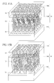
- FIGs. 15A and 15B are perspective views illustrating structures of a carbon nanotube sheet according to the present embodiment.
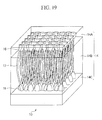
- FIGs. 16A-16B , 17A-17B , 18A-18B and 19 are perspective views illustrating a method of manufacturing the carbon nanotube sheet according to the present embodiment.
- FIG. 15A illustrates a first example of the carbon nanotube sheet according to the present embodiment
- FIG. 15B illustrates a second example of the carbon nanotube sheet according to the present embodiment.
- the carbon nanotube sheet 10 according to the present embodiment is the same as the carbon nanotube sheet according to the first to the third embodiments in that a plurality of carbon nanotubes 12 are spaced from each other, and the filling layer 14 of a thermoplastic resin is buried in the gaps.
- the filling layer 14 is formed of the layer body of the filling layers 14A, 14B and 14C.
- the coating films 16 are formed on both ends of the carbon nanotubes 12.
- the filling layers 14A, 14C are formed of the same thermoplastic resin as the thermoplastic resin forming the filling layer 14 of the carbon nanotube sheet according to the first to the third embodiments.
- the constituent material of the coating film 16 is the same as the coating film 16 of the carbon nanotube sheet according to the first to the third embodiments.
- the material of the filling layer 14B is not especially limited as long as the material exhibits the liquid properties when burying the carbon nanotubes 12.
- the organic filling material acryl resin, epoxy resin, silicone resin, polyimide resin, etc.
- the inorganic filling material compositions for the spin on insulating film, e.g., SOG (Spin On Glass) can be used.
- Metal materials such as indium, solder, metal paste (e.g., silver paste), etc. can be also used.
- Electrically conductive polymers e.g., polyaniline, polyolefine, etc. can be also used.
- additives may be mixed dispersed as required.
- the additives for example, substances of high thermal conductivity and substances of high electric conductivity may be considered.
- Additives of high thermal conductivity are mixed dispersed in the filling layer 14B portion, whereby the thermal conductivity of the filling layer 14B portion can be improved, and the thermal conductivity of the carbon nanotube sheet 10 as a whole can be improved.
- an additive of high electric conductivity is mixed dispersed in the filling layer 14B portion, whereby the electric conductivity of the carbon nanotube sheet 10 as a whole can be improved.
- carbon nanotubes As material of high thermal conductivity, carbon nanotubes, metal material, aluminum nitride, silica, alumina, graphite, fullerene, etc. can be used. As materials of high electric conductivity, carbon nanotubes, metal materials, etc. can be used.
- the filling layer 14 is formed of a material of high thermal conductivity, whereby the thermal conductivity of the sheet as a whole can be improved.
- the thermal conductivity of the thermoplastic resin is ordinarily not more than 0.1 [W/m-K], and the whole filling layer 14 formed of the thermoplastic resin does not substantially contribute to the heat conduction.
- the filling layer 14B is formed of a material of some high thermal conductivity, e.g., a electrically conductive polymer in place of the thermoplastic resin, and the filling layers 14A, 14C are formed of the thermoplastic resin in consideration of the adhesion and the interface heat resistance in operation, whereby the thermal conductivity of the sheet as a whole can be improved.
- the carbon nanotube sheet of the first example illustrated in FIG. 15A and the carbon nanotube sheet 10 of the second example illustrated in FIG. 15B are different from each other in the thickness of the coating films 16. That is, in the carbon nanotube sheet 10 of the first example illustrated in FIG. 15A , as has been explained with reference to FIG. 7 , the coating film 16 is formed, covering the forward ends of the respective carbon nanotubes 12. In the carbon nanotube sheet 10 of the second example illustrated in FIG. 15B , as has been explained with reference to FIG. 8 , the coating film 16 is formed, bundling the forward ends of plural ones of the carbon nanotubes 12.
- the method of manufacturing the carbon nanotube sheet according to the present embodiment will be explained with reference to FIGs. 16A to 19 .
- the method of manufacturing the carbon nanotube sheet of the second example illustrated in FIG. 15B will be explained here, but the method of manufacturing the carbon nanotube sheet of the first example illustrated in FIG. 15A is the same as the method of manufacturing the carbon nanotube sheet of the second example except that the thickness of the coating film 16 is different.
- a plurality of carbon nanotubes 12 are formed over the substrate 30 ( FIG. 16A ).
- the coating film 16 is formed on one ends of the carbon nanotubes 12 ( FIG. 16B ).
- a photoresist film of a 6 ⁇ m-thickness for example, is applied to the substrate 40 by, e.g., spin coating method.
- the substrate 40 is not especially limited but can be, e.g., a sapphire substrate or others.
- films of other materials which are etching selective to the filling layer 14B can be formed.
- the substrate 30 is mounted with the surfaces of the carbon nanotubes 12 the coating film 16 is formed on opposed thereto, and the photoresist film 42 is set.
- the ends of the carbon nanotubes 12 covered by the coating film 16 are covered by the photoresist film 42.
- the substrate 30 is peeled from the carbon nanotubes 12.
- the carbon nanotubes 12 with the coating film 16 formed on are transferred to the substrate 40 ( FIG. 17A ).
- the coating film 16 is formed on the other ends of the carbon nanotubes 12 ( FIG. 17B ).
- a filling material to be the filling layer 14B is applied.
- the viscosity of the coating solution and the rotation number of the spin coater are suitably set so that the thickness of the filling material on the coating film 16 becomes not more than tens nm.
- the filling material to be the filling layer 14B is not especially limited as far as the filling material can be set thereafter.
- organic filling materials acryl resin, epoxy resin, silicone resin, polyimide resin, etc. can be used.
- inorganic filling materials compositions for forming spin on insulating film, such as SOG (Spin On Glass), etc., can be used.
- metal materials such as indium, solder, metal paste (e.g., silver paste), etc.
- Electrically conductive polymers e.g., polyaniline, polyolefine, etc. can be used.
- a silicone-based resin is used here.
- the filling material is set by thermal processing, UV radiation or others, and the filling layer 14B is formed ( FIG. 18A ).
- the photoresist film 42 is selectively removed by, e.g., an organic solvent to peel from the substrate 40 the carbon nanotubes 12 buried in the filling layer 14B and having the coating film 16 formed on the ends ( FIG. 18B ). At this time, one ends of the carbon nanotubes 12 which have been covered by the photoresist film 42 are not covered by the filling layer 14B.
- the filling layers 14A, 14C of a thermoplastic resin material are formed on both surfaces of the filling layer 14B.
- the carbon nanotube sheet 10 according to the present embodiment having the carbon nanotubes 12 with the coating films 16 formed on buried in the filling layer 14 of the layer body of the filling layers 14A, 14B, 14C is formed ( FIG. 19 ).
- thermoplastic resin layer is provided on the surface of the filling layer supporting the carbon nanotubes, whereby the carbon nanotube sheet of small thermal contact resistance to a mounted body can be manufactured.
- the electronic device and the method of manufacturing the electronic device according to a fifth embodiment will be explained with reference to FIGs. 20 to 22B .
- the same members of the present embodiment as those of the carbon nanotube sheet and the method of manufacturing the carbon nanotube sheet according to the first to the fourth embodiments illustrated in FIGs. 1A to 19 are represented by the same reference numbers not to repeat or to simplify their explanation.
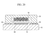
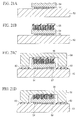
- FIG. 20 is a diagrammatic sectional view illustrating the structure of the electronic device according to the present embodiment.
- FIGs. 21A-21D are sectional views illustrating the method of manufacturing the electronic device according to the present embodiment.
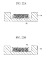
- FIGs. 22A and 22B are diagrammatic sectional views illustrating the structures of the electronic parts according to the fifth embodiment.
- circuit substrate 50 such as a multi-level interconnection substrate, etc.
- semiconductor element 54 e.g., CPU, etc. is mounted.
- the semiconductor element 54 is electrically connected to the circuit substrate 50 via projected electrodes 52, such as solder bumps, etc.
- a heat spreader 58 for dispersing the heat from the semiconductor element 54 is formed, covering the semiconductor element 54.
- the carbon nanotube sheet 56 according to any one of the first to the fourth embodiments is formed.
- the heat spreader 58 is adhered to the circuit substrate 50 with, e.g., an organic sealant 60.
- the carbon nanotube sheet according to the first to the fourth embodiments is provided between the semiconductor element 54 and the heat spreader 58, i.e., the heat generator and the heat radiator.
- the carbon nanotube sheet according to the first to the fourth embodiments has the carbon nanotubes 12 oriented in the direction of thickness of the sheet, and the thermal conductivity vertical to the plane is very high.
- the carbon nanotube sheet according to the second to the fourth embodiment has the coating film 16 on one ends or both ends of the carbon nanotubes 12, whereby the thermal contact resistance can be drastically decreased.
- the described carbon nanotube sheet is used as the heat conductive sheet formed between the semiconductor element 54 and the heat spreader 58, whereby the heat generated from the semiconductor element 54 can be effectively vertically conducted to the heat spreader 58, and the heat radiation efficiency can be increased.
- the reliability of the electronic device can be improved.
- the carbon nanotube sheet 56 has at least the surface of the filling layer supporting the carbon nanotubes 12 formed a thermoplastic resin material.
- the adhesion of the carbon nanotube sheet 56 to the semiconductor element 54 and the heat spreader 58 can be improved, and the thermal conductivity of the carbon nanotube sheet 56 can be improved.
- the semiconductor element 54 is mounted via the projected electrodes 52 ( FIG. 21A ).
- the concavities and convexities of the surfaces of the semiconductor element 54 and the heat spreader 58 opposed to each other are emphasized.
- the carbon nanotube sheet 56 described in any one of the first to the fourth embodiments is mounted ( FIG. 21B ).
- the carbon nanotube sheet according to the first embodiment is used, but the carbon nanotube sheet according to the second to the fourth embodiments may be used.
- the organic sealant 60 for securing the heat spreader 58 is applied, and the heat spreader 58 is mounted on the semiconductor element 54 with the carbon nanotube sheet 56 mounted on ( FIG. 21C ).
- heat processing is made to reflow the carbon nanotube sheet 56.
- the heat processing is made, e.g., at 195 °C and for 10 minutes under a 0.25 MPa load.
- This heat processing melts and liquefies the thermoplastic resin forming the carbon nanotubes sheet 56 to deform the carbon nanotube sheet 56 along the concavities and convexities in the surfaces of the semiconductor element and the heat spreader 58.
- the carbon nanotubes 12 in the carbon nanotube sheet 54 is less restricted by the filling layer 14, and the ends of the carbon nanotubes 12 come into direct contact with the semiconductor element 54 and the heat spreader 58.
- the carbon nanotubes 12, the material of which is flexible and soft can flex in accordance with the concavities and convexities of the semiconductor element 54 and the heat spreader 58.
- more of the carbon nanotubes 12 are in direct contact with the semiconductor element 54 and the heat spreader 58, whereby the thermal contact resistance between the carbon nanotube sheet 56, and the semiconductor element 54 and the heat spreader 58 can be drastically decreased.
- the load at this time may be in the load range which the carbon nanotube sheet 56 is deformed along the concavities and convexities present in the surfaces of the semiconductor element 54 and the heat spreader 58 to be into sufficient contact therewith.
- the temperature and the period of time of the heat processing may be selected in the range which the thermoplastic resin present in the interface between the semiconductor element 54 and the heat spreader 58 is melted and flows to form the surface state that the ends of the carbon nanotubes 12 are in direct contact with the semiconductor element 54 and the heat spreader 58.
- the electronic device is cooled to room temperature to set the thermoplastic resin of the filling layer 14 while securing the heat spreader 58 to the circuit substrate 50 with the organic sealant 60.
- the thermoplastic resin exhibit adhesiveness and can securely adhere the semiconductor element 54 and the heat spreader 58 to each other by the carbon nanotube sheet 56.
- the low thermal contact resistance between the carbon nanotube sheet 56, and the semiconductor element 54 and the heat spreader 58 can be retained.
- the carbon nanotube sheet having the filling layer 14 formed of a material other than a thermoplastic resin cannot exhibit adhesiveness to the once set filling layer 14, and the carbon nanotube sheet, and the semiconductor element 54 and the heat spreader are adhered only by press contact. Even when the semiconductor element 54 and the heat spreader 58 are press-contacted, the ends of the carbon nanotubes 12 cannot directly contact with the semiconductor element 54 and the heat spreader 58. It will be an idea of exposing the ends of the carbon nanotubes 12 in advance, but it is difficult to etch the filling layer 14 alone with the selectivity between the carbon nanotubes 12 and the filling layer 14 being sufficiently ensured. Thus, the thermal contact resistance between the semiconductor element 54 and the heat spreader 58 cannot be sufficiently decreased.
- the carbon nanotube sheet 56 and the heat spreader 58 are prepared as independent electronic parts, but the carbon nanotube sheet 56 may be formed in advance in the inside surface of the heat spreader 58.
- the surface of the carbon nanotube sheet 56 with the filling layer 14 formed on can be adhered to the inside surface of the heat spreader 58.
- the surface of the carbon nanotube sheet 56 where the carbon nanotubes 12 are exposed can be adhered to the inside surface of the heat spreader 58.
- the electronic parts exemplified in FIG. 22A can be manufactured by manufacturing the carbon nanotube sheet 56 the heat spreader 58 independently, then mounting the carbon nanotube sheet 56 on the inside surface of the heat spreader 58, making heat processing with a load being applied as required to adhere the carbon nanotube sheet 56.
- the electronic parts of FIG. 22A is applicable, as the carbon nanotube sheet 56, to not only the carbon nanotube sheet according to the first or the second embodiment but also to the carbon nanotube sheet according to the third and the fourth embodiments.
- the electronic parts of FIG. 22B can be manufactured in the same way as in, e.g., the method of manufacturing the carbon nanotube sheet according to the first or the second embodiment by using the heat spreader 58 as the substrate 30.
- the carbon nanotube sheet according to the first to the fourth embodiment is disposed between the semiconductor element and the heat spreader, whereby the thermal conductivity between them can be drastically improved.
- the heat radiation efficiency of the heat generated by the semiconductor element can be improved, and the reliability of the electronic device can be improved.
- the electronic device and the method of manufacturing the electronic device according to a sixth embodiment will be explained with reference to FIGs. 23 to 24B .
- the carbon nanotube sheet and the method of manufacturing the carbon nanotube sheet according to the first to the fourth embodiment illustrated in FIGs. 1 to 19 and the electronic device and the method of manufacturing the electronic device according to the fifth embodiment illustrated in FIGs. 20 to 22B are represented by the same reference numbers not to repeat or to simplify their explanation.
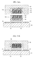
- FIG. 23 is a diagrammatic sectional view illustrating the structure of the electronic device according to the present embodiment.
- FIGs. 24A-24B are sectional views illustrating the method of manufacturing the electronic device according to the present embodiment.
- the electronic device according to the present embodiment corresponds to the electronic device according to the fifth embodiment having the carbon nanotube sheet 56 according to the third embodiment disposed between the semiconductor element 54 and the heat spreader 58.
- the carbon nanotube sheet 10a having the carbon nanotubes 12a with the coating film 16a formed on buried in the filling layer 14a, and the carbon nanotube sheet 10b having the carbon nanotubes 12b with the coating film 16b formed on buried in the filling layer 14b are prepared.
- the semiconductor element 54 is mounted on the circuit substrate 50 with the projected electrodes 52.
- the carbon nanotube sheet 10b is adhered to the upper surface of the semiconductor element 54.
- the carbon nanotube sheet 10a is adhered to the inside surface of the heat spreader 58.
- the carbon nanotube sheets 10a, 10b can be adhered to the semiconductor element 54 and the heat spreader 58 by mounting the carbon nanotube sheets 10a, 10b on the semiconductor element 54 and the heat spreader 58, and then heat processing under load as required.
- the organic sealant 60 for securing the heat spreader 58 is applied to the circuit substrate 30, and then the heat spreader 58 with the carbon nanotube sheet 10a adhered is mounted over the semiconductor element 54 with the carbon nanotube sheet 10b adhered to ( FIG. 24A ).
- the carbon nanotube sheet 56 according to the third embodiment is formed between the semiconductor element 54 and the heat spreader 58.
- the carbon nanotube sheet 56 is formed, and simultaneously therewith the carbon nanotube sheet 56 is deformed in accordance with the concavities and convexities in the surface of the semiconductor element 54 and the heat spreader 58. Also, the carbon nanotubes 12a, 12b in the carbon nanotube sheet 54 are less restricted by the filling layer 14 and have the ends in direct contact with the semiconductor element 54 and the heat spreader 58 (this is the same with the case where the coating films 16a, 16b are formed). Thus, the thermal contact resistance between the carbon nanotube sheet 56, and the semiconductor element 54 and the heat spreader 58 can be drastically decreased.
- the load at this time may be in a load range that the carbon nanotube sheets 10a, 10b are unified, and the carbon nanotube sheet 56 is deformed along the concavities and convexities present in the surface of the semiconductor element 54 and the heat spreader 58 to be brought into sufficient contact.
- the temperature and the period of time of the heat processing may be selected in the range that the thermoplastic resin present in the interface between the semiconductor element 54 and the heat spreader 58 is melted an flow to bring the ends of the carbon nanotubes 12 into direct contact with the semiconductor element 54 and the heat spreader 58.
- the electronic device is cooled to room temperature to set the thermoplastic resin of the filling layer 14 and secure the heat spreader 58 to the circuit substrate 50 by the organic sealant 60.
- the thermoplastic resin exhibits adhesiveness to thereby securely adhere the semiconductor element 54 and the heat spreader 58 to each other by the carbon nanotube sheet 56.
- the carbon nanotube sheet according to the third embodiment is disposed between the semiconductor element and the heat spreader, whereby the thermal conductivity between them can be drastically improved.
- the heat radiation efficiency of the heat generated by the semiconductor element can be increased, and the reliability of the electronic device can be improved.
- the electronic device according to a seventh embodiment will be explained with reference to FIG. 25 .
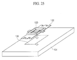
- FIG. 25 is a perspective view illustrating the structure of the electronic device according to the present embodiment.
- the electronic device using the carbon nanotube sheet according to the first to the fourth embodiment as the heat conductive sheet which functions also as the electrically conductive sheet will be explained.
- the HPA (High Power Amplifier) 70 used in, e.g., the radio communication stations is built in a package 72 and is jointed to the heat sink 74 at back surface of the package 72.
- the heat generated by the HPA 70 is radiated to the heat sink 74 through the back surface of the package 72.
- the package 72 also used as the electric ground (ground surface) and must be electrically connected to the heat sink 74.
- an electrically and thermally good conductor is preferably used for the joint between the package 72 and the heat sink 74.
- the carbon nanotube sheet according to the first to the fourth embodiments permits the carbon nanotubes 12 or the carbon nanotubes 12 with the coating film 16 formed on to be directly contacted to a heat generator or a heat radiator. That is, the carbon nanotube sheet according to the first to the fourth embodiment can be used not only as a heat radiation sheet, but also as an electrically conductive sheet.
- the carbon nanotube sheet 76 according to any one of the first to the fourth embodiments is used at the joint between the package 72 and the heat sink 74, whereby the package 72 and the heat sink 74 can be electrically connected to each other.
- the heat generated by the HPS 70 can be efficiently conducted to the heat sink 74, whereby the heat radiation efficiency can be increased.
- the reliability of the electronic deice can be improved.
- the electronic device according to the present embodiment can be manufactured in the same way as in, e.g., the method of manufacturing the electronic device according to the fifth or the sixth embodiment.
- the carbon nanotube sheet according to the first to the fourth embodiments is disposed between the package of the HPA and heat sink, whereby the thermal conductivity between them can be drastically improved.
- the heat radiation efficiency of the heat generated by the HPA can be increased.
- the reliability of the electronic device can be increased.
- the HPA and the heat sink as the ground can be electrically connected to each other.
- the sheet structure using the linear structure of carbon atoms is exemplified by carbon nanotube sheet using carbon nanotubes, but the sheet structure using the linear structure of carbon atoms is not limited to this.
- the linear structure of carbon atoms other than carbon nanotubes, carbon nanowires, carbon rods and carbon fibers are listed. These linear structures are the same as the carbon nanotubes except that they are different from the carbon nanotubes in size. The embodiments are applicable to the sheet structures using these linear structures.
- the uses of the carbon nanotube sheet are not limited to those described in the embodiments described above.
- the described carbon nanotube sheet is applicable, as the heat conductive sheet, to, e.g., the heat radiation sheet of CPUs, high power amplifiers of radio communication stations, high power amplifiers for radio communication terminals, high power switches for electric motors, servers, personal computers, etc.
- the carbon nanotube sheet can be applicable to vertical interconnection sheets and various applications using the vertical interconnection sheets.
Landscapes
- Engineering & Computer Science (AREA)
- Physics & Mathematics (AREA)
- Thermal Sciences (AREA)
- Mechanical Engineering (AREA)
- General Engineering & Computer Science (AREA)
- Cooling Or The Like Of Semiconductors Or Solid State Devices (AREA)
- Carbon And Carbon Compounds (AREA)
- Cooling Or The Like Of Electrical Apparatus (AREA)
- Laminated Bodies (AREA)
Applications Claiming Priority (1)
| Application Number | Priority Date | Filing Date | Title |
|---|---|---|---|
| JP2008292320A JP5239768B2 (ja) | 2008-11-14 | 2008-11-14 | 放熱材料並びに電子機器及びその製造方法 |
Publications (3)
| Publication Number | Publication Date |
|---|---|
| EP2187440A2 true EP2187440A2 (fr) | 2010-05-19 |
| EP2187440A3 EP2187440A3 (fr) | 2010-10-27 |
| EP2187440B1 EP2187440B1 (fr) | 2017-02-15 |
Family
ID=41559683
Family Applications (1)
| Application Number | Title | Priority Date | Filing Date |
|---|---|---|---|
| EP09173510.0A Active EP2187440B1 (fr) | 2008-11-14 | 2009-10-20 | Matériau à radiation de chaleur, dispositif électronique et procédé de fabrication du dispositif électronique |
Country Status (6)
| Country | Link |
|---|---|
| US (2) | US8194407B2 (fr) |
| EP (1) | EP2187440B1 (fr) |
| JP (1) | JP5239768B2 (fr) |
| KR (1) | KR101217204B1 (fr) |
| CN (1) | CN101740529B (fr) |
| TW (1) | TWI477593B (fr) |
Cited By (5)
| Publication number | Priority date | Publication date | Assignee | Title |
|---|---|---|---|---|
| WO2011017136A1 (fr) * | 2009-08-04 | 2011-02-10 | Raytheon Company | Structure dinterface thermique de nanotube |
| WO2013044094A3 (fr) * | 2011-09-21 | 2013-11-07 | Georgia Tech Research Corporation | Procédé de réduction de la résistance thermique d'ensembles ou de feuilles de nanotubes de carbone |
| JP2014003144A (ja) * | 2012-06-18 | 2014-01-09 | Fujitsu Ltd | 電子機器の製造方法及び電子機器 |
| EP2546871A4 (fr) * | 2010-03-12 | 2018-01-03 | Fujitsu Limited | Structure de dissipation de chaleur, et procédé de fabrication de celle-ci |
| WO2020094340A1 (fr) * | 2018-11-05 | 2020-05-14 | Robert Bosch Gmbh | Dissipateur thermique comprenant des fibres à base de nanostructures de carbone |
Families Citing this family (54)
| Publication number | Priority date | Publication date | Assignee | Title |
|---|---|---|---|---|
| JP5356972B2 (ja) * | 2009-10-20 | 2013-12-04 | 新光電気工業株式会社 | 放熱用部品及びその製造方法、半導体パッケージ |
| IT1401734B1 (it) * | 2010-06-29 | 2013-08-02 | St Microelectronics Srl | Dispositivo elettronico comprendente uno strato di interfaccia di connessione basato su nanotubi, e procedimento di fabbricazione |
| JP5790023B2 (ja) * | 2011-02-25 | 2015-10-07 | 富士通株式会社 | 電子部品の製造方法 |
| US20120228000A1 (en) * | 2011-03-10 | 2012-09-13 | Quan Geo Enterprise Co., Ltd. | Conductive adhesive having multiple curved lead wires therein |
| JP5842349B2 (ja) * | 2011-03-18 | 2016-01-13 | 富士通株式会社 | シート状構造体、シート状構造体の製造方法、電子機器及び電子機器の製造方法 |
| EP2698591A4 (fr) * | 2011-04-12 | 2014-11-05 | Ngk Insulators Ltd | Commutateur d'écoulement de chaleur |
| JP5673325B2 (ja) * | 2011-04-20 | 2015-02-18 | 富士通株式会社 | カーボンナノチューブの形成方法及び熱拡散装置 |
| US9459056B2 (en) * | 2011-09-02 | 2016-10-04 | Gabe Cherian | SPRDR—heat spreader—tailorable, flexible, passive |
| JP6132768B2 (ja) * | 2011-09-26 | 2017-05-24 | 富士通株式会社 | 放熱材料及びその製造方法 |
| JP2013115094A (ja) * | 2011-11-25 | 2013-06-10 | Fujitsu Ltd | 放熱材料及びその製造方法 |
| JP5580282B2 (ja) * | 2011-12-09 | 2014-08-27 | 本田技研工業株式会社 | バッテリの冷却装置 |
| JP6015009B2 (ja) * | 2012-01-25 | 2016-10-26 | 富士通株式会社 | 電子装置及びその製造方法 |
| TWI543702B (zh) * | 2012-02-08 | 2016-07-21 | 鴻準精密工業股份有限公司 | 散熱裝置 |
| JP6065410B2 (ja) * | 2012-05-16 | 2017-01-25 | 富士通株式会社 | シート状構造体、シート状構造体の製造方法、電子機器及び電子機器の製造方法 |
| KR101374818B1 (ko) * | 2012-05-22 | 2014-03-17 | 롯데케미칼 주식회사 | 열가소성 수지 조성물 |
| JP2014033104A (ja) * | 2012-08-03 | 2014-02-20 | Shinko Electric Ind Co Ltd | 放熱部品及びその製造方法 |
| FR2995877B1 (fr) * | 2012-09-21 | 2014-10-24 | Thales Sa | Structure meca-thermique adaptee pour un environnement spatial |
| FR2997557B1 (fr) | 2012-10-26 | 2016-01-01 | Commissariat Energie Atomique | Dispositif electronique a nanofil(s) muni d'une couche tampon en metal de transition, procede de croissance d'au moins un nanofil, et procede de fabrication d'un dispositif |
| FR2997420B1 (fr) | 2012-10-26 | 2017-02-24 | Commissariat Energie Atomique | Procede de croissance d'au moins un nanofil a partir d'une couche d'un metal de transition nitrure obtenue en deux etapes |
| JP6118540B2 (ja) * | 2012-11-08 | 2017-04-19 | 新光電気工業株式会社 | 放熱部品及びその製造方法 |
| CN103094125A (zh) * | 2013-01-16 | 2013-05-08 | 电子科技大学 | 一种碳纳米管散热结构与电子器件的集成方法 |
| JP6217084B2 (ja) * | 2013-01-17 | 2017-10-25 | 富士通株式会社 | 放熱構造体及びその製造方法 |
| US20140296780A1 (en) * | 2013-04-01 | 2014-10-02 | California Institute Of Technology | Polymer composite carbon nanotube microneedle devices and their fabrication |
| JP6244651B2 (ja) * | 2013-05-01 | 2017-12-13 | 富士通株式会社 | シート状構造体及びその製造方法、並びに電子装置及びその製造方法 |
| CN105247674B (zh) * | 2013-06-03 | 2018-04-13 | 富士通株式会社 | 散热结构体及其制造方法以及电子装置 |
| JP6186933B2 (ja) * | 2013-06-21 | 2017-08-30 | 富士通株式会社 | 接合シート及びその製造方法、並びに放熱機構及びその製造方法 |
| JP6191303B2 (ja) * | 2013-07-23 | 2017-09-06 | 富士通株式会社 | 電子デバイス及びその製造方法 |
| FR3008921B1 (fr) * | 2013-07-23 | 2015-12-25 | Safran | Piece en materiau composite avec portion de conductivite thermique et electrique et procede de fabrication d'une telle piece |
| US10444799B2 (en) | 2013-10-30 | 2019-10-15 | Hewlett-Packard Development Company, L.P. | Nanotube coated electronic device housing wall |
| JP6070525B2 (ja) * | 2013-12-06 | 2017-02-01 | 株式会社デンソー | 熱輸送装置 |
| US9859199B2 (en) | 2013-12-18 | 2018-01-02 | Taiwan Semiconductor Manufacturing Co., Ltd. | Method for forming semiconductor package using carbon nano material in molding compound |
| JP6223903B2 (ja) * | 2014-04-30 | 2017-11-01 | 新光電気工業株式会社 | カーボンナノチューブシート及び電子機器とカーボンナノチューブシートの製造方法及び電子機器の製造方法 |
| JP6368910B2 (ja) * | 2014-05-16 | 2018-08-08 | パナソニックIpマネジメント株式会社 | 熱伝導体 |
| CN105321890A (zh) * | 2014-06-03 | 2016-02-10 | 住友电木株式会社 | 金属基座安装基板以及金属基座安装基板安装部件 |
| JP6459407B2 (ja) * | 2014-11-05 | 2019-01-30 | 富士通株式会社 | シート状部材、その製造方法、基板ユニット及び電子機器 |
| TWI582370B (zh) * | 2015-03-17 | 2017-05-11 | 明安國際企業股份有限公司 | Method for Making High Thermal Conductivity Elements |
| DE112016001679T5 (de) * | 2015-05-08 | 2017-12-21 | Ningbo Sinyuan Industry Group Co., Ltd. | Wellenwärmeumwandlungsstruktur und deren Anwendung |
| US10336006B1 (en) * | 2015-05-19 | 2019-07-02 | Southern Methodist University | Methods and apparatus for additive manufacturing |
| CN105679723B (zh) * | 2015-12-29 | 2018-12-14 | 华为技术有限公司 | 一种热界面材料及其制备方法、导热片和散热系统 |
| JP6711208B2 (ja) | 2016-08-25 | 2020-06-17 | 富士通株式会社 | 電子装置、及び電子装置の製造方法 |
| TW201821585A (zh) * | 2016-11-30 | 2018-06-16 | 國立成功大學 | 具高效率之導熱結構 |
| JP6826289B2 (ja) * | 2017-01-17 | 2021-02-03 | 富士通株式会社 | 熱伝導構造体、その製造方法及び電子装置 |
| DE102017104921A1 (de) | 2017-03-08 | 2018-09-13 | Olav Birlem | Verbindung von thermischen Leitern |
| JP6901896B2 (ja) * | 2017-03-31 | 2021-07-14 | 日立造船株式会社 | フィラー・樹脂複合体、フィラー・樹脂複合体の製造方法、フィラー・樹脂複合層、および、フィラー・樹脂複合体の使用方法 |
| CN107396610B (zh) * | 2017-08-15 | 2020-08-18 | 深圳市鸿富诚屏蔽材料有限公司 | 各向异性绝缘导热垫及其制造方法 |
| JP7027094B2 (ja) * | 2017-09-28 | 2022-03-01 | デンカ株式会社 | 放熱部品付きパワーモジュール |
| JP2021502044A (ja) | 2017-10-26 | 2021-01-21 | リンテック・オブ・アメリカ・インコーポレイテッド | カーボンナノチューブシートをラップする筋肉 |
| WO2019099168A1 (fr) * | 2017-11-17 | 2019-05-23 | Lintec Of America, Inc. | Valve de muscle artificiel en nanotubes de carbone et raccordements |
| JP7238586B2 (ja) * | 2019-05-08 | 2023-03-14 | 富士通株式会社 | 導電性放熱フィルム、導電性放熱フィルムの製造方法、及び電子装置の製造方法 |
| KR102584991B1 (ko) * | 2019-06-14 | 2023-10-05 | 삼성전기주식회사 | 반도체 패키지 |
| DE102019215958A1 (de) * | 2019-10-16 | 2021-04-22 | Volkswagen Aktiengesellschaft | Elektronisches System mit Wärmeübertragungsvorrichtung |
| CN214176013U (zh) * | 2020-12-23 | 2021-09-10 | 迪科特测试科技(苏州)有限公司 | 半导体结构 |
| CN114823645A (zh) * | 2021-01-22 | 2022-07-29 | 南京瀚宇彩欣科技有限责任公司 | 发光装置 |
| US20230225084A1 (en) * | 2022-09-30 | 2023-07-13 | Intel Corporation | Methods and apparatus to cool hardware |
Citations (3)
| Publication number | Priority date | Publication date | Assignee | Title |
|---|---|---|---|---|
| JP2005150362A (ja) | 2003-11-14 | 2005-06-09 | Dainippon Printing Co Ltd | 高熱伝導性シートおよびその製造方法 |
| JP2006147801A (ja) | 2004-11-18 | 2006-06-08 | Seiko Precision Inc | 放熱シート、インターフェース、電子部品及び放熱シートの製造方法 |
| JP2006290736A (ja) | 2005-04-14 | 2006-10-26 | Kofukin Seimitsu Kogyo (Shenzhen) Yugenkoshi | 熱伝導材料及びその製造方法 |
Family Cites Families (63)
| Publication number | Priority date | Publication date | Assignee | Title |
|---|---|---|---|---|
| US5389400A (en) * | 1993-04-07 | 1995-02-14 | Applied Sciences, Inc. | Method for making a diamond/carbon/carbon composite useful as an integral dielectric heat sink |
| EP0661916B1 (fr) * | 1993-07-06 | 2000-05-17 | Kabushiki Kaisha Toshiba | Feuille thermoconductrice |
| US6033506A (en) * | 1997-09-02 | 2000-03-07 | Lockheed Martin Engery Research Corporation | Process for making carbon foam |
| US6436506B1 (en) * | 1998-06-24 | 2002-08-20 | Honeywell International Inc. | Transferrable compliant fibrous thermal interface |
| KR100494974B1 (ko) * | 1998-06-24 | 2005-06-14 | 존슨 마테이 일렉트로닉스, 인코포레이티드 | 반도체 조립체 및 그의 제조방법 |
| JP2000191987A (ja) * | 1998-12-28 | 2000-07-11 | Polymatech Co Ltd | 熱伝導性接着フィルムおよび半導体装置 |
| JP2000273196A (ja) * | 1999-03-24 | 2000-10-03 | Polymatech Co Ltd | 熱伝導性樹脂基板および半導体パッケージ |
| US7132161B2 (en) * | 1999-06-14 | 2006-11-07 | Energy Science Laboratories, Inc. | Fiber adhesive material |
| US20040009353A1 (en) * | 1999-06-14 | 2004-01-15 | Knowles Timothy R. | PCM/aligned fiber composite thermal interface |
| US6340822B1 (en) * | 1999-10-05 | 2002-01-22 | Agere Systems Guardian Corp. | Article comprising vertically nano-interconnected circuit devices and method for making the same |
| US6311769B1 (en) * | 1999-11-08 | 2001-11-06 | Space Systems/Loral, Inc. | Thermal interface materials using thermally conductive fiber and polymer matrix materials |
| JP4759122B2 (ja) * | 2000-09-12 | 2011-08-31 | ポリマテック株式会社 | 熱伝導性シート及び熱伝導性グリス |
| US6965513B2 (en) * | 2001-12-20 | 2005-11-15 | Intel Corporation | Carbon nanotube thermal interface structures |
| US20030220432A1 (en) * | 2002-04-15 | 2003-11-27 | James Miller | Thermoplastic thermally-conductive interface articles |
| US6856016B2 (en) * | 2002-07-02 | 2005-02-15 | Intel Corp | Method and apparatus using nanotubes for cooling and grounding die |
| US20030083413A1 (en) * | 2002-07-19 | 2003-05-01 | Stumphauzer William C | Thermoplastic adhesive |
| CN1296994C (zh) * | 2002-11-14 | 2007-01-24 | 清华大学 | 一种热界面材料及其制造方法 |
| KR100947702B1 (ko) * | 2003-02-26 | 2010-03-16 | 삼성전자주식회사 | 경화성 작용기로 표면수식된 탄소나노튜브를 이용한패턴박막 형성방법 및 고분자 복합체의 제조방법 |
| US7112472B2 (en) * | 2003-06-25 | 2006-09-26 | Intel Corporation | Methods of fabricating a composite carbon nanotube thermal interface device |
| US7118941B2 (en) * | 2003-06-25 | 2006-10-10 | Intel Corporation | Method of fabricating a composite carbon nanotube thermal interface device |
| US7168484B2 (en) * | 2003-06-30 | 2007-01-30 | Intel Corporation | Thermal interface apparatus, systems, and methods |
| WO2005052179A2 (fr) * | 2003-08-13 | 2005-06-09 | The Johns Hopkins University | Procede de fabrication de reseaux de nanotubes de carbone et interfaces thermiques utilisant ces reseaux |
| US7180174B2 (en) * | 2003-12-30 | 2007-02-20 | Intel Corporation | Nanotube modified solder thermal intermediate structure, systems, and methods |
| US7456052B2 (en) * | 2003-12-30 | 2008-11-25 | Intel Corporation | Thermal intermediate apparatus, systems, and methods |
| US7612370B2 (en) * | 2003-12-31 | 2009-11-03 | Intel Corporation | Thermal interface |
| US7692249B2 (en) * | 2004-01-21 | 2010-04-06 | Intel Corporation | End functionalization of carbon nanotubes |
| US7504453B2 (en) * | 2004-02-02 | 2009-03-17 | The Board Of Trustees Of The Leland Stanford Junior University | Composite thermal interface material including particles and nanofibers |
| US20050228097A1 (en) * | 2004-03-30 | 2005-10-13 | General Electric Company | Thermally conductive compositions and methods of making thereof |
| US7327037B2 (en) * | 2004-04-01 | 2008-02-05 | Lucent Technologies Inc. | High density nanostructured interconnection |
| EP1794223A1 (fr) * | 2004-09-30 | 2007-06-13 | Honeywell International Inc. | Composite thermoconducteur et utilisations de ce composite pour le conditionnement microelectronique |
| US7279916B2 (en) * | 2004-10-05 | 2007-10-09 | Nanoconduction, Inc. | Apparatus and test device for the application and measurement of prescribed, predicted and controlled contact pressure on wires |
| CN1837147B (zh) * | 2005-03-24 | 2010-05-05 | 清华大学 | 热界面材料及其制备方法 |
| CN100337981C (zh) * | 2005-03-24 | 2007-09-19 | 清华大学 | 热界面材料及其制造方法 |
| US20060231946A1 (en) * | 2005-04-14 | 2006-10-19 | Molecular Nanosystems, Inc. | Nanotube surface coatings for improved wettability |
| CN100358132C (zh) * | 2005-04-14 | 2007-12-26 | 清华大学 | 热界面材料制备方法 |
| US20060251897A1 (en) * | 2005-05-06 | 2006-11-09 | Molecular Nanosystems, Inc. | Growth of carbon nanotubes to join surfaces |
| US20070116626A1 (en) * | 2005-05-11 | 2007-05-24 | Molecular Nanosystems, Inc. | Methods for forming carbon nanotube thermal pads |
| US20060258054A1 (en) * | 2005-05-11 | 2006-11-16 | Molecular Nanosystems, Inc. | Method for producing free-standing carbon nanotube thermal pads |
| US20070155138A1 (en) * | 2005-05-24 | 2007-07-05 | Pierre Tomasini | Apparatus and method for depositing silicon germanium films |
| CN100454526C (zh) * | 2005-06-30 | 2009-01-21 | 鸿富锦精密工业(深圳)有限公司 | 热界面材料制造方法 |
| CN1891780B (zh) * | 2005-07-01 | 2013-04-24 | 清华大学 | 热界面材料及其制备方法 |
| WO2007037260A1 (fr) * | 2005-09-29 | 2007-04-05 | Toray Industries, Inc. | Composition de résine thermoplastique renforcée par des fibres, son procédé de production et fibre de carbone pour résine thermoplastique |
| US20080019097A1 (en) * | 2005-10-11 | 2008-01-24 | General Electric Company | Thermal transport structure |
| TWI290565B (en) * | 2005-12-20 | 2007-12-01 | Ind Tech Res Inst | Composition for thermal interface materials |
| US7545030B2 (en) * | 2005-12-30 | 2009-06-09 | Intel Corporation | Article having metal impregnated within carbon nanotube array |
| WO2007110899A1 (fr) * | 2006-03-24 | 2007-10-04 | Fujitsu Limited | Structure en fibres de carbone et son procédé de fabrication |
| JP5309989B2 (ja) * | 2006-04-07 | 2013-10-09 | 日本電気株式会社 | 熱伝導性樹脂材料およびその成形体 |
| CN101054467B (zh) * | 2006-04-14 | 2010-05-26 | 清华大学 | 碳纳米管复合材料及其制备方法 |
| US7947362B2 (en) * | 2006-04-27 | 2011-05-24 | Teijin Limited | Carbon fiber composite sheet |
| US8890312B2 (en) * | 2006-05-26 | 2014-11-18 | The Hong Kong University Of Science And Technology | Heat dissipation structure with aligned carbon nanotube arrays and methods for manufacturing and use |
| JP4897360B2 (ja) * | 2006-06-08 | 2012-03-14 | ポリマテック株式会社 | 熱伝導性成形体及びその製造方法 |
| JP5129935B2 (ja) * | 2006-06-13 | 2013-01-30 | 日東電工株式会社 | シート状複合材料及びその製造方法 |
| WO2008097257A2 (fr) * | 2006-07-10 | 2008-08-14 | California Institute Of Technology | Procédé permettant d'ancrer de façon sélective un grand nombre de structures à l'échelle nanométrique |
| CN101121791B (zh) * | 2006-08-09 | 2010-12-08 | 清华大学 | 碳纳米管/聚合物复合材料的制备方法 |
| CN1944698A (zh) * | 2006-10-24 | 2007-04-11 | 北京科技大学 | 一种超高导热、低热膨胀系数的复合材料及其制备方法 |
| JP2008208316A (ja) * | 2007-02-28 | 2008-09-11 | Teijin Ltd | 炭素繊維複合材料 |
| JP5140302B2 (ja) * | 2007-03-29 | 2013-02-06 | ポリマテック株式会社 | 熱伝導性シート |
| CN101275209A (zh) * | 2007-03-30 | 2008-10-01 | 清华大学 | 热界面材料及其制备方法 |
| US20080241486A1 (en) * | 2007-03-30 | 2008-10-02 | Seiji Ishikawa | Liquid Crystal Display Device with Evaluation Patterns Disposed Thereon, and Method for Manufacturing the Same |
| US7880298B2 (en) * | 2007-12-05 | 2011-02-01 | Raytheon Company | Semiconductor device thermal connection |
| US20100021736A1 (en) * | 2008-07-25 | 2010-01-28 | Slinker Keith A | Interface-infused nanotube interconnect |
| US8138239B2 (en) * | 2008-12-23 | 2012-03-20 | Intel Corporation | Polymer thermal interface materials |
| CN101768427B (zh) * | 2009-01-07 | 2012-06-20 | 清华大学 | 热界面材料及其制备方法 |
-
2008
- 2008-11-14 JP JP2008292320A patent/JP5239768B2/ja active Active
-
2009
- 2009-09-18 KR KR1020090088419A patent/KR101217204B1/ko not_active Expired - Fee Related
- 2009-10-20 EP EP09173510.0A patent/EP2187440B1/fr active Active
- 2009-10-29 CN CN2009102079271A patent/CN101740529B/zh active Active
- 2009-11-06 US US12/614,063 patent/US8194407B2/en active Active
- 2009-11-10 TW TW098138021A patent/TWI477593B/zh active
-
2012
- 2012-05-07 US US13/465,393 patent/US8958207B2/en active Active
Patent Citations (3)
| Publication number | Priority date | Publication date | Assignee | Title |
|---|---|---|---|---|
| JP2005150362A (ja) | 2003-11-14 | 2005-06-09 | Dainippon Printing Co Ltd | 高熱伝導性シートおよびその製造方法 |
| JP2006147801A (ja) | 2004-11-18 | 2006-06-08 | Seiko Precision Inc | 放熱シート、インターフェース、電子部品及び放熱シートの製造方法 |
| JP2006290736A (ja) | 2005-04-14 | 2006-10-26 | Kofukin Seimitsu Kogyo (Shenzhen) Yugenkoshi | 熱伝導材料及びその製造方法 |
Cited By (10)
| Publication number | Priority date | Publication date | Assignee | Title |
|---|---|---|---|---|
| WO2011017136A1 (fr) * | 2009-08-04 | 2011-02-10 | Raytheon Company | Structure dinterface thermique de nanotube |
| US8106510B2 (en) | 2009-08-04 | 2012-01-31 | Raytheon Company | Nano-tube thermal interface structure |
| US8809208B2 (en) | 2009-08-04 | 2014-08-19 | Raytheon Company | Nano-tube thermal interface structure |
| EP2546871A4 (fr) * | 2010-03-12 | 2018-01-03 | Fujitsu Limited | Structure de dissipation de chaleur, et procédé de fabrication de celle-ci |
| WO2013044094A3 (fr) * | 2011-09-21 | 2013-11-07 | Georgia Tech Research Corporation | Procédé de réduction de la résistance thermique d'ensembles ou de feuilles de nanotubes de carbone |
| US10468327B2 (en) | 2011-09-21 | 2019-11-05 | Georgia Tech Research Corporation | Methods for reducing thermal resistance of carbon nanotube arrays or sheets |
| US11315853B2 (en) | 2011-09-21 | 2022-04-26 | Georgia Tech Research Corporation | Methods for reducing thermal resistance of carbon nanotube arrays or sheets |
| JP2014003144A (ja) * | 2012-06-18 | 2014-01-09 | Fujitsu Ltd | 電子機器の製造方法及び電子機器 |
| WO2020094340A1 (fr) * | 2018-11-05 | 2020-05-14 | Robert Bosch Gmbh | Dissipateur thermique comprenant des fibres à base de nanostructures de carbone |
| US11906254B2 (en) | 2018-11-05 | 2024-02-20 | Robert Bosch Gmbh | Heat sink with carbon-nanostructure-based fibres |
Also Published As
| Publication number | Publication date |
|---|---|
| EP2187440A3 (fr) | 2010-10-27 |
| TW201030135A (en) | 2010-08-16 |
| EP2187440B1 (fr) | 2017-02-15 |
| US20120218713A1 (en) | 2012-08-30 |
| US8194407B2 (en) | 2012-06-05 |
| CN101740529B (zh) | 2012-07-04 |
| JP2010118609A (ja) | 2010-05-27 |
| TWI477593B (zh) | 2015-03-21 |
| JP5239768B2 (ja) | 2013-07-17 |
| CN101740529A (zh) | 2010-06-16 |
| US8958207B2 (en) | 2015-02-17 |
| KR101217204B1 (ko) | 2012-12-31 |
| KR20100054716A (ko) | 2010-05-25 |
| US20100124025A1 (en) | 2010-05-20 |
Similar Documents
| Publication | Publication Date | Title |
|---|---|---|
| US8958207B2 (en) | Heat radiation material, electronic device and method of manufacturing electronic device | |
| US10396009B2 (en) | Heat dissipation material and method of manufacturing thereof, and electronic device and method of manufacturing thereof | |
| JP5673668B2 (ja) | 放熱構造体、電子機器およびそれらの製造方法 | |
| KR101051351B1 (ko) | 시트 형상 구조체와 그 제조 방법, 및 전자 기기와 그 제조방법 | |
| JP5447069B2 (ja) | シート状構造体、電子機器及び電子機器の製造方法 | |
| JP6127417B2 (ja) | 放熱材料の製造方法 | |
| ES2620825T3 (es) | Matriz de nanotubos metálicos unidos | |
| US8837149B2 (en) | Electronic component and method of manufacturing electronic component | |
| JP5212253B2 (ja) | シート状構造体の製造方法 | |
| JP5447117B2 (ja) | 電子機器の製造方法 | |
| JP5343620B2 (ja) | 放熱材料及びその製造方法並びに電子機器及びその製造方法 | |
| JP2010280528A (ja) | シート状構造体及びその製造方法 |
Legal Events
| Date | Code | Title | Description |
|---|---|---|---|
| PUAI | Public reference made under article 153(3) epc to a published international application that has entered the european phase |
Free format text: ORIGINAL CODE: 0009012 |
|
| AK | Designated contracting states |
Kind code of ref document: A2 Designated state(s): AT BE BG CH CY CZ DE DK EE ES FI FR GB GR HR HU IE IS IT LI LT LU LV MC MK MT NL NO PL PT RO SE SI SK SM TR |
|
| AX | Request for extension of the european patent |
Extension state: AL BA RS |
|
| PUAL | Search report despatched |
Free format text: ORIGINAL CODE: 0009013 |
|
| AK | Designated contracting states |
Kind code of ref document: A3 Designated state(s): AT BE BG CH CY CZ DE DK EE ES FI FR GB GR HR HU IE IS IT LI LT LU LV MC MK MT NL NO PL PT RO SE SI SK SM TR |
|
| AX | Request for extension of the european patent |
Extension state: AL BA RS |
|
| RIC1 | Information provided on ipc code assigned before grant |
Ipc: H01L 23/433 20060101ALI20100917BHEP Ipc: H01L 23/373 20060101AFI20100127BHEP |
|
| 17P | Request for examination filed |
Effective date: 20110420 |
|
| 17Q | First examination report despatched |
Effective date: 20120419 |
|
| GRAP | Despatch of communication of intention to grant a patent |
Free format text: ORIGINAL CODE: EPIDOSNIGR1 |
|
| INTG | Intention to grant announced |
Effective date: 20160922 |
|
| GRAS | Grant fee paid |
Free format text: ORIGINAL CODE: EPIDOSNIGR3 |
|
| GRAA | (expected) grant |
Free format text: ORIGINAL CODE: 0009210 |
|
| AK | Designated contracting states |
Kind code of ref document: B1 Designated state(s): AT BE BG CH CY CZ DE DK EE ES FI FR GB GR HR HU IE IS IT LI LT LU LV MC MK MT NL NO PL PT RO SE SI SK SM TR |
|
| REG | Reference to a national code |
Ref country code: CH Ref legal event code: EP Ref country code: GB Ref legal event code: FG4D |
|
| REG | Reference to a national code |
Ref country code: IE Ref legal event code: FG4D |
|
| REG | Reference to a national code |
Ref country code: AT Ref legal event code: REF Ref document number: 868320 Country of ref document: AT Kind code of ref document: T Effective date: 20170315 |
|
| REG | Reference to a national code |
Ref country code: DE Ref legal event code: R096 Ref document number: 602009044172 Country of ref document: DE |
|
| REG | Reference to a national code |
Ref country code: NL Ref legal event code: MP Effective date: 20170215 |
|
| REG | Reference to a national code |
Ref country code: LT Ref legal event code: MG4D |
|
| REG | Reference to a national code |
Ref country code: AT Ref legal event code: MK05 Ref document number: 868320 Country of ref document: AT Kind code of ref document: T Effective date: 20170215 |
|
| PG25 | Lapsed in a contracting state [announced via postgrant information from national office to epo] |
Ref country code: NO Free format text: LAPSE BECAUSE OF FAILURE TO SUBMIT A TRANSLATION OF THE DESCRIPTION OR TO PAY THE FEE WITHIN THE PRESCRIBED TIME-LIMIT Effective date: 20170515 Ref country code: FI Free format text: LAPSE BECAUSE OF FAILURE TO SUBMIT A TRANSLATION OF THE DESCRIPTION OR TO PAY THE FEE WITHIN THE PRESCRIBED TIME-LIMIT Effective date: 20170215 Ref country code: GR Free format text: LAPSE BECAUSE OF FAILURE TO SUBMIT A TRANSLATION OF THE DESCRIPTION OR TO PAY THE FEE WITHIN THE PRESCRIBED TIME-LIMIT Effective date: 20170516 Ref country code: LT Free format text: LAPSE BECAUSE OF FAILURE TO SUBMIT A TRANSLATION OF THE DESCRIPTION OR TO PAY THE FEE WITHIN THE PRESCRIBED TIME-LIMIT Effective date: 20170215 Ref country code: HR Free format text: LAPSE BECAUSE OF FAILURE TO SUBMIT A TRANSLATION OF THE DESCRIPTION OR TO PAY THE FEE WITHIN THE PRESCRIBED TIME-LIMIT Effective date: 20170215 |
|
| PG25 | Lapsed in a contracting state [announced via postgrant information from national office to epo] |
Ref country code: SE Free format text: LAPSE BECAUSE OF FAILURE TO SUBMIT A TRANSLATION OF THE DESCRIPTION OR TO PAY THE FEE WITHIN THE PRESCRIBED TIME-LIMIT Effective date: 20170215 Ref country code: ES Free format text: LAPSE BECAUSE OF FAILURE TO SUBMIT A TRANSLATION OF THE DESCRIPTION OR TO PAY THE FEE WITHIN THE PRESCRIBED TIME-LIMIT Effective date: 20170215 Ref country code: BG Free format text: LAPSE BECAUSE OF FAILURE TO SUBMIT A TRANSLATION OF THE DESCRIPTION OR TO PAY THE FEE WITHIN THE PRESCRIBED TIME-LIMIT Effective date: 20170515 Ref country code: NL Free format text: LAPSE BECAUSE OF FAILURE TO SUBMIT A TRANSLATION OF THE DESCRIPTION OR TO PAY THE FEE WITHIN THE PRESCRIBED TIME-LIMIT Effective date: 20170215 Ref country code: PT Free format text: LAPSE BECAUSE OF FAILURE TO SUBMIT A TRANSLATION OF THE DESCRIPTION OR TO PAY THE FEE WITHIN THE PRESCRIBED TIME-LIMIT Effective date: 20170615 Ref country code: AT Free format text: LAPSE BECAUSE OF FAILURE TO SUBMIT A TRANSLATION OF THE DESCRIPTION OR TO PAY THE FEE WITHIN THE PRESCRIBED TIME-LIMIT Effective date: 20170215 Ref country code: LV Free format text: LAPSE BECAUSE OF FAILURE TO SUBMIT A TRANSLATION OF THE DESCRIPTION OR TO PAY THE FEE WITHIN THE PRESCRIBED TIME-LIMIT Effective date: 20170215 |
|
| REG | Reference to a national code |
Ref country code: FR Ref legal event code: PLFP Year of fee payment: 9 |
|
| PG25 | Lapsed in a contracting state [announced via postgrant information from national office to epo] |
Ref country code: RO Free format text: LAPSE BECAUSE OF FAILURE TO SUBMIT A TRANSLATION OF THE DESCRIPTION OR TO PAY THE FEE WITHIN THE PRESCRIBED TIME-LIMIT Effective date: 20170215 Ref country code: CZ Free format text: LAPSE BECAUSE OF FAILURE TO SUBMIT A TRANSLATION OF THE DESCRIPTION OR TO PAY THE FEE WITHIN THE PRESCRIBED TIME-LIMIT Effective date: 20170215 Ref country code: EE Free format text: LAPSE BECAUSE OF FAILURE TO SUBMIT A TRANSLATION OF THE DESCRIPTION OR TO PAY THE FEE WITHIN THE PRESCRIBED TIME-LIMIT Effective date: 20170215 Ref country code: SK Free format text: LAPSE BECAUSE OF FAILURE TO SUBMIT A TRANSLATION OF THE DESCRIPTION OR TO PAY THE FEE WITHIN THE PRESCRIBED TIME-LIMIT Effective date: 20170215 |
|
| REG | Reference to a national code |
Ref country code: DE Ref legal event code: R097 Ref document number: 602009044172 Country of ref document: DE |
|
| PG25 | Lapsed in a contracting state [announced via postgrant information from national office to epo] |
Ref country code: DK Free format text: LAPSE BECAUSE OF FAILURE TO SUBMIT A TRANSLATION OF THE DESCRIPTION OR TO PAY THE FEE WITHIN THE PRESCRIBED TIME-LIMIT Effective date: 20170215 Ref country code: PL Free format text: LAPSE BECAUSE OF FAILURE TO SUBMIT A TRANSLATION OF THE DESCRIPTION OR TO PAY THE FEE WITHIN THE PRESCRIBED TIME-LIMIT Effective date: 20170215 Ref country code: SM Free format text: LAPSE BECAUSE OF FAILURE TO SUBMIT A TRANSLATION OF THE DESCRIPTION OR TO PAY THE FEE WITHIN THE PRESCRIBED TIME-LIMIT Effective date: 20170215 |
|
| PLBE | No opposition filed within time limit |
Free format text: ORIGINAL CODE: 0009261 |
|
| STAA | Information on the status of an ep patent application or granted ep patent |
Free format text: STATUS: NO OPPOSITION FILED WITHIN TIME LIMIT |
|
| 26N | No opposition filed |
Effective date: 20171116 |
|
| PG25 | Lapsed in a contracting state [announced via postgrant information from national office to epo] |
Ref country code: SI Free format text: LAPSE BECAUSE OF FAILURE TO SUBMIT A TRANSLATION OF THE DESCRIPTION OR TO PAY THE FEE WITHIN THE PRESCRIBED TIME-LIMIT Effective date: 20170215 |
|
| PG25 | Lapsed in a contracting state [announced via postgrant information from national office to epo] |
Ref country code: MC Free format text: LAPSE BECAUSE OF FAILURE TO SUBMIT A TRANSLATION OF THE DESCRIPTION OR TO PAY THE FEE WITHIN THE PRESCRIBED TIME-LIMIT Effective date: 20170215 |
|
| REG | Reference to a national code |
Ref country code: CH Ref legal event code: PL |
|
| REG | Reference to a national code |
Ref country code: IE Ref legal event code: MM4A |
|
| PG25 | Lapsed in a contracting state [announced via postgrant information from national office to epo] |
Ref country code: CH Free format text: LAPSE BECAUSE OF NON-PAYMENT OF DUE FEES Effective date: 20171031 Ref country code: LU Free format text: LAPSE BECAUSE OF NON-PAYMENT OF DUE FEES Effective date: 20171020 Ref country code: LI Free format text: LAPSE BECAUSE OF NON-PAYMENT OF DUE FEES Effective date: 20171031 |
|
| REG | Reference to a national code |
Ref country code: BE Ref legal event code: MM Effective date: 20171031 |
|
| PG25 | Lapsed in a contracting state [announced via postgrant information from national office to epo] |
Ref country code: BE Free format text: LAPSE BECAUSE OF NON-PAYMENT OF DUE FEES Effective date: 20171031 |
|
| REG | Reference to a national code |
Ref country code: FR Ref legal event code: PLFP Year of fee payment: 10 |
|
| PG25 | Lapsed in a contracting state [announced via postgrant information from national office to epo] |
Ref country code: MT Free format text: LAPSE BECAUSE OF NON-PAYMENT OF DUE FEES Effective date: 20171020 |
|
| PG25 | Lapsed in a contracting state [announced via postgrant information from national office to epo] |
Ref country code: IE Free format text: LAPSE BECAUSE OF NON-PAYMENT OF DUE FEES Effective date: 20171020 |
|
| PG25 | Lapsed in a contracting state [announced via postgrant information from national office to epo] |
Ref country code: HU Free format text: LAPSE BECAUSE OF FAILURE TO SUBMIT A TRANSLATION OF THE DESCRIPTION OR TO PAY THE FEE WITHIN THE PRESCRIBED TIME-LIMIT; INVALID AB INITIO Effective date: 20091020 |
|
| PG25 | Lapsed in a contracting state [announced via postgrant information from national office to epo] |
Ref country code: CY Free format text: LAPSE BECAUSE OF NON-PAYMENT OF DUE FEES Effective date: 20170215 |
|
| PG25 | Lapsed in a contracting state [announced via postgrant information from national office to epo] |
Ref country code: MK Free format text: LAPSE BECAUSE OF FAILURE TO SUBMIT A TRANSLATION OF THE DESCRIPTION OR TO PAY THE FEE WITHIN THE PRESCRIBED TIME-LIMIT Effective date: 20170215 |
|
| PG25 | Lapsed in a contracting state [announced via postgrant information from national office to epo] |
Ref country code: TR Free format text: LAPSE BECAUSE OF FAILURE TO SUBMIT A TRANSLATION OF THE DESCRIPTION OR TO PAY THE FEE WITHIN THE PRESCRIBED TIME-LIMIT Effective date: 20170215 |
|
| PG25 | Lapsed in a contracting state [announced via postgrant information from national office to epo] |
Ref country code: IS Free format text: LAPSE BECAUSE OF FAILURE TO SUBMIT A TRANSLATION OF THE DESCRIPTION OR TO PAY THE FEE WITHIN THE PRESCRIBED TIME-LIMIT Effective date: 20170615 |
|
| REG | Reference to a national code |
Ref country code: DE Ref legal event code: R082 Ref document number: 602009044172 Country of ref document: DE Representative=s name: HL KEMPNER PATENTANWAELTE, SOLICITORS (ENGLAND, DE Ref country code: DE Ref legal event code: R082 Ref document number: 602009044172 Country of ref document: DE Representative=s name: HL KEMPNER PARTG MBB, DE Ref country code: DE Ref legal event code: R082 Ref document number: 602009044172 Country of ref document: DE Representative=s name: HL KEMPNER PATENTANWALT, RECHTSANWALT, SOLICIT, DE Ref country code: DE Ref legal event code: R082 Ref document number: 602009044172 Country of ref document: DE Representative=s name: BECKER KURIG & PARTNER PATENTANWAELTE MBB, DE |
|
| REG | Reference to a national code |
Ref country code: GB Ref legal event code: 732E Free format text: REGISTERED BETWEEN 20250109 AND 20250115 |
|
| REG | Reference to a national code |
Ref country code: DE Ref legal event code: R081 Ref document number: 602009044172 Country of ref document: DE Owner name: TAIWAN SEMICONDUCTOR MANUFACTURING COMPANY LTD, TW Free format text: FORMER OWNER: FUJITSU LTD., KAWASAKI-SHI, KANAGAWA, JP |
|
| REG | Reference to a national code |
Ref country code: DE Ref legal event code: R082 Ref document number: 602009044172 Country of ref document: DE Representative=s name: BECKER KURIG & PARTNER PATENTANWAELTE MBB, DE |
|
| REG | Reference to a national code |
Ref country code: DE Ref legal event code: R079 Ref document number: 602009044172 Country of ref document: DE Free format text: PREVIOUS MAIN CLASS: H01L0023373000 Ipc: H10W0040250000 |
|
| PGFP | Annual fee paid to national office [announced via postgrant information from national office to epo] |
Ref country code: DE Payment date: 20251029 Year of fee payment: 17 |
|
| PGFP | Annual fee paid to national office [announced via postgrant information from national office to epo] |
Ref country code: GB Payment date: 20251027 Year of fee payment: 17 |
|
| PGFP | Annual fee paid to national office [announced via postgrant information from national office to epo] |
Ref country code: IT Payment date: 20251021 Year of fee payment: 17 |
|
| PGFP | Annual fee paid to national office [announced via postgrant information from national office to epo] |
Ref country code: FR Payment date: 20251027 Year of fee payment: 17 |