EP2187480A2 - Douille pour carte de circuits imprimés - Google Patents
Douille pour carte de circuits imprimés Download PDFInfo
- Publication number
- EP2187480A2 EP2187480A2 EP09175424A EP09175424A EP2187480A2 EP 2187480 A2 EP2187480 A2 EP 2187480A2 EP 09175424 A EP09175424 A EP 09175424A EP 09175424 A EP09175424 A EP 09175424A EP 2187480 A2 EP2187480 A2 EP 2187480A2
- Authority
- EP
- European Patent Office
- Prior art keywords
- socket
- socket according
- contact tongues
- sleeve
- attachment means
- Prior art date
- Legal status (The legal status is an assumption and is not a legal conclusion. Google has not performed a legal analysis and makes no representation as to the accuracy of the status listed.)
- Granted
Links
Images
Classifications
-
- H—ELECTRICITY
- H01—ELECTRIC ELEMENTS
- H01R—ELECTRICALLY-CONDUCTIVE CONNECTIONS; STRUCTURAL ASSOCIATIONS OF A PLURALITY OF MUTUALLY-INSULATED ELECTRICAL CONNECTING ELEMENTS; COUPLING DEVICES; CURRENT COLLECTORS
- H01R13/00—Details of coupling devices of the kinds covered by groups H01R12/70 or H01R24/00 - H01R33/00
- H01R13/02—Contact members
- H01R13/15—Pins, blades or sockets having separate spring member for producing or increasing contact pressure
- H01R13/187—Pins, blades or sockets having separate spring member for producing or increasing contact pressure with spring member in the socket
-
- H—ELECTRICITY
- H01—ELECTRIC ELEMENTS
- H01R—ELECTRICALLY-CONDUCTIVE CONNECTIONS; STRUCTURAL ASSOCIATIONS OF A PLURALITY OF MUTUALLY-INSULATED ELECTRICAL CONNECTING ELEMENTS; COUPLING DEVICES; CURRENT COLLECTORS
- H01R12/00—Structural associations of a plurality of mutually-insulated electrical connecting elements, specially adapted for printed circuits, e.g. printed circuit boards [PCB], flat or ribbon cables, or like generally planar structures, e.g. terminal strips, terminal blocks; Coupling devices specially adapted for printed circuits, flat or ribbon cables, or like generally planar structures; Terminals specially adapted for contact with, or insertion into, printed circuits, flat or ribbon cables, or like generally planar structures
- H01R12/50—Fixed connections
- H01R12/51—Fixed connections for rigid printed circuits or like structures
- H01R12/52—Fixed connections for rigid printed circuits or like structures connecting to other rigid printed circuits or like structures
-
- H—ELECTRICITY
- H01—ELECTRIC ELEMENTS
- H01R—ELECTRICALLY-CONDUCTIVE CONNECTIONS; STRUCTURAL ASSOCIATIONS OF A PLURALITY OF MUTUALLY-INSULATED ELECTRICAL CONNECTING ELEMENTS; COUPLING DEVICES; CURRENT COLLECTORS
- H01R12/00—Structural associations of a plurality of mutually-insulated electrical connecting elements, specially adapted for printed circuits, e.g. printed circuit boards [PCB], flat or ribbon cables, or like generally planar structures, e.g. terminal strips, terminal blocks; Coupling devices specially adapted for printed circuits, flat or ribbon cables, or like generally planar structures; Terminals specially adapted for contact with, or insertion into, printed circuits, flat or ribbon cables, or like generally planar structures
- H01R12/50—Fixed connections
- H01R12/51—Fixed connections for rigid printed circuits or like structures
- H01R12/55—Fixed connections for rigid printed circuits or like structures characterised by the terminals
- H01R12/57—Fixed connections for rigid printed circuits or like structures characterised by the terminals surface mounting terminals
Definitions
- the invention relates to a socket for printed circuit boards. With printed circuit boards there is a need to supply the components used there with electricity. There are high current contacts or similar devices with which cables can be connected. Usually the cables are screwed on.
- the invention is based on the object to provide a simply constructed and different applications sufficient socket that can be easily connected to the circuit board and the ensures reliable connections.
- the inventions proposes a socket with the features mentioned in claim 1.
- the invention further proposes the use of such a socket.
- the socket proposed by the invention can be attached to the circuit board by means of the attachment means.
- the contact tongues form a passage between each other, into which a plug pin can be inserted. Because of the slots between the reeds they are independently movable so that they can perform a total of a relatively large tolerance compensation. Because of the convergent course of the contact tongues, they rest against the pin in the region of their free ends. This free end can therefore be formed slightly curved on the inside, without thereby leaving the convergent profile of the contact tongues.
- the length and the convergence angle of the tongues can be used to determine how far tolerance compensation can take place. Tolerance compensation is of particular interest when components are provided with a plurality of plug pins and should be connected to sockets.
- the contact tongues may for example be attached to a solid metallic block. It is particularly favorable, however, if the socket is punched out as a one-piece component from a flat piece of sheet metal and brought into its final shape by bending. As a result, the production can be simplified and cheapened.
- the contact tongues are formed on a closed sheet metal ring.
- the sheet metal ring is usually designed as a circular cylinder, there plug pins usually have a cylindrical structure. Due to the individual separated by longitudinal slots contact tongues such a socket with a circle corresponding to a basic shape can also be used for plug pins with a different cross-section.
- the contact tongues are formed on a sheet metal ring.
- the attachment means are formed on the side facing away from the contact tongues of this sheet metal ring.
- the attachment means are formed as individual separated by gaps legs. These legs can in particular run parallel to each other, ie in the insertion direction of the socket. They can then be pressed into plated through holes in the printed circuit board or soldered.
- the legs extend transversely to the direction of insertion of the socket, so are bent, and that their sides facing away from the contact tongues lie in a plane.
- the attachment means in SMD technology can be soldered to pads.
- the legs are designed for SMD technology, but two legs do not run bent so as to effect an alignment of the socket with respect to the soldering surfaces in this way.
- the socket has an outer sleeve surrounding the contact tongues.
- This external aid can serve as a protection for the contact tongues, in order to prevent in this way damage to the contact tongues by over bending too far outward.
- the sleeve is mounted on the socket in such a way that it projects beyond the contact tongues in the axial direction.
- the sleeve can be made from a sheet metal blank and brought by punching and bending in their final form.
- the outer sleeve is formed on the sheet metal ring on which the contact tongues and / or the attachment means are, pay attention.
- the outer sleeve which may have a cylindrical shape, has an edge facing away from the attachment means or the printed circuit board, which has a radial distance from the ends of the contact tongues because of the convergent profile of the contact tongues. According to the invention it can be provided that the edge of the sleeve is folded inwards. On the one hand, this leads to an increase in the stability of the sleeve and, on the other hand, also forms an insertion aid for the connector pin.
- the sleeve has on its inner side at least one inwardly directed projection for engagement on a mating surface of the socket.
- This projection can be realized as a notch from the sheet metal blank of the sleeve.
- this projection engages at the beginning of a longitudinal slot between two contact tongues. If, as proposed by the invention, all the longitudinal slots begin in the same place, the outer sleeve can be pushed virtually in any position on the socket.
- a plurality of such inner projections are provided whose circumferential distance corresponds to the circumferential distance of the longitudinal slots.
- the sleeve as a spacer element be educated. This makes it possible that a socket simultaneously defines the distance between two circuit boards.
- the invention therefore also proposes the use of such a socket as a contact element and as a spacer between two circuit boards.
- a socket as a contact element and as a spacer between two circuit boards.
- several such sockets are used for the correct distance mounting two printed circuit boards.
- the socket is attached concentrically to a hole in the circuit board at this. Then a pin can also protrude through the circuit board.
- a single pin can be used for a number of successively arranged sockets.
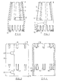
- FIG. 1 shows the side view of a socket, which is made of a piece of sheet metal by punching and bending.
- a ring element 1 is present, the formerly facing away from each other edges are connected by means of an omega 2 closure.
- This ring element 1 has an in FIG. 1 upwardly directed edge 3, from which a plurality of contact tongues 4 go out. These reeds all have the same length and the same width.
- On the opposite side of the ring member 1 also extends a plurality of contact pins 5, which extend parallel to each other in the illustrated embodiment, are rectangular in cross-section and have a tapered front end 6.
- the contact tongues 4 are separated by longitudinal slots 7.
- the contact tongues 4 are deformed from the original rectilinear shape lying in the extension of the ring element 1 in such a way that they converge inwards from the ring element 1 in the direction of their free end 8.
- the contact tongues 4 are rectilinear. You could also have a different shape from the rectilinear shape.
- the contact pins 5 are separated by slots 9 from each other.
- FIG. 2 shows an axial section through the socket of FIG. 1 , Here it can be seen that the inner sides of the contact tongues 4 extend in the region of their free end 8 slightly concave curved.
- the at the in the Figures 1 and 2 arranged on the bottom side contact pins 5 form an attachment means 10 for attachment of the socket shown on a circuit board. If the socket is attached to a circuit board, so can from the opposite, in the Figures 1 and 2 upper side of a plug pin are inserted into the socket. It must have a diameter which is greater than the distance of the upper ends of the contact tongues from each other. Usually, the connector pins are matched to the sockets. You can now the FIG. 2 but also see that because of the relatively large length of the contact tongues of the pin also, as soon as it is plugged into the socket, can still be moved to the side, without losing the contact with the socket is lost. In other words, the pin does not need to be inserted exactly concentric with the socket in this, but it can also be slightly off to one side. So there is a certain tolerance in the production of the compound.
- connection of the socket with the circuit board can at the in the Figures 1 and 2 illustrated embodiment in a simple manner done by the circuit board at the contact pins 5 corresponding positions through holes has, into which the contact pins 5 are pressed.
- a tool at the ends or in other words at the beginning of the longitudinal slots 7, so at the free points 11 of the one-sided boundary edge 3 of the ring member 1. Since the edge 3 extends in a plane transverse to the longitudinal axis of the socket can be attacked there with a tool in a simple manner.
- a tool may, for example, be a star-shaped mandrel.
- This socket which is in the Figures 1 and 2 is shown, but can also be used together with an outer sleeve, which in the FIGS. 3 and 4 is shown.
- the representation in the FIGS. 3 and 4 is not true to the scale Figures 1 and 2 ,
- the socket and the outer sleeve are matched to one another that the outer sleeve is fitted on the socket, wherein it then rests against the outside of the ring element 1.
- outer sleeve 12 has also been made from an initially flat piece of sheet metal by punching and bending. The originally facing away from each other edges are also connected by an omega closure 13 in the upper and lower areas.
- the sleeve is bounded by a flat edge.
- the opposite edge is folded inwards, see the section of the FIG. 4 , For this folding is possible, individual notches 15 are present, between which the parts to be folded are arranged.
- the axial length of the outer sleeve 12 is dimensioned so that after assembly, the free ends 8 of the contact tongues 4 are within the axial extent of the outer sleeve 12.
- the outer sleeve 12 has on its inside projections 16, which are made by the fact that in the wall of the outer sleeve a U-shaped slot 17 is introduced, and the material of the wall is unlatched inside the chip 17 inwardly. This results in these projections with a downwardly directed shoulder surface 18.
- This shoulder surface 18 is positioned so that it begins immediately on the undeformed inner wall of the outer sleeve 12. If the outer sleeve 12 is pushed onto the socket, the projections 16 are within the longitudinal slots 7 between the contact tongues 4, and the Shoulder surfaces 18 are located on the free points 11 of the edge 3 of the ring element 1. This is at one point in FIG. 6 shown.
- the outer sleeve 12 can also serve as a tool to press the socket into the plated holes in the circuit board. Since the rounded upper edge 19 of the outer sleeve 12, see FIG. 3 and FIG. 4 , In a plane perpendicular to the insertion direction and thus is parallel to the circuit board, so can be pressed by engaging the upper edge 19 of the outer sleeve 12, the socket in the plated-through holes.
- the socket is thereby connected to the circuit board, that the contact pins five is pressed into plated through holes in the circuit board.
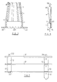
- Another type of connection shows the FIG. 5 , There, the contact pins 5 are bent right at the transition to the ring element 1 at right angles to the outside. As a result, their sides facing the printed circuit board 20 are all in one plane.
- the socket can be connected to solder pads of the circuit board in SMD. Again, the outer sleeve 12 serve to position the socket and to hold during the soldering process.
- the bending of the contact pins 5 to the outside has the advantage that the socket can be mounted concentrically with an opening in the circuit board, and that this opening is still available for other functions. If this is not necessary, it is of course also possible to bend the contact pins 5 inwards so that they do not project beyond the outside of the ring element 1.
- the folding over of the upper edge of the outer sleeve 12 leads inwards to increase the stability of the outer sleeve.
- the rounded upper edge 19 facilitates the insertion of a connector pin.
- Another function of the outer sleeve is of course that excessive deformation of the contact tongues 4 is prevented to the outside.
- the great stability of the outer sleeve 12 makes it possible to use the outer sleeve as a spacer, which is particularly useful if, for example, two circuit boards to be connected together.
- FIG. 7 shows the FIG. 7 in which is shown schematically, as three printed circuit boards 21 are arranged parallel to each other, wherein in each case between two circuit boards 21 a plurality of sockets with outer sleeves 12 are attached.
- the distance between two printed circuit boards 21 from each other corresponds to the axial length of the outer sleeve 12.
- a pin 22 is used as a pin, which is fastened with its head 23 to the lower circuit board 21. Its free end then protrudes beyond the upper circuit board 21.
- pin 24 usable, which protrudes as a smooth pin through all aligned sockets.
Landscapes
- Coupling Device And Connection With Printed Circuit (AREA)
- Multi-Conductor Connections (AREA)
Applications Claiming Priority (1)
| Application Number | Priority Date | Filing Date | Title |
|---|---|---|---|
| DE102008058204A DE102008058204A1 (de) | 2008-11-12 | 2008-11-12 | Steckbuchse |
Publications (3)
| Publication Number | Publication Date |
|---|---|
| EP2187480A2 true EP2187480A2 (fr) | 2010-05-19 |
| EP2187480A3 EP2187480A3 (fr) | 2012-09-12 |
| EP2187480B1 EP2187480B1 (fr) | 2016-03-23 |
Family
ID=41681839
Family Applications (1)
| Application Number | Title | Priority Date | Filing Date |
|---|---|---|---|
| EP09175424.2A Active EP2187480B1 (fr) | 2008-11-12 | 2009-11-09 | Douille pour carte de circuits imprimés |
Country Status (2)
| Country | Link |
|---|---|
| EP (1) | EP2187480B1 (fr) |
| DE (1) | DE102008058204A1 (fr) |
Cited By (8)
| Publication number | Priority date | Publication date | Assignee | Title |
|---|---|---|---|---|
| DE202012004650U1 (de) | 2012-05-11 | 2012-07-30 | Erni Electronics Gmbh | Steckbuchse |
| DE102012009272A1 (de) | 2012-05-11 | 2013-11-14 | Erni Electronics Gmbh & Co.Kg | Steckbuchse |
| CN104183943A (zh) * | 2013-05-28 | 2014-12-03 | 中航光电科技股份有限公司 | 支持热插拔的接触件及使用该接触件的电连接器 |
| CN108110470A (zh) * | 2018-01-26 | 2018-06-01 | 深圳市特拉利线簧端子技术有限公司 | 金属簧片结构、端子结构及电连接器 |
| EP3477781A1 (fr) * | 2017-10-30 | 2019-05-01 | Würth Elektronik ICS GmbH & Co. KG | Douille enfichable pour cartes de circuits imprimés |
| WO2019158274A1 (fr) * | 2018-02-13 | 2019-08-22 | Böllhoff Verbindungstechnik GmbH | Manchon de bras à ressort |
| EP3531510A1 (fr) * | 2018-02-23 | 2019-08-28 | Borgwarner Inc. | Ensemble de contact pour des applications de courant élevé |
| EP3568883B1 (fr) * | 2017-01-11 | 2023-12-20 | TE Connectivity Solutions GmbH | Ensemble capteur de lumière |
Families Citing this family (4)
| Publication number | Priority date | Publication date | Assignee | Title |
|---|---|---|---|---|
| DE102012106741B4 (de) * | 2012-07-25 | 2021-04-01 | Harting Electric Gmbh & Co. Kg | Kontaktelement |
| DE102015122303B3 (de) * | 2015-12-15 | 2017-04-20 | Amphenol-Tuchel Electronics Gmbh | Steckverbinderbuchse |
| DE102019124778B4 (de) * | 2019-09-16 | 2021-08-05 | Lisa Dräxlmaier GmbH | Durchkontaktierung und Leiteranordnung mit einer solchen Durchkontaktierung sowie Verfahren zur Herstellung einer solchen Durchkontaktierung |
| DE102021202438A1 (de) * | 2021-03-12 | 2022-09-15 | Knorr-Bremse Systeme für Nutzfahrzeuge GmbH | Klemmhülse zur montage eines drehfühlers sowie drehfühleranordnung und drehfühlersystem mit einer solchen klemmhülse |
Citations (1)
| Publication number | Priority date | Publication date | Assignee | Title |
|---|---|---|---|---|
| US4734064A (en) | 1986-08-29 | 1988-03-29 | Amphenol Corporation | Electrical socket contact with convex engaging tines |
Family Cites Families (12)
| Publication number | Priority date | Publication date | Assignee | Title |
|---|---|---|---|---|
| DE1465682A1 (de) * | 1964-10-01 | 1969-04-17 | Harting Elektro W | Kontaktbuchse fuer elektrische Steckverbindungen |
| US3543215A (en) * | 1968-06-28 | 1970-11-24 | Robert W Jones | Pin sockets for electronic circuit devices |
| US3564487A (en) * | 1969-02-03 | 1971-02-16 | Itt | Contact member for electrical connector |
| DE8323003U1 (de) * | 1983-08-10 | 1983-12-01 | Stocko Metallwarenfabriken Henkels Und Sohn Gmbh & Co, 5600 Wuppertal | Steckbuchse |
| US4813881A (en) * | 1986-12-29 | 1989-03-21 | Labinal Components And Systems, Inc. | Variable insertion force contact |
| WO1993016509A1 (fr) * | 1992-02-12 | 1993-08-19 | Connector Systems Technology N.V. | Borne femelle |
| US5997367A (en) * | 1995-06-05 | 1999-12-07 | Vlt Corporation | Adapter |
| CH694416A5 (de) * | 1998-08-25 | 2004-12-31 | Feller Ag | Kontaktfeder sowie Steckdose mit derselben. |
| US6155887A (en) * | 1999-05-27 | 2000-12-05 | Airborn, Inc. | Stackable connector system and contact for use therein |
| US6623279B2 (en) * | 1999-07-15 | 2003-09-23 | Incep Technologies, Inc. | Separable power delivery connector |
| US20040043644A1 (en) * | 1999-11-02 | 2004-03-04 | Dibene J. Ted | Coaxial and linear power delivery devices |
| FR2889625B1 (fr) * | 2005-08-04 | 2014-01-24 | Souriau | Element de contact femelle et procede de realisation d'un element de contact femelle |
-
2008
- 2008-11-12 DE DE102008058204A patent/DE102008058204A1/de not_active Withdrawn
-
2009
- 2009-11-09 EP EP09175424.2A patent/EP2187480B1/fr active Active
Patent Citations (1)
| Publication number | Priority date | Publication date | Assignee | Title |
|---|---|---|---|---|
| US4734064A (en) | 1986-08-29 | 1988-03-29 | Amphenol Corporation | Electrical socket contact with convex engaging tines |
Cited By (15)
| Publication number | Priority date | Publication date | Assignee | Title |
|---|---|---|---|---|
| DE102012009272B4 (de) | 2012-05-11 | 2021-08-19 | Erni Production Gmbh & Co. Kg | Steckbuchse |
| DE102012009272A1 (de) | 2012-05-11 | 2013-11-14 | Erni Electronics Gmbh & Co.Kg | Steckbuchse |
| DE202012004650U1 (de) | 2012-05-11 | 2012-07-30 | Erni Electronics Gmbh | Steckbuchse |
| CN104183943A (zh) * | 2013-05-28 | 2014-12-03 | 中航光电科技股份有限公司 | 支持热插拔的接触件及使用该接触件的电连接器 |
| EP3568883B1 (fr) * | 2017-01-11 | 2023-12-20 | TE Connectivity Solutions GmbH | Ensemble capteur de lumière |
| EP3477781A1 (fr) * | 2017-10-30 | 2019-05-01 | Würth Elektronik ICS GmbH & Co. KG | Douille enfichable pour cartes de circuits imprimés |
| DE102017125505A1 (de) | 2017-10-30 | 2019-05-02 | Würth Elektronik Ics Gmbh & Co. Kg | Steckerbuchse für Leiterplatinen |
| CN108110470A (zh) * | 2018-01-26 | 2018-06-01 | 深圳市特拉利线簧端子技术有限公司 | 金属簧片结构、端子结构及电连接器 |
| CN108110470B (zh) * | 2018-01-26 | 2024-05-24 | 深圳市特拉利线簧端子技术有限公司 | 金属簧片结构、端子结构及电连接器 |
| WO2019158274A1 (fr) * | 2018-02-13 | 2019-08-22 | Böllhoff Verbindungstechnik GmbH | Manchon de bras à ressort |
| US11511333B2 (en) | 2018-02-13 | 2022-11-29 | Böllhoff Verbindungstechnik GmbH | Spring arm sleeve |
| US10707599B2 (en) | 2018-02-23 | 2020-07-07 | Borgwarner Inc. | Contact assembly for high-current applications |
| CN110190426B (zh) * | 2018-02-23 | 2022-11-18 | 博格华纳公司 | 用于高电流应用的触头组件 |
| CN110190426A (zh) * | 2018-02-23 | 2019-08-30 | 博格华纳公司 | 用于高电流应用的触头组件 |
| EP3531510A1 (fr) * | 2018-02-23 | 2019-08-28 | Borgwarner Inc. | Ensemble de contact pour des applications de courant élevé |
Also Published As
| Publication number | Publication date |
|---|---|
| EP2187480A3 (fr) | 2012-09-12 |
| EP2187480B1 (fr) | 2016-03-23 |
| DE102008058204A1 (de) | 2010-05-20 |
Similar Documents
| Publication | Publication Date | Title |
|---|---|---|
| EP2187480B1 (fr) | Douille pour carte de circuits imprimés | |
| EP2430892B1 (fr) | Connexion de plaquettes | |
| EP3446366B1 (fr) | Contact enfichable | |
| EP3375048B1 (fr) | Contact à enficher | |
| EP2852003B1 (fr) | Élément de contact pour un connecteur à fiche | |
| EP1429423B1 (fr) | Connecteur électrique à fiche ayant un boîtier et un contact à courant fort | |
| EP3446367B1 (fr) | Contact enfichable | |
| DE102009019699B4 (de) | Anschlussklemme für Leiterplatten | |
| EP0852826B1 (fr) | Dispositif pour raccorder un connecteur coaxial a une carte de circuits par la technologie des composants montes en surface | |
| DE3220781A1 (de) | Kontaktelement zur loetfreien befestigung in leiterplatten-bohrungen | |
| DE102007055040A1 (de) | Kontaktelement und Verfahren zur Herstellung eines Kontaktelementes | |
| DE102010005833A1 (de) | Einlötkontaktanordnung | |
| DE102014111433A1 (de) | Stiftanschlussbaugruppe | |
| DE202017101396U1 (de) | Rundsteckverbinderbuchse für eine daran anordenbare Leiterplatte | |
| EP3375047B1 (fr) | Contact à insérer et méthode de fabrication d'un contact à insérer | |
| EP1671399B1 (fr) | Raccordement d'element de blindage | |
| DE202016008242U1 (de) | Steckkontakt | |
| EP1804338B1 (fr) | Douille de contact pour une fiche | |
| DE102008058203A1 (de) | Steckbuchse für Leiterplatten | |
| DE102005016265B4 (de) | Arretierung eines Rastelements mit Radsok-Buchse | |
| DE202014103718U1 (de) | Stiftanschlussbaugruppe | |
| DE102008062597B3 (de) | Verbindungselement mit mindestens einem elektrischen Steckkontakt und Verfahen zur Herstellung desselben | |
| DE102005054590A1 (de) | Elektrischer Steckverbinder | |
| DE202016102148U1 (de) | Steckkontakt | |
| EP4690382A1 (fr) | Connecteur enfichable blindé à contact de mise à la terre et son procédé d'assemblage |
Legal Events
| Date | Code | Title | Description |
|---|---|---|---|
| PUAI | Public reference made under article 153(3) epc to a published international application that has entered the european phase |
Free format text: ORIGINAL CODE: 0009012 |
|
| AK | Designated contracting states |
Kind code of ref document: A2 Designated state(s): AT BE BG CH CY CZ DE DK EE ES FI FR GB GR HR HU IE IS IT LI LT LU LV MC MK MT NL NO PL PT RO SE SI SK SM TR |
|
| AX | Request for extension of the european patent |
Extension state: AL BA RS |
|
| PUAL | Search report despatched |
Free format text: ORIGINAL CODE: 0009013 |
|
| AK | Designated contracting states |
Kind code of ref document: A3 Designated state(s): AT BE BG CH CY CZ DE DK EE ES FI FR GB GR HR HU IE IS IT LI LT LU LV MC MK MT NL NO PL PT RO SE SI SK SM TR |
|
| AX | Request for extension of the european patent |
Extension state: AL BA RS |
|
| 17P | Request for examination filed |
Effective date: 20130311 |
|
| 17Q | First examination report despatched |
Effective date: 20150224 |
|
| REG | Reference to a national code |
Ref country code: DE Ref legal event code: R079 Ref document number: 502009012288 Country of ref document: DE Free format text: PREVIOUS MAIN CLASS: H01R0012320000 Ipc: H01R0012520000 |
|
| GRAP | Despatch of communication of intention to grant a patent |
Free format text: ORIGINAL CODE: EPIDOSNIGR1 |
|
| RIC1 | Information provided on ipc code assigned before grant |
Ipc: H01R 12/52 20110101AFI20150916BHEP Ipc: H01R 13/187 20060101ALI20150916BHEP |
|
| INTG | Intention to grant announced |
Effective date: 20151002 |
|
| GRAS | Grant fee paid |
Free format text: ORIGINAL CODE: EPIDOSNIGR3 |
|
| GRAA | (expected) grant |
Free format text: ORIGINAL CODE: 0009210 |
|
| AK | Designated contracting states |
Kind code of ref document: B1 Designated state(s): AT BE BG CH CY CZ DE DK EE ES FI FR GB GR HR HU IE IS IT LI LT LU LV MC MK MT NL NO PL PT RO SE SI SK SM TR |
|
| REG | Reference to a national code |
Ref country code: GB Ref legal event code: FG4D Free format text: NOT ENGLISH |
|
| REG | Reference to a national code |
Ref country code: CH Ref legal event code: EP |
|
| REG | Reference to a national code |
Ref country code: AT Ref legal event code: REF Ref document number: 783966 Country of ref document: AT Kind code of ref document: T Effective date: 20160415 |
|
| REG | Reference to a national code |
Ref country code: IE Ref legal event code: FG4D Free format text: LANGUAGE OF EP DOCUMENT: GERMAN |
|
| REG | Reference to a national code |
Ref country code: DE Ref legal event code: R096 Ref document number: 502009012288 Country of ref document: DE |
|
| REG | Reference to a national code |
Ref country code: LT Ref legal event code: MG4D |
|
| REG | Reference to a national code |
Ref country code: NL Ref legal event code: MP Effective date: 20160323 |
|
| PG25 | Lapsed in a contracting state [announced via postgrant information from national office to epo] |
Ref country code: FI Free format text: LAPSE BECAUSE OF FAILURE TO SUBMIT A TRANSLATION OF THE DESCRIPTION OR TO PAY THE FEE WITHIN THE PRESCRIBED TIME-LIMIT Effective date: 20160323 Ref country code: GR Free format text: LAPSE BECAUSE OF FAILURE TO SUBMIT A TRANSLATION OF THE DESCRIPTION OR TO PAY THE FEE WITHIN THE PRESCRIBED TIME-LIMIT Effective date: 20160624 Ref country code: NO Free format text: LAPSE BECAUSE OF FAILURE TO SUBMIT A TRANSLATION OF THE DESCRIPTION OR TO PAY THE FEE WITHIN THE PRESCRIBED TIME-LIMIT Effective date: 20160623 |
|
| PG25 | Lapsed in a contracting state [announced via postgrant information from national office to epo] |
Ref country code: SE Free format text: LAPSE BECAUSE OF FAILURE TO SUBMIT A TRANSLATION OF THE DESCRIPTION OR TO PAY THE FEE WITHIN THE PRESCRIBED TIME-LIMIT Effective date: 20160323 Ref country code: LT Free format text: LAPSE BECAUSE OF FAILURE TO SUBMIT A TRANSLATION OF THE DESCRIPTION OR TO PAY THE FEE WITHIN THE PRESCRIBED TIME-LIMIT Effective date: 20160323 Ref country code: LV Free format text: LAPSE BECAUSE OF FAILURE TO SUBMIT A TRANSLATION OF THE DESCRIPTION OR TO PAY THE FEE WITHIN THE PRESCRIBED TIME-LIMIT Effective date: 20160323 Ref country code: NL Free format text: LAPSE BECAUSE OF FAILURE TO SUBMIT A TRANSLATION OF THE DESCRIPTION OR TO PAY THE FEE WITHIN THE PRESCRIBED TIME-LIMIT Effective date: 20160323 |
|
| PG25 | Lapsed in a contracting state [announced via postgrant information from national office to epo] |
Ref country code: EE Free format text: LAPSE BECAUSE OF FAILURE TO SUBMIT A TRANSLATION OF THE DESCRIPTION OR TO PAY THE FEE WITHIN THE PRESCRIBED TIME-LIMIT Effective date: 20160323 Ref country code: PL Free format text: LAPSE BECAUSE OF FAILURE TO SUBMIT A TRANSLATION OF THE DESCRIPTION OR TO PAY THE FEE WITHIN THE PRESCRIBED TIME-LIMIT Effective date: 20160323 Ref country code: IS Free format text: LAPSE BECAUSE OF FAILURE TO SUBMIT A TRANSLATION OF THE DESCRIPTION OR TO PAY THE FEE WITHIN THE PRESCRIBED TIME-LIMIT Effective date: 20160723 |
|
| PG25 | Lapsed in a contracting state [announced via postgrant information from national office to epo] |
Ref country code: RO Free format text: LAPSE BECAUSE OF FAILURE TO SUBMIT A TRANSLATION OF THE DESCRIPTION OR TO PAY THE FEE WITHIN THE PRESCRIBED TIME-LIMIT Effective date: 20160323 Ref country code: PT Free format text: LAPSE BECAUSE OF FAILURE TO SUBMIT A TRANSLATION OF THE DESCRIPTION OR TO PAY THE FEE WITHIN THE PRESCRIBED TIME-LIMIT Effective date: 20160725 Ref country code: CZ Free format text: LAPSE BECAUSE OF FAILURE TO SUBMIT A TRANSLATION OF THE DESCRIPTION OR TO PAY THE FEE WITHIN THE PRESCRIBED TIME-LIMIT Effective date: 20160323 Ref country code: SK Free format text: LAPSE BECAUSE OF FAILURE TO SUBMIT A TRANSLATION OF THE DESCRIPTION OR TO PAY THE FEE WITHIN THE PRESCRIBED TIME-LIMIT Effective date: 20160323 Ref country code: SM Free format text: LAPSE BECAUSE OF FAILURE TO SUBMIT A TRANSLATION OF THE DESCRIPTION OR TO PAY THE FEE WITHIN THE PRESCRIBED TIME-LIMIT Effective date: 20160323 Ref country code: ES Free format text: LAPSE BECAUSE OF FAILURE TO SUBMIT A TRANSLATION OF THE DESCRIPTION OR TO PAY THE FEE WITHIN THE PRESCRIBED TIME-LIMIT Effective date: 20160323 |
|
| PG25 | Lapsed in a contracting state [announced via postgrant information from national office to epo] |
Ref country code: IT Free format text: LAPSE BECAUSE OF FAILURE TO SUBMIT A TRANSLATION OF THE DESCRIPTION OR TO PAY THE FEE WITHIN THE PRESCRIBED TIME-LIMIT Effective date: 20160323 |
|
| REG | Reference to a national code |
Ref country code: DE Ref legal event code: R097 Ref document number: 502009012288 Country of ref document: DE |
|
| PLBE | No opposition filed within time limit |
Free format text: ORIGINAL CODE: 0009261 |
|
| STAA | Information on the status of an ep patent application or granted ep patent |
Free format text: STATUS: NO OPPOSITION FILED WITHIN TIME LIMIT |
|
| PG25 | Lapsed in a contracting state [announced via postgrant information from national office to epo] |
Ref country code: DK Free format text: LAPSE BECAUSE OF FAILURE TO SUBMIT A TRANSLATION OF THE DESCRIPTION OR TO PAY THE FEE WITHIN THE PRESCRIBED TIME-LIMIT Effective date: 20160323 |
|
| PG25 | Lapsed in a contracting state [announced via postgrant information from national office to epo] |
Ref country code: BG Free format text: LAPSE BECAUSE OF FAILURE TO SUBMIT A TRANSLATION OF THE DESCRIPTION OR TO PAY THE FEE WITHIN THE PRESCRIBED TIME-LIMIT Effective date: 20160623 Ref country code: BE Free format text: LAPSE BECAUSE OF NON-PAYMENT OF DUE FEES Effective date: 20161130 |
|
| 26N | No opposition filed |
Effective date: 20170102 |
|
| PG25 | Lapsed in a contracting state [announced via postgrant information from national office to epo] |
Ref country code: SI Free format text: LAPSE BECAUSE OF FAILURE TO SUBMIT A TRANSLATION OF THE DESCRIPTION OR TO PAY THE FEE WITHIN THE PRESCRIBED TIME-LIMIT Effective date: 20160323 |
|
| REG | Reference to a national code |
Ref country code: CH Ref legal event code: PL |
|
| GBPC | Gb: european patent ceased through non-payment of renewal fee |
Effective date: 20161109 |
|
| PG25 | Lapsed in a contracting state [announced via postgrant information from national office to epo] |
Ref country code: LI Free format text: LAPSE BECAUSE OF NON-PAYMENT OF DUE FEES Effective date: 20161130 Ref country code: CH Free format text: LAPSE BECAUSE OF NON-PAYMENT OF DUE FEES Effective date: 20161130 |
|
| REG | Reference to a national code |
Ref country code: IE Ref legal event code: MM4A |
|
| REG | Reference to a national code |
Ref country code: FR Ref legal event code: ST Effective date: 20170731 |
|
| PG25 | Lapsed in a contracting state [announced via postgrant information from national office to epo] |
Ref country code: LU Free format text: LAPSE BECAUSE OF NON-PAYMENT OF DUE FEES Effective date: 20161130 |
|
| PG25 | Lapsed in a contracting state [announced via postgrant information from national office to epo] |
Ref country code: FR Free format text: LAPSE BECAUSE OF NON-PAYMENT OF DUE FEES Effective date: 20161130 |
|
| PG25 | Lapsed in a contracting state [announced via postgrant information from national office to epo] |
Ref country code: IE Free format text: LAPSE BECAUSE OF NON-PAYMENT OF DUE FEES Effective date: 20161109 Ref country code: GB Free format text: LAPSE BECAUSE OF NON-PAYMENT OF DUE FEES Effective date: 20161109 |
|
| REG | Reference to a national code |
Ref country code: AT Ref legal event code: MM01 Ref document number: 783966 Country of ref document: AT Kind code of ref document: T Effective date: 20161109 |
|
| PG25 | Lapsed in a contracting state [announced via postgrant information from national office to epo] |
Ref country code: AT Free format text: LAPSE BECAUSE OF NON-PAYMENT OF DUE FEES Effective date: 20161109 |
|
| REG | Reference to a national code |
Ref country code: BE Ref legal event code: MM Effective date: 20161130 |
|
| PG25 | Lapsed in a contracting state [announced via postgrant information from national office to epo] |
Ref country code: HU Free format text: LAPSE BECAUSE OF FAILURE TO SUBMIT A TRANSLATION OF THE DESCRIPTION OR TO PAY THE FEE WITHIN THE PRESCRIBED TIME-LIMIT; INVALID AB INITIO Effective date: 20091109 Ref country code: CY Free format text: LAPSE BECAUSE OF FAILURE TO SUBMIT A TRANSLATION OF THE DESCRIPTION OR TO PAY THE FEE WITHIN THE PRESCRIBED TIME-LIMIT Effective date: 20160323 |
|
| PG25 | Lapsed in a contracting state [announced via postgrant information from national office to epo] |
Ref country code: TR Free format text: LAPSE BECAUSE OF FAILURE TO SUBMIT A TRANSLATION OF THE DESCRIPTION OR TO PAY THE FEE WITHIN THE PRESCRIBED TIME-LIMIT Effective date: 20160323 Ref country code: MK Free format text: LAPSE BECAUSE OF FAILURE TO SUBMIT A TRANSLATION OF THE DESCRIPTION OR TO PAY THE FEE WITHIN THE PRESCRIBED TIME-LIMIT Effective date: 20160323 Ref country code: HR Free format text: LAPSE BECAUSE OF FAILURE TO SUBMIT A TRANSLATION OF THE DESCRIPTION OR TO PAY THE FEE WITHIN THE PRESCRIBED TIME-LIMIT Effective date: 20160323 Ref country code: MC Free format text: LAPSE BECAUSE OF FAILURE TO SUBMIT A TRANSLATION OF THE DESCRIPTION OR TO PAY THE FEE WITHIN THE PRESCRIBED TIME-LIMIT Effective date: 20160323 |
|
| PG25 | Lapsed in a contracting state [announced via postgrant information from national office to epo] |
Ref country code: MT Free format text: LAPSE BECAUSE OF FAILURE TO SUBMIT A TRANSLATION OF THE DESCRIPTION OR TO PAY THE FEE WITHIN THE PRESCRIBED TIME-LIMIT Effective date: 20160323 |
|
| PGFP | Annual fee paid to national office [announced via postgrant information from national office to epo] |
Ref country code: DE Payment date: 20251119 Year of fee payment: 17 |