EP2187543B1 - Vorrichtung zum Senden und Empfangen eines Signals und Verfahren zum Senden und Empfangen eines Signals - Google Patents
Vorrichtung zum Senden und Empfangen eines Signals und Verfahren zum Senden und Empfangen eines Signals Download PDFInfo
- Publication number
- EP2187543B1 EP2187543B1 EP09161830A EP09161830A EP2187543B1 EP 2187543 B1 EP2187543 B1 EP 2187543B1 EP 09161830 A EP09161830 A EP 09161830A EP 09161830 A EP09161830 A EP 09161830A EP 2187543 B1 EP2187543 B1 EP 2187543B1
- Authority
- EP
- European Patent Office
- Prior art keywords
- block
- data
- preamble
- signaling
- header
- Prior art date
- Legal status (The legal status is an assumption and is not a legal conclusion. Google has not performed a legal analysis and makes no representation as to the accuracy of the status listed.)
- Active
Links
Images



























Classifications
-
- H—ELECTRICITY
- H04—ELECTRIC COMMUNICATION TECHNIQUE
- H04L—TRANSMISSION OF DIGITAL INFORMATION, e.g. TELEGRAPHIC COMMUNICATION
- H04L5/00—Arrangements affording multiple use of the transmission path
- H04L5/0001—Arrangements for dividing the transmission path
- H04L5/0003—Two-dimensional division
- H04L5/0005—Time-frequency
- H04L5/0007—Time-frequency the frequencies being orthogonal, e.g. OFDM(A) or DMT
-
- H—ELECTRICITY
- H04—ELECTRIC COMMUNICATION TECHNIQUE
- H04L—TRANSMISSION OF DIGITAL INFORMATION, e.g. TELEGRAPHIC COMMUNICATION
- H04L1/00—Arrangements for detecting or preventing errors in the information received
- H04L1/004—Arrangements for detecting or preventing errors in the information received by using forward error control
- H04L1/0056—Systems characterized by the type of code used
- H04L1/0057—Block codes
-
- H—ELECTRICITY
- H04—ELECTRIC COMMUNICATION TECHNIQUE
- H04L—TRANSMISSION OF DIGITAL INFORMATION, e.g. TELEGRAPHIC COMMUNICATION
- H04L1/00—Arrangements for detecting or preventing errors in the information received
- H04L1/004—Arrangements for detecting or preventing errors in the information received by using forward error control
- H04L1/0056—Systems characterized by the type of code used
- H04L1/0071—Use of interleaving
-
- H—ELECTRICITY
- H04—ELECTRIC COMMUNICATION TECHNIQUE
- H04L—TRANSMISSION OF DIGITAL INFORMATION, e.g. TELEGRAPHIC COMMUNICATION
- H04L27/00—Modulated-carrier systems
- H04L27/26—Systems using multi-frequency codes
- H04L27/2601—Multicarrier modulation systems
- H04L27/2602—Signal structure
-
- H—ELECTRICITY
- H04—ELECTRIC COMMUNICATION TECHNIQUE
- H04L—TRANSMISSION OF DIGITAL INFORMATION, e.g. TELEGRAPHIC COMMUNICATION
- H04L27/00—Modulated-carrier systems
- H04L27/32—Carrier systems characterised by combinations of two or more of the types covered by groups H04L27/02, H04L27/10, H04L27/18 or H04L27/26
- H04L27/34—Amplitude- and phase-modulated carrier systems, e.g. quadrature-amplitude modulated carrier systems
-
- H—ELECTRICITY
- H04—ELECTRIC COMMUNICATION TECHNIQUE
- H04L—TRANSMISSION OF DIGITAL INFORMATION, e.g. TELEGRAPHIC COMMUNICATION
- H04L5/00—Arrangements affording multiple use of the transmission path
- H04L5/003—Arrangements for allocating sub-channels of the transmission path
- H04L5/0044—Allocation of payload; Allocation of data channels, e.g. PDSCH or PUSCH
-
- H—ELECTRICITY
- H04—ELECTRIC COMMUNICATION TECHNIQUE
- H04L—TRANSMISSION OF DIGITAL INFORMATION, e.g. TELEGRAPHIC COMMUNICATION
- H04L5/00—Arrangements affording multiple use of the transmission path
- H04L5/003—Arrangements for allocating sub-channels of the transmission path
- H04L5/0048—Allocation of pilot signals, i.e. of signals known to the receiver
- H04L5/005—Allocation of pilot signals, i.e. of signals known to the receiver of common pilots, i.e. pilots destined for multiple users or terminals
-
- H—ELECTRICITY
- H04—ELECTRIC COMMUNICATION TECHNIQUE
- H04L—TRANSMISSION OF DIGITAL INFORMATION, e.g. TELEGRAPHIC COMMUNICATION
- H04L5/00—Arrangements affording multiple use of the transmission path
- H04L5/003—Arrangements for allocating sub-channels of the transmission path
- H04L5/0053—Allocation of signalling, i.e. of overhead other than pilot signals
Definitions
- the present invention relates to a method for transmitting and receiving a signal and an apparatus for transmitting and receiving a signal, and more particularly, to a method for transmitting and receiving a signal and an apparatus for transmitting and receiving a signal, which are capable of improving data transmission efficiency.
- a digital television (DTV) system can receive a digital broadcasting signal and provide a variety of supplementary services to users as well as a video signal and an audio signal.
- Digital Video Broadcasting (DVB)-C2 is the third specification to join DVB's family of second generation transmission systems. Developed in 1994, today DVB-C is deployed in more than 50 million cable tuners worldwide. In line with the other DVB second generation systems, DVB-C2 uses a combination of Low-density parity-check (LDPC) and BCH codes. This powerful Forward Error correction (FEC) provides about 5dB improvement of carrier-to-noise ratio over DVB-C. Appropriate bit-interleaving schemes optimize the overall robustness of the FEC system. Extended by a header, these frames are called Physical Layer Pipes (PLP). One or more of these PLPs are multiplexed into a data slice. Two dimensional interleaving (in the time and frequency domains) is applied to each slice enabling the receiver to eliminate the impact of burst impairments and frequency selective interference such as single frequency ingress.
- PLP Physical Layer Pipes
- the present invention is directed to a method for transmitting and receiving a signal and an apparatus for transmitting and receiving a signal that substantially obviate one or more problems due to limitations and disadvantages of the related art.
- An object of the present invention is to provide a method of transmitting broadcasting signal to a receiver, according to claim 1.
- Another aspect of the present invention provides a method of receiving broadcasting signal, according to claim 4.
- Yet another aspect of the present invention provides a transmitter of transmitting broadcasting signal to a receiver, according to claim 8.
- Yet another aspect of the present invention provides a receiver of receiving broadcasting signal, according to claim 11.
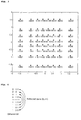
- Fig. 1 is an example of 64- Quadrature amplitude modulation (QAM) used in European DVB-T.
- QAM Quadrature amplitude modulation
- Fig. 2 is a method of Binary Reflected Gray Code (BRGC).
- BRGC Binary Reflected Gray Code
- Fig. 3 is an output close to Gaussian by modifying 64-QAM used in DVB-T.
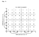
- Fig. 4 is Hamming distance between Reflected pair in BRGC.
- Fig. 5 is characteristics in QAM where Reflected pair exists for each I axis and Q axis.
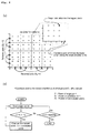
- Fig. 6 is a method of modifying QAM using Reflected pair of BRGC.
- Fig. 7 is an example of modified 64/256/1024/4096-QAM.
- Figs. 8-9 are an example of modified 64-QAM using Reflected Pair of BRGC.
- Figs. 10-11 are an example of modified 256-QAM using Reflected Pair of BRGC.
- Figs. 12-13 are an example of modified 1024-QAM using Reflected Pair of BRGC(0 ⁇ 511).
- Figs. 14-15 are an example of modified 1024-QAM using Reflected Pair of BRGC(512 ⁇ 1023).
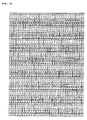
- Figs. 16-17 are an example of modified 4096-QAM using Reflected Pair of BRGC(0 ⁇ 511).
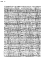
- Figs. 20-21 are an example of modified 4096-QAM using Reflected Pair of BRGC(1024 ⁇ 1535).
- Figs. 24-25 are an example of modified 4096-QAM using Reflected Pair of BRGC(2048 ⁇ 2559).
- Figs. 26-27 are an example of modified 4096-QAM using Reflected Pair of BRGC(2560 ⁇ 3071).
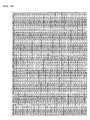
- Figs. 28-29 are an example of modified 4096-QAM using Reflected Pair of BRGC(3072 ⁇ 3583).
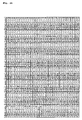
- Figs. 30-31 are an example of modified 4096-QAM using Reflected Pair of BRGC(3584 ⁇ 4095).
- Fig. 33 is an example of transformation of MQAM into Non-uniform constellation.
- Fig. 35 is an example of an input processor.
- Fig. 36 is an information that can be included in Base band (BB).
- Fig. 38 is an example of shortened/punctured encoder.
- Fig. 39 is an example of applying various constellations.
- Fig. 40 is another example of cases where compatibility between conventional systems is considered.
- Fig. 41 is a frame structure which comprises preamble for L1 signaling and data symbol for PLP data.
- Fig. 42 is an example of frame builder.
- Fig. 43 is an example of pilot insert (404) shown in Fig. 4 .
- Fig. 44 is a structure of SP.
- Fig. 45 is a new SP structure or Pilot Pattern (PP) 5'.
- Fig. 47 is a relationship between data symbol and preamble.
- Fig. 51 is an example of modulator based on OFDM.
- Fig. 52 is an example of preamble structure.
- Fig. 53 is an example of Preamble decoding.
- Fig. 54 is a process for designing more optimized preamble.
- Fig. 55 is another example of preamble structure
- Fig. 56 is another example of Preamble decoding.
- Fig. 57 is an example of Preamble structure.
- Fig. 60 is an example of digital receiver system.
- Fig. 61 is an example of analog processor used at receiver.
- Fig. 62 is an example of demodulator.
- Fig. 63 is an example of frame parser.
- Fig. 64 is an example of BICM demodulator.
- Fig. 66 is an example of output processor.
- Fig. 68 is an example of L1 block repetition rate of 8 MHz.
- Fig. 69 is a new L1 block repetition rate of 7.61 MHz.
- Fig. 72 is an example of symbol interleaver.
- Fig. 74 is another example of L1 signaling transmitted within a frame header.
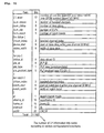
- Fig. 76 is a table analyzing overhead of L1 signaling which is transmitted in FECFRAME header at ModCod Header Insert (307) on data path of BICM module shown in Fig. 3 .
- Fig. 77 is showing a structure for FECFRAME header for minimizing overhead.
- Fig. 79 is showing examples of a transmission frame and FEC frame structure.
- Fig. 80 is showing an example of L1 signaling.
- Fig. 82 is showing a structure of L1 signaling block.
- Fig. 83 is showing an L1 time interleaving.
- Fig. 84 is showing an example of extracting modulation and code information.
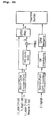
- Fig. 85 is showing another example of L1-pre signaling.
- Fig. 86 is showing an example of scheduling of L1 signaling block that is transmitted in preamble.
- Fig. 87 is showing an example of L1-pre signaling where power boosting is considered.
- Fig 88 is showing an example of L1 signaling.
- Fig. 89 is showing another example of extracting modulation and code information.
- Fig. 92 is showing an example of L1-pre signaling.
- Fig. 93 is showing an example of L1 signaling.
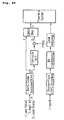
- Fig. 94 is showing an example of L1 signalling path.
- service is indicative of either broadcast contents which can be transmitted/received by the signal transmission/reception apparatus.
- Quadrature amplitude modulation using Binary Reflected Gray Code (BRGC) is used as modulation in a broadcasting transmission environment where conventional Bit Interleaved Coded Modulation (BICM) is used.
- BICM Bit Interleaved Coded Modulation
- Fig. 1 shows an example of 64-QAM used in European DVB-T.
- Fig. 6 shows a method of modifying QAM using Reflected pair of BRGC.
- Fig. 6a shows a constellation and
- Fig. 6b shows a flowchart for modifying QAM using Reflected pair of BRGC.
- a target point which has the highest power among constellation points needs to be found.
- Candidate points are points where that target point can move and are the closest neighbor points of the target point's reflected pair.
- an empty point i.e., a point which is not yet taken by other points
- the power of the target point and the power of a candidate point are compared. If the power of the candidate point is smaller, the target point moves to the candidate point.
- Fig. 32 shows an example of Bit mapping of Modified-QAM where 256-QAM is modified using BRGC.
- Fig. 32a and Fig. 32b show mapping of Most Significant Bits (MSB). Points designated as filled circles represent mappings of ones and points designated as blank circles represent mappings of zeros. In a same manner, each bit is mapped as shown in figures from (a) through (h) in Fig. 32 , until Least Significant Bits(LSB) are mapped.
- Modified-QAM can enable bit decision using only I or Q axes as conventional QAM, except for a bit which is next to MSB ( Fig. 32c and Fig. 32d ).
- a simple receiver can be made by partially modifying a receiver for QAM.
- An efficient receiver can be implemented by checking both I and Q values only when determining bit next to MSB and by calculating only I or Q for the rest of bits. This method can be applied to Approximate LLR, Exact LLR, or Hard decision.
- Non-uniform constellation or NU-MQAM can be made.
- Pj can be modified to fit MQAM.
- MQAM two PAMs having I axis and Q axis can be considered.
- the number of points changes in MQAM.
- Fig. 35 shows an example of an input processor.
- Input MPEG-TS or GSE stream can be transformed by input preprocessor into a total of n streams which will be independently processed.
- Each of those streams can be either a complete TS frame which includes multiple service components or a minimum TS frame which includes service component (i.e., video or audio).
- each of those streams can be a GSE stream which transmits either multiple services or a single service.
- a Merger/slicer module 208 can perform BB frame slicing from each PLP, merging BB frames from multiple PLPs, and scheduling each BB frame within a transmission frame. Therefore, the merger/slicer module 208 can output L1 signaling information which relates to allocation of PLP in frame.
- a BB scrambler module 209 can randomize input bitstreams to minimize correlation between bits within bitstreams.
- the modules in shadow in Fig. 35 are modules used when transmission system uses a single PLP, the other modules in Fig. 35 are modules used when the transmission device uses multiple PLPs.
- the ModCod Header inserting module 307 shown in Fig. 37 can take Adaptive coding and modulation (ACM)/Variable coding and modulation (VCM) feedback information and add parameter information used in coding and modulation to a FEC block as header.
- ACM Adaptive coding and modulation
- VCM Variariable coding and modulation
- the Modulation type/Coderate (ModCod) header can include the following information:
- Fig. 38 shows an example of LDPC encoding using shortening / puncturing.
- Shortening process can be performed on input blocks which have less bits than a required number of bits for LDPC encoding as many zero bits required for LDPC encoding can be padded (301c).
- Zero Padded input bitstreams can have parity bits through LDPC encoding (302c).
- bitstreams that correspond to original bitstreams zeros can be removed (303c) and for parity bitstreams, puncturing (304c) can be performed according to code-rates.
- These processed information bitstreams and parity bitstreams can be multiplexed into original sequences and outputted (305c).
- Fig. 41 shows a frame structure which comprises preamble for L1 signaling and data symbol for PLP data. It can be seen that preamble and data symbols are cyclically generated, using one frame as a unit. Data symbols comprise PLP type 0 which is transmitted using a fixed modulation/coding and PLP type 1 which is transmitted using a variable modulation/coding. For PLP type 0, information such as modulation, FEC type, and FEC code rate are transmitted in preamble (see Fig. 42 Frame header insert 401). For PLP type 1, corresponding information can be transmitted in FEC block header of a data symbol (see Fig. 37 ModCod header insert 307).
- ModCod overhead can be reduced by 3-4% from a total transmission rate, for PLP type0 which is transmitted at a fixed bit rate.
- Frame header remover r401 shown in Fig. 63 can extract information on Modulation and FEC code rate and provide the extracted information to a BICM decoding module.
- ModCod extracting modules, r307 and r307-1 shown in Fig. 64 can extract and provide the parameters necessary for BICM decoding.
- Channel bonding environment is assumed for L1 information transmitted in Frame header and data that correspond to each data slice is defined as PLP. Therefore, information such as PLP identifier, channel bonding identifier, and PLP start address are required for each channel used in bonding.
- PLP identifier e.g., a PLP type supports variable modulation/coding
- ModCod field in Frame header if PLP type supports fixed modulation/coding to reduce signaling overhead.
- a Notch band exists for each PLP, by transmitting the start address of the Notch and its width, decoding corresponding carriers at the receiver can become unnecessary.
- Fig. 43 shows an example of Pilot Pattern 5 (PP5) applied in a channel bonding environment. As shown, if SP positions are coincident with preamble pilot positions, irregular pilot structure can occur.
- PP5 Pilot Pattern 5
- Fig. 43a shows an example of pilot inserting module 404 as shown in Fig. 42 .
- a single frequency band for example, 8 MHz
- the available bandwidth is 7.61 MHz, but if multiple frequency bands are bonded, guard bands can be removed, thus, frequency efficiency can increase greatly.
- Fig. 43b is an example of preamble inserting module 504 as shown in Fig. 51 that is transmitted at the front part of the frame and even with channel bonding, the preamble has repetition rate of 7.61 MHz, which is bandwidth of L1 block. This is a structure considering the bandwidth of a tuner which performs initial channel scanning.
- GI guard interval
- preamble pilot positions can be coincident with every SP positions of data symbol.
- data slice where a service is transmitted can be determined regardless of 8 MHz bandwidth granularity.
- transmission starting from SP position and ending at SP position can be chosen.
- channel estimation module r501 shown in Fig. 62 can perform time interpolation to obtain pilots shown in dotted lines in Fig. 43 and perform frequency interpolation.
- time interpolation to obtain pilots shown in dotted lines in Fig. 43 and perform frequency interpolation.
- intervals for non-continuous points of which intervals are designated as 32 in Fig. 43 , either performing interpolations on left and right separately or performing interpolations on only one side then performing interpolation on the other side by using the already interpolated pilot positions of which interval is 12 as a reference point can be implemented.
- data slice width can vary within 7.61 MHz, thus, a receiver can minimize power consumption by performing channel estimation and decoding only necessary subcarriers.
- preamble structure can meet the requirements such as preamble pilot positions should cover all possible SP positions for initial channel acquisition; maximum number of carriers should be 3409 (7.61 MHz) for initial scanning; exactly same pilot patterns and scrambling sequence should be used for C2 detection; and no detection-specific preamble like P1 in T2 is required.
- pilots in every preamble can be used when time interpolation of SP of data symbol is performed. Therefore, channel acquisition and channel estimation at the frame boundaries can be improved.
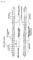
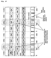
- Fig. 47 shows a relationship between data symbol and preamble when preamble structures as shown in Fig. 52 and Fig. 53 are used.
- L1 block can be repeated by period of 6 MHz.
- For L1 decoding both frequency offset and Preamble shift pattern should be found. L1 decoding is not possible in arbitrary tuner position without channel bonding information and a receiver cannot differentiate between preamble shift value and frequency offset.
- a receiver specifically for Frame header remover r401 shown in Fig. 63 to perform L1 signal decoding, channel bonding structure needs to be obtained. Because preamble shift amount expected at two vertically shadowed regions in Fig. 47 is known, time/freq synchronizing module r505 in Fig. 62 can estimate carrier frequency offset. Based on the estimation, L1 signaling path (r308-1 ⁇ r301-1) in Fig. 64 can decode L1.
- Fig. 48 shows a relationship between data symbol and preamble when the preamble structure as shown in Fig. 55 is used.
- L1 block can be repeated by period of 8 MHz.
- Frequency offset can be easily estimated by using known Pseudo Random Binary Sequence (PRBS) sequence.
- PRBS Pseudo Random Binary Sequence
- preamble and data symbols are aligned, thus, additional sync search can become unnecessary. Therefore, for a receiver, specifically for the Frame header remover module r401 shown in Fig. 63 , it is possible that only correlation peak with pilot scrambling sequence needs to be obtained to perform L1 signal decoding.
- the time/freq synchronizing module r505 in Fig. 62 can estimate carrier frequency offset from peak position.
- Slightly less delay coverage may not be an important in cable channel. For example, it can be 8 ⁇ s for PP5' and 4 ⁇ s for PP7' compared to 9.3 ⁇ s (PP5) and 4.7 ⁇ s (PP7). Meaningful delays can be covered by both pilot patterns even in a worst case. For preamble pilot position, no more than all SP positions in data symbol are necessary.
- pilot position and pattern can be repeated based on a period of 8 MHz.
- a single pilot pattern can be used for both preamble and data symbols. L1 decoding can always be possible without channel bonding knowledge.
- the proposed pilot pattern may not affect commonality with T2 because the same pilot strategy of scattered pilot pattern can be used; T2 already uses 8 different pilot patterns; and no significant receiver complexity can be increased by modified pilot patterns.
- the period of PRBS can be 2047 (m-sequence); PRBS generation can be reset every 8 MHz, of which the period is 3584; pilot repetition rate of 56 can be also co-prime with 2047; and no PAPR issue can be expected.
- Fig. 51 shows an example of a modulator based on OFDM.
- Input symbol streams can be transformed into time domain by IFFT module 501.
- PAPR peak-to-average power ratio
- ACE Active constellation extension
- GI inserting module 503 can copy a last part of effective OFDM symbol to fill guard interval in a form of cyclic prefix.
- Preamble inserting module 504 can insert preamble at the front of each transmitted frame such that a receiver can detect digital signal, frame and acquire time/freq offset acquisition. At this time, the preamble signal can perform physical layer signaling such as FFT size (3 bits) and Guard interval size (3 bits). The Preamble inserting module 504 can be omitted if the modulator is specifically for DVB-C2.
- Fig. 52 shows an example of a preamble structure for channel bonding, generated at preamble inserting module 504 in Fig. 51 .
- One complete L1 block should be "always decodable" in any arbitrary 7.61 MHz tuning window position and no loss of L1 signaling regardless of tuner window position should occur.
- L1 blocks can be repeated in frequency domain by period of 6 MHz. Data symbol can be channel bonded for every 8 MHz.
- a receiver uses a tuner such as the tuner r603 represented in Fig. 61 which uses a bandwidth of 7.61 MHz
- the Frame header remover r401 in Fig. 63 needs to rearrange the received cyclic shifted L1 block ( Fig. 53 ) to its original form. This rearrangement is possible because L1 block is repeated for every 6MHz block.
- Fig. 53a can be reordered into Fig. 53b .
- Fig. 54 shows a process for designing a more optimized preamble.
- the preamble structure of Fig. 52 uses only 6MHz of total tuner bandwidth 7.61 MHz for L1 decoding. In terms of spectrum efficiency, tuner bandwidth of 7.61 MHz is not fully utilized. Therefore, there can be further optimization in spectrum efficiency.
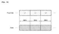
- Fig. 55 shows another example of preamble structure or preamble symbols structure for full spectrum efficiency, generated at Frame Header Inserting module 401 in Fig. 42 .
- L1 blocks can be repeated in frequency domain by period of 8 MHz.
- One complete L1 block is still "always decodable" in any arbitrary 7.61 MHz tuning window position. After tuning, the 7.61 MHz data can be regarded as a virtually punctured code. Having exactly the same bandwidth for both the preamble and data symbols and exactly the same pilot structure for both the preamble and data symbols can maximize spectrum efficiency.
- Other features such as cyclic shifted property and not sending L1 block in case of no data slice can be kept unchanged.
- the bandwidth of preamble symbols can be identical with the bandwidth of data symbols or, as shown in Fig. 57 , the bandwidth of the preamble symbols can be the bandwidth of the tuner (here, it's 7.61 MHz).
- the tuner bandwidth can be defined as a bandwidth that corresponds to a number of total active carriers when a single channel is used. That is, the bandwidth of the preamble symbol can correspond to the number of total active carriers (here, it's 7.61 MHz).
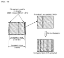
- Fig. 56 shows a virtually punctured code.
- the 7.61 MHz data among the 8 MHz L1 block can be considered as punctured coded.
- Frame header remover r401 in Fig. 63 needs to rearrange received, cyclic shifted L1 block into original form as shown in Fig. 56 .
- L1 decoding is performed using the entire bandwidth of the tuner.
- a spectrum of the rearranged L1 block can have a blank region within the spectrum as shown in upper right side of Fig. 56 because an original size of L1 block is 8 MHz bandwidth.
- the block can have a form which appears to be punctured as shown in lower right side of Fig. 56 .
- This L1 block can be decoded at the punctured/shortened decode module r303-1 in Fig. 64 .
- the entire tuner bandwidth can be utilized, thus spectrum efficiency and coding gain can be increased.
- an identical bandwidth and pilot structure can be used for the preamble and data symbols.
- the preamble bandwidth or the preamble symbols bandwidth is set as a tuner bandwidth as shown in Fig. 58 , (it's 7.61 MHz in the example), a complete L1 block can be obtained after rearrangement even without puncturing.
- the L1 block has 3408 active subcarriers and the 3408 active subcarriers correspond to 7.61 MHz of 8MHz Radio Frequency (RF) band.
- RF Radio Frequency
- the proposed new preamble structure can be advantageous in that it's fully compatible with previously used preamble except that the bandwidth is different; L1 blocks are repeated by period of 8 MHz; L1 block can be always decodable regardless of tuner window position; Full tuner bandwidth can be used for L1 decoding; maximum spectrum efficiency can guarantee more coding gain; incomplete L1 block can be considered as punctured coded; simple and same pilot structure can be used for both preamble and data; and identical bandwidth can be used for both preamble and data.
- Fig. 59 shows an example of an analog processor.
- a DAC module 601 can convert digital signal input into analog signal. After transmission frequency bandwidth is up-converted (602) and analog filtered (603) signal can be transmitted.
- Fig. 60 shows an example of a digital receiver system.
- Received signal is converted into digital signal at an analog process module r105.
- a demodulator r104 can convert the signal into data in frequency domain.
- a frame parser r103 can remove pilots and headers and enable selection of service information that needs to be decoded.
- a BICM demodulator r102 can correct errors in the transmission channel.
- An output processor r101 can restore the originally transmitted service stream and timing information.
- Fig. 61 shows an example of analog processor used at the receiver.
- a Tuner/AGC module r603 can select desired frequency bandwidth from received signal.
- a down converting module r602 can restore baseband.
- An ADC module r601 can convert analog signal into digital signal.
- Fig. 62 shows an example of demodulator.
- a frame detecting module r506 can detect the preamble, check if a corresponding digital signal exists, and detect a start of a frame.
- a time/freq synchronizing module r505 can perform synchronization in time and frequency domains. At this time, for time domain synchronization, a guard interval correlation can be used. For frequency domain synchronization, correlation can be used or offset can be estimated from phase information of a subcarrier that is transmitted in the frequency domain.
- a preamble removing module r504 can remove preamble from the front of detected frame.
- a GI removing module r503 can remove guard interval.
- a FFT module r501 can transform signal in the time domain into signal in the frequency domain.
- a channel estimation/equalization module r501 can compensate errors by estimating distortion in transmission channel using pilot symbol.
- the Preamble removing module r504 can be omitted if the demodulator is specifically for DVB
- Fig. 63 shows an example of frame parser.
- a pilot removing module r404 can remove pilot symbol.
- a freq deinterleaving module r403 can perform deinterleaving in the frequency domain.
- An OFDM symbol merger r402 can restore data frame from symbol streams transmitted in OFDM symbols.
- a frame header removing module r401 can extract physical layer signaling from header of each transmitted frame and remove header. Extracted information can be used as parameters for following processes in the receiver.
- Fig. 64 shows an example of a BICM demodulator.
- Fig. 64a shows a data path and
- Fig. 64b shows a L1 signaling path.
- a symbol deinterleaver r308 can perform deinterleaving in the symbol domain.
- a ModCod extract r307 can extract ModCod parameters from front of each BB frame and make the parameters available for following adaptive/variable demodulation and decoding processes.
- a Symbol demapper r306 can demap input symbol streams into bit Log-Likelyhood Ratio (LLR) streams.
- the Output bit LLR streams can be calculated by using a constellation used in a Symbol mapper 306 of the transmitter as reference point.
- LLR Log-Likelyhood Ratio
- the inner decoder r303 and outer decoder r301 of the receiver can perform corresponding decoding processes to the inner coder 303 and outer code 301 of the transmitter, respectively, to correct errors in the transmission channel. Similar processes performed on data path can be performed on L1 signaling path, but with different parameters (r308-1 ⁇ r301-1). At this point, as explained in the preamble part, a shortened/punctured code module r303-1 can be used for L1 signal decoding.
- Fig. 66 shows an example of output processor.
- a BB descrambler r209 can restore scrambled (209) bit streams at the transmitter.
- a Splitter r208 can restore BB frames that correspond to multiple PLP that are multiplexed and transmitted from the transmitter according to PLP path.
- a BB header remover r207-1 ⁇ n can remove the header that is transmitted at the front of the BB frame.
- a CRC decoder r206-1 ⁇ n can perform CRC decoding and make reliable BB frames available for selection.
- a Null packet inserting modules r205-1-n can restore null packets which were removed for higher transmission efficiency in their original location.
- a Delay recovering modules r204-1 ⁇ n can restore a delay that exists between each PLP path.
- An output clock recovering modules r203-1 ⁇ n can restore the original timing of the service stream from timing information transmitted from the input stream synchronization modules 203-1 ⁇ n.
- An output interface modules r202-1 ⁇ n can restore data in TS/GS packet from input bit streams that are sliced in BB frame.
- An output postprocess modules r201-1 ⁇ n can restore multiple TS/GS streams into a complete TS/GS stream, if necessary.
- the shaded blocks shown in Fig. 66 represent modules that can be used when a single PLP is processed at a time and the rest of the blocks represent modules that can be used when multiple PLPs are processed at the same time.
- Preamble pilot patterns were carefully designed to avoid PAPR increase, thus, whether L1 repetition rate may increase PAPR needs to be considered.
- the number of L1 information bits varies dynamically according to the channel bonding, the number of PLPs, etc. In detail, it is necessary to consider things such as fixed L1 block size may introduce unnecessary overhead; L1 signaling should be protected more strongly than data symbols; and time interleaving of L1 block can improve robustness over channel impairment such as impulsive noise need.
- Fig. 69 shows a new L1 block repetition rate of 7.61 MHz or full tuner bandwidth.
- a full spectrum efficiency (26.8% BW increase) can be obtained with no virtual puncturing.
- 4K-FFT DVB-T2 frequency interleaving can be used for commonality and the same pattern can repeat itself by period of about 1704 MHz after interleaving.
- a block interleaving effect can be obtained.
- one LDPC block can be interleaved in the time domain and the frequency domain and then can be transmitted.
- Num_L1_sym can be a predetermined value, for example, a number between 2 ⁇ 4 can be set as a number of OFDM symbols.
- a punctured/shortened LDPC code having a minimum length of the codeword can be used for L 1 protection.
- Fig. 73 is an example of an L1 block transmission.
- Fig. 73 illustrates Fig. 72 in frame domain.
- L1 blocks can be spanning in full tuner bandwidth or as shown on Fig. 73b , L1 blocks can be partially spanned and the rest of the carriers can be used for data carrier. In either case, it can be seen that the repetition rate of L1 block can be identical to a full tuner bandwidth.
- OFDM symbols which uses L1 signaling including preamble only symbol interleaving can be performed while not allowing data transmission in that OFDM symbols. Consequently, for OFDM symbol used for L1 signaling, a receiver can decode L1 by performing deinterleaving without data decoding.
- the L1 block can transmit L1 signaling of current frame or L1 signaling of a subsequent frame.
- L1 parameters decoded from L1 signaling decoding path shown in Fig. 64 can be used for decoding process for data path from frame parser of subsequent frame.
- interleaving blocks of L1 region can be performed by writing blocks to a memory in a row direction and reading the written blocks from the memory in a column direction.
- deinterleaving blocks of L1 region can be performed by writing blocks to a memory in a column direction and reading the written blocks from the memory in a row direction.
- the reading and writing directions of transmitter and receiver can be interchanged.
- L1 signaling efficient signaling structure can allow maximum configuration in an environment of 8 channels bonding, 32 notches, 256 data slices, and 256 PLPs.
- L1 block structure flexible L1 signaling can be implemented according to L1 block size. Time interleaving can be performed for better robustness for T2 commonality. Less overhead can allow data transmission in preamble.
- Block interleaving of L1 block can be performed for better robustness.
- the interleaving can be performed with fixed pre-defined number of L1 symbols (num_L1_sym) and a number of carriers spanned by L1 as a parameter (L1_span).
- the same technique is used for P2 preamble interleaving in DVB-T2.
- L1 block of variable size can be used. Size can be adaptable to the amount of L1 signaling bits, resulting in a reduced overhead. Full spectrum efficiency can be obtained with no PAPR issue. Less than 7.61 MHz repetition can mean thatmore redundancy can be sent but unused. No PAPR issue can arise because of 7.61 MHz repetition rate for L1 block.
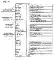
- Fig. 74 is another example of L1 signaling transmitted within a frame header.
- This Fig. 74 is different from Fig. 70 in that the L1_span field having 12 bits it is divided into two fields.
- the L1_span field is divided into a L1_colum having 9 bits and a L1_row having 3 bits.
- the L1_column represents the carrier index that L1 spans. Because data slice starts and ends at every 12 carriers, which is the pilot density, the 12 bits of overhead can be reduced by 3 bits to reach 9 bits.
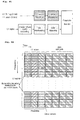
- Fig. 75 is an example of frequency or time interleaving/deinterleaving.
- the Fig. 75 shows a part of a whole transmission frame.
- the Fig. 75 also shows bonding of multiple 8 MHz bandwidths.
- a frame can consist of a preamble which transmits L1 blocks and a data symbol which transmits data.
- the different kinds of data symbols represent data slices for different services.
- the preamble transmits L1 blocks for every 7.61 MHz.
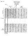
- frequency or time interleaving is performed within L1 blocks and not performed between L1 blocks. That is, for the preamble, it can be said that interleaving is performed at L1 block level. This allows decoding the L1 blocks by transmitting L1 blocks within a tuner window bandwidth even when the tuner window has moved to a random location within a channel bonding system.
- a symbol interleaver 308 in a data path of a BICM module of transmitter as shown in Fig. 37 can perform symbol interleaving for each data slice.
- a symbol interleaver 308-1 in an L1 signal path can perform symbol interleaving for each L1 block.
- a frequency interleaver 403 shown in Fig. 42 needs to perform interleaving on the preamble and data symbols separately. Specifically, for the preamble, frequency interleaving can be performed for each L1 block and for data symbol, frequency interleaving can be performed for each data slice. At this point, time interleaving in data path or L1 signal path may not be performed considering low latency mode.
- ACM/VCM type and multiple PLP cases frame can be kept same as for the FECFRAME header.
- the PLP identifier can be removed from the FECFRAME header, resulting in up to 1.8% overhead reduction.
- the Mod/Cod field can be removed from the FECFRAME header, resulting in up to 1.5% overhead reduction.
- no FECFRAME header is required, thus, up to 3.3% of overhead reduction can be obtained.
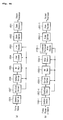
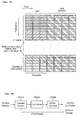
- Fig. 77 is showing a structure for a FECFRAME header for minimizing the overhead.
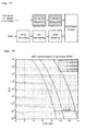
- the blocks with tilted lines and the FECFRAME Builder represent a detail block diagram of the ModCod Header Inserting module 307 on data path of the BICM module as shown in Fig. 37 .
- the solid blocks represent an example of inner coding module 303, inner interleaver 304, bit demux 305, and symbol mapper 306 on the data path of the BICM module as shown in Fig. 37 .
- shortened L1 signaling can be performed because CCM does not require a Mod/Cod field and single PLP does not require a PLP identifier.
- the LI signal can be repeated three times in the preamble and BPSK modulation can be performed, thus, a very robust signaling is possible.
- the ModCod Header Inserting module 307 can insert the generated header into each FEC frame.
- Fig. 84 is showing an example of the ModCod extracting module r307 on the data path of BICM demod module shown in Fig. 64 .
- the fecframe structure can be divided into two groups, in which the first group is the upper three frame structures with header and the second group is the last frame structure without header.
- Fig. 80 is showing an example of L1 signaling which can be transmitted within the preamble by the Frame header inserting module 401 of the Frame builder module shown in Fig. 42 .
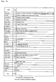
- This L1 signaling is different from the previous L1 signaling in that L1 block size can be transmitted in bits (L1_size, 14 bits); turning on/off time interleaving on data slice is possible (dslice_time_intrlv, 1 bit); and by defining data slice type (dslice_type, 1 bit), L1 signaling overhead is reduced.
- the shortened/punctured inner decoder r303-1 of the BICM demod as shown in Fig. 64 can obtain the first LDPC block, which has a fixed L1 block size, transmitted within the preamble, through decoding.
- the numbers and size of the rest of the LDPC blocks can also be obtained.
- Time interleaving can be used when multiple OFDM symbols are needed for L1 transmission or when there is a time-interleaved data slice.
- a flexible on/off of the time interleaving is possible with an interleaving flag.
- a time interleaving flag (1 bit) and a number of OFDM symbols interleaved (3 bits) may be required, thus, a total of 4 bits can be protected by a way similar to a shortened FECFRAME header.
- Fig. 81 is showing an example of L1-pre signaling that can be performed at the ModCod Header Inserting module 307-1 on the data path of BICM module shown in Fig. 37 .
- the blocks with tilted lines and Preamble Builder are examples of the ModCod Header Inserting module 307-1 on the L1 signaling path of the BICM module shown in Fig. 37 .
- the solid blocks are examples of the Frame header inserting module 401 of the Frame builder as shown in Fig. 42 .
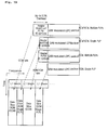
- Fig. 82 shows a structure of L1 the signaling block that is transmitted from the Frame header inserting module 401 of the Frame builder module as shown in Fig. 42 . It is showing a case where no time interleaving is used in a preamble.
- different kind of LDPC blocks can be transmitted in the order of the carriers. Once an OFDM symbol is formed and transmitted then a following OFDM symbol is formed and transmitted. For the last OFDM symbol to be transmitted, if there is any carrier left, that carriers can be used for data transmission or can be dummy padded.
- the example in Fig. 82 shows a preamble that comprises three OFDM symbol.
- the symbol deinterleaver r308-1 on the L1 signaling path of BICM demodulator as shown in Fig. 64 can be skipped.
- Fig. 83 shows a case where L1 time interleaving is performed.
- block interleaving can be performed in a fashion of forming an OFDM symbol for identical carrier indices then forming an OFDM symbols for the next carrier indices.
- no interleaving if there is any carrier left, that carriers can be used for data transmission or can be dummy padded.
- the symbol deinterleaver r308-1 on the L1 signaling path of the BICM demodulator shown in Fig. 64 can perform block deinterleaving by reading LDPC blocks in increasing order of numbers of the LDPC blocks.
- XFECFrame means XFEC(compleX Forward Error Correction)Frame and mod/cod means modulation type/coderate.
- a frame parser can form a frame from demodulated signals.
- the frame has data symbols and the data symbols can have a first type of data slice which has an XFECFrame and an XFECFrame header and a second type of data slice which has XFECFrame without XFECFrame header.
- a receiver can extract a field for indicating whether to perform time de-interleaving on the preamble symbols or not to perform time de-interleaving on the preamble symbols, from the L1 of the preamble symbols.
- Fig. 85 is showing another example of L1-pre signaling that can be transmitted from ModCod Header Inserting module 307-1 on L1 signalinig path of BICM module shown in Fig. 37 .
- Fig. 85 is different from Fig. 81 in that Header part protection mechanism has been modified.
- L1 block size information L1_size (14 bits) is not transmitted in L1 block, but transmitted in Header.
- time interleaving information of 4 bits can be transmitted too.
- BCH (45, 18) code which outputs 45 bits are used and copied to the two paths and finally, QPSK mapped.
- time interleaving depth is set as a number of preambles that is required to transmit L1 block, L1_span (3bits) that indicates time interleaving depth may not need to be transmitted. In other words, only time interleaving on/off flag (1 bit) can be transmitted.
- time deinterleaving depth can be obtained.
- Fig. 86 is showing an example of scheduling of L1 signaling block that is transmitted in preamble. If a size of L1 information that can be transmitted in a preamble is Nmax, when L1 size is smaller than Nmax, one preamble can transmit the information. However, when L1 size is bigger than Nmax, L1 information can be equally divided such that the divided L1 sub-block is smaller than Nmax, then the divided L1 sub-block can be transmitted in a preamble. At this point, for a carrier that is not used because of L1 information being smaller than Nmax, no data are transmitted.
- power of carriers where L1 block are transmitted can be boosted up to maintain a total preamble signal power equal to data symbol power.
- Power boosting factor can be varied depending on transmitted L1 size and a transmitter and a receiver can have a set value of this power boosting factor. For example, if only a half of total carriers are used, power boosting factor can be two.
- Fig. 87 is showing an example of L1-pre signaling where power boosting is considered. When compared to Fig. 85 , it can be seen that power of QPSK symbol can be boosted and sent to preamble builder.
- QPSK demapping can be performed and Log-Likelihood Ratio (LLR) value can be obtained.
- LLR Log-Likelihood Ratio
- PRBS demodulation according to sync word can be performed and a reverse process of the 1-bit cyclic shift can be performed for restoration.
- Output of hard decision can be input into BCH decoder.
- the BCH decoder can restore 18 bits of L1-pre from the input 45 bits.
- Fig. 90 is showing a counterpart, ModCod extractor of a receiver.
- power control can be performed on QPSK demapper input symbols to restore from power level boosted by transmitter to its original value.
- power control can be performed by considering a number of carriers used for L1 signaling in a preamble and by taking an inverse of obtained power boosting factor of a transmitter.
- the power boosting factor sets preamble power and data symbol power identical to each other.
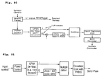
- Fig. 91 is showing an example of L1-pre synchronization that can be performed at ModCod extracting module r307-1 on L1 signaling path of BICM demod module shown in Fig. 64 .
- This is a synchronizing process to obtain a start position of Header in a preamble.
- Input symbols can be QPSK demapped then for the output Q-path, an inverse of 1 bit cyclic shift can be performed and alignment can be performed.
- Two I/Q paths values can be multiplied and modulated values by L1-pre signaling can be demodulated.
- output of multiplier can express only PRBS which is a sync word.
- PRBS which is a sync word.
- a correlation peak at Header can be obtained.
- a start position of Header in a preamble can be obtained.
- power control which is performed to restore original power level, as shown in Fig. 90 , can be performed on input of QPSK demapper.
- Fig. 92 is showing another example of L1 block header field which is sent to the Header Inserting module 307-1 on the L1 signaling path of the BICM module as shown in Fig. 37 .
- This Fig. 92 is different from Fig. 85 in that L1 span which represents the time interleaving depth is reduced to 2 bits and reserved bits are increased by 1 bit.
- a receiver can obtain time interleaving parameter of L1 block from the transmitted L1_span
- Fig. 93 is showing processes of equally dividing a L1 block into as many portions as a number of preambles then inserting a header into each of the divided L1 blocks and then assigning the header inserted L1 blocks into a preamble. This can be performed when a time interleaving is performed with a number of preambles where the number of preambles is greater than a minimum number of preambles that is required for transmitting L1 block. This can be performed at the L1 block on the L1 signaling path of the BICM module as shown in Fig. 37 . The rest of the carriers, after transmitting L1 blocks can have cyclic repetition patterns instead of being zero padded.
- only the repeated part can be divided into as many as a number of FEC block header and the other part can be divided by a value which is one less than a number of FEC block header.
- the dividing number corresponds to a number of carriers that is added to each carrier.
- ModCod information in each BB frame header that is necessary for ACM/VCM By transmitting ModCod information in each BB frame header that is necessary for ACM/VCM and transmitting the rest of the physical layer signaling in a frame header, signaling overhead can be minimized.
- Modified QAM for a more energy efficient transmission or a more noise-robust digital broadcasting system can be implemented.
- the system can include transmitter and receiver for each example disclosed and the combinations thereof.
- An Improved Non-uniform QAM for a more energy efficient transmission or a more noise-robust digital broadcasting system can be implemented.
- a method of using code rate of error correction code of NU-MQAM and MQAM is also described.
- the system can include transmitter and receiver for each example disclosed and the combinations thereof.
- the suggested L1 signaling method can reduce overhead by 3 ⁇ 4% by minimizing signaling overhead during channel bonding.
Landscapes
- Engineering & Computer Science (AREA)
- Signal Processing (AREA)
- Computer Networks & Wireless Communication (AREA)
- Error Detection And Correction (AREA)
- Radar Systems Or Details Thereof (AREA)
- Digital Transmission Methods That Use Modulated Carrier Waves (AREA)
- Time-Division Multiplex Systems (AREA)
Claims (14)
- Verfahren zum Senden eines Rundrufsignals an einen Empfänger, wobei das Verfahren aufweist:Codieren von Daten des Kanals der physikalischen Schicht (PLP) zum Befördern wenigstens eines Dienstes und von Schicht-1- (L1-) Signalisierungsdaten zur Signalisierung der PLP-Daten;dadurch gekennzeichnet, dass es ferner aufweist:Zeitverschachteln der codierten L1-Signalisierungsdaten und Ausgeben eines Schicht-1- (L1-) TI-Blocks basierend auf L1-TI-Modusinformationen;Einfügen eines Schicht-1- (L1-) Anfangsblocks vor dem L1-TI-Block, um einen Schicht-1- (L1-) Block aufzubauen, wobei der L1-T1-Block mit dem L1-Anfangsblock innerhalb des L1-Blocks in der Frequenzdomäne wiederholt wird;Aufbauen eines Signalrahmens einschließlich von Präambelsymbolen und Symbolen der codierten PLP-Daten, wobei die Präambelsymbole in L1-Blöcke mit der gleichen Bandbreite aufgeteilt werden;Modulieren des Signalrahmens durch ein orthogonales Frequenzteilungsmultiplex- (OFDM-) Verfahren; undSenden des modulierten Signalrahmens.
- Verfahren nach Anspruch 1, wobei der L1-Anfangsblock L1-TI-Modusinformationen hat, die den Modus der Zeitverschachtelung für die Präambelsymbole angeben.
- Verfahren nach Anspruch 1 oder 2, wobei eine Bandbreite des L1-Blocks entweder 7,61 MHz oder 8 MHz ist.
- Verfahren zum Empfangen eines Rundrufsignals, wobei das Verfahren aufweist:Demodulieren des empfangenen Signals unter Verwendung eines orthogonalen Frequenzteilungsmultiplex- (OFDM-) Verfahrens,dadurch gekennzeichnet, dass es ferner aufweist:Gewinnen eines Signalrahmens aus den demodulierten Signalen, wobei der Signalrahmen Präambelsymbole und Datensymbole des Kanals der physikalischen Schicht (PLP) aufweist, wobei die Präambelsymbole in Schicht-1- (L1-) Blöcke mit der gleichen Bandbreite aufgeteilt werden, wobei wenigstens ein L1-TI-Block mit einem L1-Anfangsblock innerhalb des L1-Blocks in der Frequenzdomäne wiederholt wird; wobei der L1-TI-Block L1-Signalisierungsdaten zur Signalisierung der Datensymbole hat;Zeitentschachteln der L1-Signalisierungsdaten des L1-TI-Blocks basierend auf L1-TI-Modusinformationen; undDecodieren der zeitverschachtelten L1-Signalisierungsdaten.
- Verfahren nach Anspruch 4, wobei der L1-Anfangsblock die L1-TI-Modusinformationen hat, die den Modus der Zeitentschachtelung für L1-Signalisierungsinformationen angeben.
- Verfahren nach Anspruch 4 oder 5, wobei eine Bandbreite des L1-Blocks entweder 7,61 MHz oder 8 MHz ist.
- Verfahren nach Anspruch 5,
wobei das Decodieren durch ein verkürztes und punktiertes LDPC-Schema durchgeführt wird. - Sender zum Senden eines Rundrufsignals an einen Empfänger, wobei der Sender aufweist:Einrichtungen (102) zum Codieren von Daten des Kanals der physikalischen Schicht (PLP) zum Befördern wenigstens eines Dienstes und von Schicht-1- (L1-) Signalisierungsdaten zur Signalisierung der PLP-Daten;dadurch gekennzeichnet, dass er ferner aufweist:Einrichtungen (308-1) zum Zeitverschachteln der codierten L1-Signalisierungsdaten und Ausgeben eines Schicht-1- (L1-) TI-Blocks basierend auf L1-TI-Modusinformationen;Einrichtungen (103) zum Einfügen eines Schicht-1-(L1-) Anfangsblocks vor dem L1-TI-Block, um einen Schicht-1-(L1-) Block aufzubauen, wobei der L1-TI-Block mit dem L1-Anfangsblock innerhalb des L1-Blocks in der Frequenzdomäne wiederholt wird;Einrichtungen (103) zum Aufbauen eines Signalrahmens einschließlich von Präambelsymbolen und Symbolen der codierten PLP-Daten, wobei die Präambelsymbole in L1-Blöcke mit der gleichen Bandbreite aufgeteilt werden;Einrichtungen (104) zum Modulieren des Signalrahmens durch ein orthogonales Frequenzteilungsmultiplex- (OFDM-) Verfahren; undEinrichtungen (105) zum Senden des modulierten Signalrahmens.
- Sender nach Anspruch 8, wobei der L1-Anfangsblock L1-TI-Modusinformationen hat, die den Modus der Zeitverschachtelung für die Präambelsymbole angeben.
- Sender nach Anspruch 8 oder 9, wobei eine Bandbreite des L1-Blocks entweder 7,61 MHz oder 8 MHz ist.
- Empfänger zum Empfangen eines Rundrufsignals, wobei der Empfänger aufweist:Einrichtungen (r104) zum Demodulieren des empfangenen Signals unter Verwendung eines orthogonalen Frequenzteilungsmultiplex- (OFDM-) Verfahrens,dadurch gekennzeichnet, dass es ferner aufweist:Einrichtungen (r103) zum Gewinnen eines Signalrahmens aus den demodulierten Signalen, wobei der Signalrahmen Präambelsymbole und Datensymbole des Kanals der physikalischen Schicht (PLP) aufweist, wobei die Präambelsymbole in Schicht-1- (L1-) Blöcke mit der gleichen Bandbreite aufgeteilt werden, wobei wenigstens ein L1-TI-Block mit einem L1-Anfangsblock innerhalb des L1-Blocks in der Frequenzdomäne wiederholt wird; wobei der L1-TI-Block L1-Signalisierungsdaten zur Signalisierung der Datensymbole hat;Einrichtungen (r308-1) zum Zeitentschachteln der L1-Signalisierungsdaten des L1-TI-Blocks basierend auf L1-TI-Modusinformationen; undEinrichtungen (r306-1) zum Decodieren der zeitverschachtelten L1-Signalisierungsdaten.
- Empfänger nach Anspruch 11, wobei der L1-Anfangsblock die L1-TI-Modusinformationen hat, die den Modus der Zeitentschachtelung für L1-Signalisierungsinformationen angeben.
- Empfänger nach Anspruch 11, wobei eine Bandbreite des L1-Blocks entweder 7,61 MHz oder 8 MHz ist.
- Empfänger nach Anspruch 11,
wobei das Decodieren durch ein verkürztes und punktiertes LDPC-Schema durchgeführt wird.
Priority Applications (7)
| Application Number | Priority Date | Filing Date | Title |
|---|---|---|---|
| EP11162356A EP2357747B1 (de) | 2008-11-16 | 2009-06-03 | Vorrichtung zum Senden und Empfangen eines Signals und Verfahren zum Senden und Empfangen eines Signals |
| EP11162353A EP2381598B1 (de) | 2008-11-16 | 2009-06-03 | Vorrichtung zum Senden und Empfangen eines Signals und Verfahren zum Senden und Empfangen eines Signals |
| PL11162353T PL2381598T3 (pl) | 2008-11-16 | 2009-06-03 | Urządzenie do nadawania i odbierania sygnału oraz sposób nadawania i odbierania sygnału |
| SI200930102T SI2187543T1 (sl) | 2008-11-16 | 2009-06-03 | Naprava za oddajanje in sprejemanje signala ter postopek oddajanja in sprejemanja signala |
| PL09161830T PL2187543T3 (pl) | 2008-11-16 | 2009-06-03 | Urządzenie do nadawania i odbierania sygnału oraz sposób nadawania i odbierania sygnału |
| DK11162356.7T DK2357747T3 (da) | 2008-11-16 | 2009-06-03 | Apparat til at sende og modtage et signal og fremgangsmåde til at sende og modtage et signal |
| PL11162356T PL2357747T3 (pl) | 2008-11-16 | 2009-06-03 | Urządzenie do nadawania i odbierania sygnału oraz sposób nadawania i odbierania sygnału |
Applications Claiming Priority (1)
| Application Number | Priority Date | Filing Date | Title |
|---|---|---|---|
| US11510308P | 2008-11-16 | 2008-11-16 |
Related Child Applications (4)
| Application Number | Title | Priority Date | Filing Date |
|---|---|---|---|
| EP11162353A Division EP2381598B1 (de) | 2008-11-16 | 2009-06-03 | Vorrichtung zum Senden und Empfangen eines Signals und Verfahren zum Senden und Empfangen eines Signals |
| EP11162356A Division EP2357747B1 (de) | 2008-11-16 | 2009-06-03 | Vorrichtung zum Senden und Empfangen eines Signals und Verfahren zum Senden und Empfangen eines Signals |
| EP11162356.7 Division-Into | 2011-04-14 | ||
| EP11162353.4 Division-Into | 2011-04-14 |
Publications (2)
| Publication Number | Publication Date |
|---|---|
| EP2187543A1 EP2187543A1 (de) | 2010-05-19 |
| EP2187543B1 true EP2187543B1 (de) | 2011-08-10 |
Family
ID=41232266
Family Applications (3)
| Application Number | Title | Priority Date | Filing Date |
|---|---|---|---|
| EP09161830A Active EP2187543B1 (de) | 2008-11-16 | 2009-06-03 | Vorrichtung zum Senden und Empfangen eines Signals und Verfahren zum Senden und Empfangen eines Signals |
| EP11162353A Not-in-force EP2381598B1 (de) | 2008-11-16 | 2009-06-03 | Vorrichtung zum Senden und Empfangen eines Signals und Verfahren zum Senden und Empfangen eines Signals |
| EP11162356A Not-in-force EP2357747B1 (de) | 2008-11-16 | 2009-06-03 | Vorrichtung zum Senden und Empfangen eines Signals und Verfahren zum Senden und Empfangen eines Signals |
Family Applications After (2)
| Application Number | Title | Priority Date | Filing Date |
|---|---|---|---|
| EP11162353A Not-in-force EP2381598B1 (de) | 2008-11-16 | 2009-06-03 | Vorrichtung zum Senden und Empfangen eines Signals und Verfahren zum Senden und Empfangen eines Signals |
| EP11162356A Not-in-force EP2357747B1 (de) | 2008-11-16 | 2009-06-03 | Vorrichtung zum Senden und Empfangen eines Signals und Verfahren zum Senden und Empfangen eines Signals |
Country Status (9)
| Country | Link |
|---|---|
| EP (3) | EP2187543B1 (de) |
| CN (1) | CN102217265B (de) |
| AT (1) | ATE520212T1 (de) |
| DK (2) | DK2357747T3 (de) |
| ES (3) | ES2395480T3 (de) |
| PL (3) | PL2381598T3 (de) |
| PT (3) | PT2187543E (de) |
| SI (3) | SI2187543T1 (de) |
| WO (1) | WO2010055981A1 (de) |
Families Citing this family (7)
| Publication number | Priority date | Publication date | Assignee | Title |
|---|---|---|---|---|
| WO2010071273A1 (en) * | 2008-12-21 | 2010-06-24 | Lg Electronics Inc. | Apparatus for transmitting and receiving a signal and method of transmitting and receiving a signal |
| KR101658555B1 (ko) | 2013-01-17 | 2016-09-21 | 엘지전자 주식회사 | 방송 신호 송신 장치, 방송 신호 수신 장치, 방송 신호 송신 방법 및 방송 신호 수신 방법 |
| CN103986678B (zh) * | 2013-02-11 | 2017-12-26 | 芯迪半导体科技(上海)有限公司 | 一种用于正交频分复用ofdm信道估计的接收机及其估计方法 |
| CN105493498B (zh) | 2013-08-23 | 2018-12-04 | Lg 电子株式会社 | 发送广播信号的方法及装置、接收广播信号的方法及装置 |
| CN105991227B (zh) * | 2015-02-15 | 2020-03-03 | 中兴通讯股份有限公司 | 数据编码方法及装置 |
| EP3284192B1 (de) * | 2015-04-14 | 2019-12-04 | Sony Corporation | Codierungs- und modulationsvorrichtung mit verwendung von ungleichförmiger konstellation und unterschiedlichen phy-modi |
| CN107950029B (zh) * | 2015-09-10 | 2020-07-03 | Lg 电子株式会社 | 广播信号发送装置和方法以及广播信号接收装置和方法 |
Family Cites Families (3)
| Publication number | Priority date | Publication date | Assignee | Title |
|---|---|---|---|---|
| FI108822B (fi) * | 2000-02-14 | 2002-03-28 | Nokia Corp | Lomittelumenetelmä ja -järjestelmä |
| EP2122833A2 (de) * | 2007-01-16 | 2009-11-25 | Koninklijke Philips Electronics N.V. | System, vorrichtung und verfahren zur verschachtelung von datenbits oder -symbolen |
| KR100921465B1 (ko) * | 2007-04-19 | 2009-10-13 | 엘지전자 주식회사 | 디지털 방송 신호 송수신기 및 그 제어 방법 |
-
2009
- 2009-05-13 CN CN200980145372.0A patent/CN102217265B/zh not_active Expired - Fee Related
- 2009-05-13 WO PCT/KR2009/002546 patent/WO2010055981A1/en not_active Ceased
- 2009-06-03 ES ES11162353T patent/ES2395480T3/es active Active
- 2009-06-03 ES ES09161830T patent/ES2371388T3/es active Active
- 2009-06-03 DK DK11162356.7T patent/DK2357747T3/da active
- 2009-06-03 PT PT09161830T patent/PT2187543E/pt unknown
- 2009-06-03 SI SI200930102T patent/SI2187543T1/sl unknown
- 2009-06-03 SI SI200930407T patent/SI2381598T1/sl unknown
- 2009-06-03 EP EP09161830A patent/EP2187543B1/de active Active
- 2009-06-03 PL PL11162353T patent/PL2381598T3/pl unknown
- 2009-06-03 DK DK09161830.6T patent/DK2187543T3/da active
- 2009-06-03 SI SI200930446T patent/SI2357747T1/sl unknown
- 2009-06-03 PL PL09161830T patent/PL2187543T3/pl unknown
- 2009-06-03 PL PL11162356T patent/PL2357747T3/pl unknown
- 2009-06-03 PT PT111623567T patent/PT2357747E/pt unknown
- 2009-06-03 EP EP11162353A patent/EP2381598B1/de not_active Not-in-force
- 2009-06-03 EP EP11162356A patent/EP2357747B1/de not_active Not-in-force
- 2009-06-03 ES ES11162356T patent/ES2395711T3/es active Active
- 2009-06-03 AT AT09161830T patent/ATE520212T1/de not_active IP Right Cessation
- 2009-06-03 PT PT111623534T patent/PT2381598E/pt unknown
Also Published As
| Publication number | Publication date |
|---|---|
| EP2187543A1 (de) | 2010-05-19 |
| DK2357747T3 (da) | 2013-01-07 |
| PT2381598E (pt) | 2012-12-10 |
| SI2357747T1 (sl) | 2013-02-28 |
| SI2381598T1 (sl) | 2013-02-28 |
| EP2357747B1 (de) | 2012-09-19 |
| ATE520212T1 (de) | 2011-08-15 |
| PL2357747T3 (pl) | 2013-02-28 |
| EP2381598A1 (de) | 2011-10-26 |
| EP2381598B1 (de) | 2012-09-05 |
| SI2187543T1 (sl) | 2011-12-30 |
| CN102217265B (zh) | 2014-05-28 |
| PL2187543T3 (pl) | 2011-12-30 |
| ES2371388T3 (es) | 2011-12-30 |
| PL2381598T3 (pl) | 2013-02-28 |
| ES2395480T3 (es) | 2013-02-13 |
| EP2357747A1 (de) | 2011-08-17 |
| DK2187543T3 (da) | 2011-12-05 |
| CN102217265A (zh) | 2011-10-12 |
| ES2395711T3 (es) | 2013-02-14 |
| PT2357747E (pt) | 2012-12-24 |
| PT2187543E (pt) | 2011-11-22 |
| WO2010055981A1 (en) | 2010-05-20 |
Similar Documents
| Publication | Publication Date | Title |
|---|---|---|
| EP2323330B1 (de) | Vorrichtung und verfahren zum senden und empfangen eines signals | |
| EP2182669A1 (de) | Vorrichtung und Verfahren zum Senden und Empfangen eines Rundfunksignals | |
| EP2432145B1 (de) | Vorrichtung zum Senden und Empfangen eines Signals und Verfahren zum Senden und Empfangen eines Signals | |
| EP2677678B1 (de) | Vorrichtung und Methode zum Senden und Empfangen eines Rundfunksignals | |
| EP2385668B1 (de) | Vorrichtung zum Senden und Empfangen eines Signals und Verfahren zum Senden und Empfangen eines Signals | |
| EP2200196B1 (de) | Vorrichtung zum Senden und Empfangen eines Signals und Verfahren zum Senden und Empfangen eines Signals | |
| EP2357747B1 (de) | Vorrichtung zum Senden und Empfangen eines Signals und Verfahren zum Senden und Empfangen eines Signals | |
| EP2434678B1 (de) | Vorrichtung zum Senden und Empfangen eines Signals und Verfahren zum Senden und Empfangen eines Signals | |
| EP2187556B1 (de) | Vorrichtung und Verfahren zum Senden und Empfangen eines Rundfunksignals | |
| EP2200206A2 (de) | Vorrichtung und Methode zum Senden und Empfangen eines Rundfunksignals | |
| EP2197137A2 (de) | Vorrichtung und Methode zum Senden und Empfangen eines Rundfunksignals |
Legal Events
| Date | Code | Title | Description |
|---|---|---|---|
| PUAI | Public reference made under article 153(3) epc to a published international application that has entered the european phase |
Free format text: ORIGINAL CODE: 0009012 |
|
| 17P | Request for examination filed |
Effective date: 20090603 |
|
| AK | Designated contracting states |
Kind code of ref document: A1 Designated state(s): AT BE BG CH CY CZ DE DK EE ES FI FR GB GR HR HU IE IS IT LI LT LU LV MC MK MT NL NO PL PT RO SE SI SK TR |
|
| 17Q | First examination report despatched |
Effective date: 20100506 |
|
| GRAP | Despatch of communication of intention to grant a patent |
Free format text: ORIGINAL CODE: EPIDOSNIGR1 |
|
| RIC1 | Information provided on ipc code assigned before grant |
Ipc: H04L 1/00 20060101ALI20110120BHEP Ipc: H04L 5/00 20060101ALI20110120BHEP Ipc: H04L 27/34 20060101ALI20110120BHEP Ipc: H04L 27/26 20060101ALI20110120BHEP Ipc: H04H 20/76 20080101ALI20110120BHEP Ipc: H03M 13/00 20060101ALI20110120BHEP Ipc: H04H 20/65 20080101AFI20110120BHEP |
|
| GRAS | Grant fee paid |
Free format text: ORIGINAL CODE: EPIDOSNIGR3 |
|
| GRAA | (expected) grant |
Free format text: ORIGINAL CODE: 0009210 |
|
| AK | Designated contracting states |
Kind code of ref document: B1 Designated state(s): AT BE BG CH CY CZ DE DK EE ES FI FR GB GR HR HU IE IS IT LI LT LU LV MC MK MT NL NO PL PT RO SE SI SK TR |
|
| REG | Reference to a national code |
Ref country code: GB Ref legal event code: FG4D |
|
| REG | Reference to a national code |
Ref country code: CH Ref legal event code: EP |
|
| REG | Reference to a national code |
Ref country code: IE Ref legal event code: FG4D |
|
| REG | Reference to a national code |
Ref country code: DE Ref legal event code: R096 Ref document number: 602009002054 Country of ref document: DE Effective date: 20111020 |
|
| REG | Reference to a national code |
Ref country code: PT Ref legal event code: SC4A Free format text: AVAILABILITY OF NATIONAL TRANSLATION Effective date: 20111107 |
|
| REG | Reference to a national code |
Ref country code: SE Ref legal event code: TRGR |
|
| REG | Reference to a national code |
Ref country code: NL Ref legal event code: T3 |
|
| REG | Reference to a national code |
Ref country code: DK Ref legal event code: T3 |
|
| REG | Reference to a national code |
Ref country code: PL Ref legal event code: T3 Ref country code: ES Ref legal event code: FG2A Ref document number: 2371388 Country of ref document: ES Kind code of ref document: T3 Effective date: 20111230 |
|
| REG | Reference to a national code |
Ref country code: SK Ref legal event code: T3 Ref document number: E 10419 Country of ref document: SK |
|
| LTIE | Lt: invalidation of european patent or patent extension |
Effective date: 20110810 |
|
| PG25 | Lapsed in a contracting state [announced via postgrant information from national office to epo] |
Ref country code: IS Free format text: LAPSE BECAUSE OF FAILURE TO SUBMIT A TRANSLATION OF THE DESCRIPTION OR TO PAY THE FEE WITHIN THE PRESCRIBED TIME-LIMIT Effective date: 20111210 Ref country code: FI Free format text: LAPSE BECAUSE OF FAILURE TO SUBMIT A TRANSLATION OF THE DESCRIPTION OR TO PAY THE FEE WITHIN THE PRESCRIBED TIME-LIMIT Effective date: 20110810 Ref country code: LT Free format text: LAPSE BECAUSE OF FAILURE TO SUBMIT A TRANSLATION OF THE DESCRIPTION OR TO PAY THE FEE WITHIN THE PRESCRIBED TIME-LIMIT Effective date: 20110810 Ref country code: HR Free format text: LAPSE BECAUSE OF FAILURE TO SUBMIT A TRANSLATION OF THE DESCRIPTION OR TO PAY THE FEE WITHIN THE PRESCRIBED TIME-LIMIT Effective date: 20110810 Ref country code: NO Free format text: LAPSE BECAUSE OF FAILURE TO SUBMIT A TRANSLATION OF THE DESCRIPTION OR TO PAY THE FEE WITHIN THE PRESCRIBED TIME-LIMIT Effective date: 20111110 |
|
| REG | Reference to a national code |
Ref country code: AT Ref legal event code: MK05 Ref document number: 520212 Country of ref document: AT Kind code of ref document: T Effective date: 20110810 |
|
| PG25 | Lapsed in a contracting state [announced via postgrant information from national office to epo] |
Ref country code: GR Free format text: LAPSE BECAUSE OF FAILURE TO SUBMIT A TRANSLATION OF THE DESCRIPTION OR TO PAY THE FEE WITHIN THE PRESCRIBED TIME-LIMIT Effective date: 20111111 Ref country code: AT Free format text: LAPSE BECAUSE OF FAILURE TO SUBMIT A TRANSLATION OF THE DESCRIPTION OR TO PAY THE FEE WITHIN THE PRESCRIBED TIME-LIMIT Effective date: 20110810 Ref country code: CY Free format text: LAPSE BECAUSE OF FAILURE TO SUBMIT A TRANSLATION OF THE DESCRIPTION OR TO PAY THE FEE WITHIN THE PRESCRIBED TIME-LIMIT Effective date: 20110810 Ref country code: LV Free format text: LAPSE BECAUSE OF FAILURE TO SUBMIT A TRANSLATION OF THE DESCRIPTION OR TO PAY THE FEE WITHIN THE PRESCRIBED TIME-LIMIT Effective date: 20110810 |
|
| PG25 | Lapsed in a contracting state [announced via postgrant information from national office to epo] |
Ref country code: BE Free format text: LAPSE BECAUSE OF FAILURE TO SUBMIT A TRANSLATION OF THE DESCRIPTION OR TO PAY THE FEE WITHIN THE PRESCRIBED TIME-LIMIT Effective date: 20110810 |
|
| PG25 | Lapsed in a contracting state [announced via postgrant information from national office to epo] |
Ref country code: CZ Free format text: LAPSE BECAUSE OF FAILURE TO SUBMIT A TRANSLATION OF THE DESCRIPTION OR TO PAY THE FEE WITHIN THE PRESCRIBED TIME-LIMIT Effective date: 20110810 |
|
| REG | Reference to a national code |
Ref country code: HU Ref legal event code: AG4A Ref document number: E012769 Country of ref document: HU |
|
| PG25 | Lapsed in a contracting state [announced via postgrant information from national office to epo] |
Ref country code: EE Free format text: LAPSE BECAUSE OF FAILURE TO SUBMIT A TRANSLATION OF THE DESCRIPTION OR TO PAY THE FEE WITHIN THE PRESCRIBED TIME-LIMIT Effective date: 20110810 Ref country code: RO Free format text: LAPSE BECAUSE OF FAILURE TO SUBMIT A TRANSLATION OF THE DESCRIPTION OR TO PAY THE FEE WITHIN THE PRESCRIBED TIME-LIMIT Effective date: 20110810 |
|
| PLBE | No opposition filed within time limit |
Free format text: ORIGINAL CODE: 0009261 |
|
| STAA | Information on the status of an ep patent application or granted ep patent |
Free format text: STATUS: NO OPPOSITION FILED WITHIN TIME LIMIT |
|
| 26N | No opposition filed |
Effective date: 20120511 |
|
| REG | Reference to a national code |
Ref country code: DE Ref legal event code: R097 Ref document number: 602009002054 Country of ref document: DE Effective date: 20120511 |
|
| PG25 | Lapsed in a contracting state [announced via postgrant information from national office to epo] |
Ref country code: MC Free format text: LAPSE BECAUSE OF NON-PAYMENT OF DUE FEES Effective date: 20120630 |
|
| PG25 | Lapsed in a contracting state [announced via postgrant information from national office to epo] |
Ref country code: MK Free format text: LAPSE BECAUSE OF FAILURE TO SUBMIT A TRANSLATION OF THE DESCRIPTION OR TO PAY THE FEE WITHIN THE PRESCRIBED TIME-LIMIT Effective date: 20110810 |
|
| REG | Reference to a national code |
Ref country code: IE Ref legal event code: MM4A |
|
| PG25 | Lapsed in a contracting state [announced via postgrant information from national office to epo] |
Ref country code: IE Free format text: LAPSE BECAUSE OF NON-PAYMENT OF DUE FEES Effective date: 20120603 |
|
| PG25 | Lapsed in a contracting state [announced via postgrant information from national office to epo] |
Ref country code: BG Free format text: LAPSE BECAUSE OF FAILURE TO SUBMIT A TRANSLATION OF THE DESCRIPTION OR TO PAY THE FEE WITHIN THE PRESCRIBED TIME-LIMIT Effective date: 20111110 |
|
| PG25 | Lapsed in a contracting state [announced via postgrant information from national office to epo] |
Ref country code: MT Free format text: LAPSE BECAUSE OF FAILURE TO SUBMIT A TRANSLATION OF THE DESCRIPTION OR TO PAY THE FEE WITHIN THE PRESCRIBED TIME-LIMIT Effective date: 20110810 |
|
| REG | Reference to a national code |
Ref country code: CH Ref legal event code: PL |
|
| PG25 | Lapsed in a contracting state [announced via postgrant information from national office to epo] |
Ref country code: TR Free format text: LAPSE BECAUSE OF FAILURE TO SUBMIT A TRANSLATION OF THE DESCRIPTION OR TO PAY THE FEE WITHIN THE PRESCRIBED TIME-LIMIT Effective date: 20110810 Ref country code: LI Free format text: LAPSE BECAUSE OF NON-PAYMENT OF DUE FEES Effective date: 20130630 Ref country code: CH Free format text: LAPSE BECAUSE OF NON-PAYMENT OF DUE FEES Effective date: 20130630 |
|
| PG25 | Lapsed in a contracting state [announced via postgrant information from national office to epo] |
Ref country code: LU Free format text: LAPSE BECAUSE OF NON-PAYMENT OF DUE FEES Effective date: 20120603 |
|
| REG | Reference to a national code |
Ref country code: FR Ref legal event code: PLFP Year of fee payment: 7 |
|
| REG | Reference to a national code |
Ref country code: FR Ref legal event code: PLFP Year of fee payment: 8 |
|
| REG | Reference to a national code |
Ref country code: FR Ref legal event code: PLFP Year of fee payment: 9 |
|
| REG | Reference to a national code |
Ref country code: FR Ref legal event code: PLFP Year of fee payment: 10 |
|
| PGFP | Annual fee paid to national office [announced via postgrant information from national office to epo] |
Ref country code: PT Payment date: 20200507 Year of fee payment: 12 Ref country code: DK Payment date: 20200507 Year of fee payment: 12 Ref country code: NL Payment date: 20200507 Year of fee payment: 12 |
|
| PGFP | Annual fee paid to national office [announced via postgrant information from national office to epo] |
Ref country code: SE Payment date: 20200507 Year of fee payment: 12 Ref country code: HU Payment date: 20200602 Year of fee payment: 12 Ref country code: SK Payment date: 20200511 Year of fee payment: 12 Ref country code: PL Payment date: 20200508 Year of fee payment: 12 Ref country code: IT Payment date: 20200619 Year of fee payment: 12 Ref country code: SI Payment date: 20200514 Year of fee payment: 12 |
|
| PGFP | Annual fee paid to national office [announced via postgrant information from national office to epo] |
Ref country code: ES Payment date: 20200709 Year of fee payment: 12 |
|
| REG | Reference to a national code |
Ref country code: DK Ref legal event code: EBP Effective date: 20210630 |
|
| REG | Reference to a national code |
Ref country code: SE Ref legal event code: EUG |
|
| PG25 | Lapsed in a contracting state [announced via postgrant information from national office to epo] |
Ref country code: PT Free format text: LAPSE BECAUSE OF NON-PAYMENT OF DUE FEES Effective date: 20211203 |
|
| REG | Reference to a national code |
Ref country code: NL Ref legal event code: MM Effective date: 20210701 |
|
| REG | Reference to a national code |
Ref country code: SK Ref legal event code: MM4A Ref document number: E 10419 Country of ref document: SK Effective date: 20210603 |
|
| PG25 | Lapsed in a contracting state [announced via postgrant information from national office to epo] |
Ref country code: SI Free format text: LAPSE BECAUSE OF NON-PAYMENT OF DUE FEES Effective date: 20210604 |
|
| REG | Reference to a national code |
Ref country code: SI Ref legal event code: KO00 Effective date: 20220125 |
|
| PG25 | Lapsed in a contracting state [announced via postgrant information from national office to epo] |
Ref country code: HU Free format text: LAPSE BECAUSE OF NON-PAYMENT OF DUE FEES Effective date: 20210604 |
|
| PG25 | Lapsed in a contracting state [announced via postgrant information from national office to epo] |
Ref country code: SK Free format text: LAPSE BECAUSE OF NON-PAYMENT OF DUE FEES Effective date: 20210603 Ref country code: SE Free format text: LAPSE BECAUSE OF NON-PAYMENT OF DUE FEES Effective date: 20210604 Ref country code: NL Free format text: LAPSE BECAUSE OF NON-PAYMENT OF DUE FEES Effective date: 20210701 |
|
| PG25 | Lapsed in a contracting state [announced via postgrant information from national office to epo] |
Ref country code: IT Free format text: LAPSE BECAUSE OF NON-PAYMENT OF DUE FEES Effective date: 20210603 Ref country code: DK Free format text: LAPSE BECAUSE OF NON-PAYMENT OF DUE FEES Effective date: 20210630 |
|
| REG | Reference to a national code |
Ref country code: ES Ref legal event code: FD2A Effective date: 20220826 |
|
| PG25 | Lapsed in a contracting state [announced via postgrant information from national office to epo] |
Ref country code: ES Free format text: LAPSE BECAUSE OF NON-PAYMENT OF DUE FEES Effective date: 20210604 |
|
| PG25 | Lapsed in a contracting state [announced via postgrant information from national office to epo] |
Ref country code: PL Free format text: LAPSE BECAUSE OF NON-PAYMENT OF DUE FEES Effective date: 20210603 |
|
| P01 | Opt-out of the competence of the unified patent court (upc) registered |
Effective date: 20230610 |
|
| PGFP | Annual fee paid to national office [announced via postgrant information from national office to epo] |
Ref country code: DE Payment date: 20250508 Year of fee payment: 17 |
|
| PGFP | Annual fee paid to national office [announced via postgrant information from national office to epo] |
Ref country code: GB Payment date: 20250508 Year of fee payment: 17 |
|
| PGFP | Annual fee paid to national office [announced via postgrant information from national office to epo] |
Ref country code: FR Payment date: 20250513 Year of fee payment: 17 |