EP2188406B1 - Procédé de fabrication d'un film composite - Google Patents
Procédé de fabrication d'un film composite Download PDFInfo
- Publication number
- EP2188406B1 EP2188406B1 EP07803444.4A EP07803444A EP2188406B1 EP 2188406 B1 EP2188406 B1 EP 2188406B1 EP 07803444 A EP07803444 A EP 07803444A EP 2188406 B1 EP2188406 B1 EP 2188406B1
- Authority
- EP
- European Patent Office
- Prior art keywords
- deposition
- substrate
- source
- compound film
- film
- Prior art date
- Legal status (The legal status is an assumption and is not a legal conclusion. Google has not performed a legal analysis and makes no representation as to the accuracy of the status listed.)
- Active
Links
Images



Classifications
-
- C—CHEMISTRY; METALLURGY
- C23—COATING METALLIC MATERIAL; COATING MATERIAL WITH METALLIC MATERIAL; CHEMICAL SURFACE TREATMENT; DIFFUSION TREATMENT OF METALLIC MATERIAL; COATING BY VACUUM EVAPORATION, BY SPUTTERING, BY ION IMPLANTATION OR BY CHEMICAL VAPOUR DEPOSITION, IN GENERAL; INHIBITING CORROSION OF METALLIC MATERIAL OR INCRUSTATION IN GENERAL
- C23C—COATING METALLIC MATERIAL; COATING MATERIAL WITH METALLIC MATERIAL; SURFACE TREATMENT OF METALLIC MATERIAL BY DIFFUSION INTO THE SURFACE, BY CHEMICAL CONVERSION OR SUBSTITUTION; COATING BY VACUUM EVAPORATION, BY SPUTTERING, BY ION IMPLANTATION OR BY CHEMICAL VAPOUR DEPOSITION, IN GENERAL
- C23C14/00—Coating by vacuum evaporation, by sputtering or by ion implantation of the coating forming material
- C23C14/06—Coating by vacuum evaporation, by sputtering or by ion implantation of the coating forming material characterised by the coating material
- C23C14/0623—Sulfides, selenides or tellurides
-
- H—ELECTRICITY
- H10—SEMICONDUCTOR DEVICES; ELECTRIC SOLID-STATE DEVICES NOT OTHERWISE PROVIDED FOR
- H10F—INORGANIC SEMICONDUCTOR DEVICES SENSITIVE TO INFRARED RADIATION, LIGHT, ELECTROMAGNETIC RADIATION OF SHORTER WAVELENGTH OR CORPUSCULAR RADIATION
- H10F71/00—Manufacture or treatment of devices covered by this subclass
-
- C—CHEMISTRY; METALLURGY
- C23—COATING METALLIC MATERIAL; COATING MATERIAL WITH METALLIC MATERIAL; CHEMICAL SURFACE TREATMENT; DIFFUSION TREATMENT OF METALLIC MATERIAL; COATING BY VACUUM EVAPORATION, BY SPUTTERING, BY ION IMPLANTATION OR BY CHEMICAL VAPOUR DEPOSITION, IN GENERAL; INHIBITING CORROSION OF METALLIC MATERIAL OR INCRUSTATION IN GENERAL
- C23C—COATING METALLIC MATERIAL; COATING MATERIAL WITH METALLIC MATERIAL; SURFACE TREATMENT OF METALLIC MATERIAL BY DIFFUSION INTO THE SURFACE, BY CHEMICAL CONVERSION OR SUBSTITUTION; COATING BY VACUUM EVAPORATION, BY SPUTTERING, BY ION IMPLANTATION OR BY CHEMICAL VAPOUR DEPOSITION, IN GENERAL
- C23C14/00—Coating by vacuum evaporation, by sputtering or by ion implantation of the coating forming material
- C23C14/22—Coating by vacuum evaporation, by sputtering or by ion implantation of the coating forming material characterised by the process of coating
- C23C14/54—Controlling or regulating the coating process
- C23C14/542—Controlling the film thickness or evaporation rate
- C23C14/545—Controlling the film thickness or evaporation rate using measurement on deposited material
-
- C—CHEMISTRY; METALLURGY
- C23—COATING METALLIC MATERIAL; COATING MATERIAL WITH METALLIC MATERIAL; CHEMICAL SURFACE TREATMENT; DIFFUSION TREATMENT OF METALLIC MATERIAL; COATING BY VACUUM EVAPORATION, BY SPUTTERING, BY ION IMPLANTATION OR BY CHEMICAL VAPOUR DEPOSITION, IN GENERAL; INHIBITING CORROSION OF METALLIC MATERIAL OR INCRUSTATION IN GENERAL
- C23C—COATING METALLIC MATERIAL; COATING MATERIAL WITH METALLIC MATERIAL; SURFACE TREATMENT OF METALLIC MATERIAL BY DIFFUSION INTO THE SURFACE, BY CHEMICAL CONVERSION OR SUBSTITUTION; COATING BY VACUUM EVAPORATION, BY SPUTTERING, BY ION IMPLANTATION OR BY CHEMICAL VAPOUR DEPOSITION, IN GENERAL
- C23C14/00—Coating by vacuum evaporation, by sputtering or by ion implantation of the coating forming material
- C23C14/22—Coating by vacuum evaporation, by sputtering or by ion implantation of the coating forming material characterised by the process of coating
- C23C14/54—Controlling or regulating the coating process
- C23C14/548—Controlling the composition
-
- H—ELECTRICITY
- H10—SEMICONDUCTOR DEVICES; ELECTRIC SOLID-STATE DEVICES NOT OTHERWISE PROVIDED FOR
- H10F—INORGANIC SEMICONDUCTOR DEVICES SENSITIVE TO INFRARED RADIATION, LIGHT, ELECTROMAGNETIC RADIATION OF SHORTER WAVELENGTH OR CORPUSCULAR RADIATION
- H10F71/00—Manufacture or treatment of devices covered by this subclass
- H10F71/127—The active layers comprising only Group III-V materials, e.g. GaAs or InP
- H10F71/1272—The active layers comprising only Group III-V materials, e.g. GaAs or InP comprising at least three elements, e.g. GaAlAs or InGaAsP
-
- H—ELECTRICITY
- H10—SEMICONDUCTOR DEVICES; ELECTRIC SOLID-STATE DEVICES NOT OTHERWISE PROVIDED FOR
- H10F—INORGANIC SEMICONDUCTOR DEVICES SENSITIVE TO INFRARED RADIATION, LIGHT, ELECTROMAGNETIC RADIATION OF SHORTER WAVELENGTH OR CORPUSCULAR RADIATION
- H10F77/00—Constructional details of devices covered by this subclass
- H10F77/10—Semiconductor bodies
- H10F77/12—Active materials
- H10F77/126—Active materials comprising only Group I-III-VI chalcopyrite materials, e.g. CuInSe2, CuGaSe2 or CuInGaSe2 [CIGS]
-
- Y—GENERAL TAGGING OF NEW TECHNOLOGICAL DEVELOPMENTS; GENERAL TAGGING OF CROSS-SECTIONAL TECHNOLOGIES SPANNING OVER SEVERAL SECTIONS OF THE IPC; TECHNICAL SUBJECTS COVERED BY FORMER USPC CROSS-REFERENCE ART COLLECTIONS [XRACs] AND DIGESTS
- Y02—TECHNOLOGIES OR APPLICATIONS FOR MITIGATION OR ADAPTATION AGAINST CLIMATE CHANGE
- Y02E—REDUCTION OF GREENHOUSE GAS [GHG] EMISSIONS, RELATED TO ENERGY GENERATION, TRANSMISSION OR DISTRIBUTION
- Y02E10/00—Energy generation through renewable energy sources
- Y02E10/50—Photovoltaic [PV] energy
- Y02E10/541—CuInSe2 material PV cells
-
- Y—GENERAL TAGGING OF NEW TECHNOLOGICAL DEVELOPMENTS; GENERAL TAGGING OF CROSS-SECTIONAL TECHNOLOGIES SPANNING OVER SEVERAL SECTIONS OF THE IPC; TECHNICAL SUBJECTS COVERED BY FORMER USPC CROSS-REFERENCE ART COLLECTIONS [XRACs] AND DIGESTS
- Y02—TECHNOLOGIES OR APPLICATIONS FOR MITIGATION OR ADAPTATION AGAINST CLIMATE CHANGE
- Y02E—REDUCTION OF GREENHOUSE GAS [GHG] EMISSIONS, RELATED TO ENERGY GENERATION, TRANSMISSION OR DISTRIBUTION
- Y02E10/00—Energy generation through renewable energy sources
- Y02E10/50—Photovoltaic [PV] energy
- Y02E10/544—Solar cells from Group III-V materials
-
- Y—GENERAL TAGGING OF NEW TECHNOLOGICAL DEVELOPMENTS; GENERAL TAGGING OF CROSS-SECTIONAL TECHNOLOGIES SPANNING OVER SEVERAL SECTIONS OF THE IPC; TECHNICAL SUBJECTS COVERED BY FORMER USPC CROSS-REFERENCE ART COLLECTIONS [XRACs] AND DIGESTS
- Y02—TECHNOLOGIES OR APPLICATIONS FOR MITIGATION OR ADAPTATION AGAINST CLIMATE CHANGE
- Y02P—CLIMATE CHANGE MITIGATION TECHNOLOGIES IN THE PRODUCTION OR PROCESSING OF GOODS
- Y02P70/00—Climate change mitigation technologies in the production process for final industrial or consumer products
- Y02P70/50—Manufacturing or production processes characterised by the final manufactured product
Definitions
- the present invention is related to a method for manufacturing a compound film according to claim 1. More particular, the present invention is related to a method for measuring physical parameters of thin films, where the measurement takes place during or after film growth and where the measurement results are used for controlling film deposition processes.
- the invention also relates to a method for deposition of one or several thin films using vacuum deposition processes for the manufacturing of thin-film solar cells and modules, which are based on absorber layers typically containing the elements copper, indium, gallium, and selenium.
- solar cells generate energy by converting light, typically sunlight, into electricity, and fulfill the demands on a sustainable, renewable energy technology.
- Standard solar cell technology today is based on crystalline or multi-crystalline silicon absorbers, for the production of which a comparatively high amount of material and energy is required, which in turn limits the production cost potential.
- Thin-film solar cell technologies have proven to have a high potential for low-cost production while also achieving high light-to-electricity conversion efficiencies, a particularly promising candidate being based on the material copper-indium-gallium-diselenide.
- a typical CIGS solar cell is based on the semiconductor layer CIGS, which can be Cu(In,Ga)Se 2 .
- a CIGS layer needs to be deposited onto a back contact layer, or onto a stack of back contact layers, which in turn is deposited onto a substrate with or without additional intermediate coatings.
- Fig. 1 shows a CIGS solar cell structure: A supporting structure, the substrate 1, for example, a polymer or metal foil or sheet or a glass sheet, is coated with a back contact film 2, for example made of Mo or another electrically conducting material or compound.
- the alkalimetal-containing CIGS absorber layer 3 is deposited thereafter onto the structure, where the alkali atoms are added to the CIGS by diffusion from underlying layers (not shown in Fig. 1 ) or from the substrate during CIGS growth, by co-deposition during CIGS growth, or by diffusion after CIGS growth.
- the CIGS layer is coated by a buffer layer 4 made of CdS or related compounds such as Cd(O,OH,S) or of ZnS, ZnO, In 2 S 3 , or of other compounds.
- a front contact or window layer 5 is deposited, typically consisting of a bi-layer of intrinsic ZnO (i-ZnO) and a transparent conducting oxide (TCO), such as doped ZnO (e.g. ZnO:Al) or indium tin oxide (ITO), or consisting of a single layer such as a TCO alone.
- i-ZnO intrinsic ZnO
- TCO transparent conducting oxide
- doped ZnO e.g. ZnO:Al
- ITO indium tin oxide
- one or several patterning steps may be applied, where layers are structured such that individual solar cells are connected in parallel and/or series, resulting in arrays of solar cells, which are called "modules".
- Grid structures 6 that can assist carrier collection and can make contact to adjacent cells may be deposited after deposition of the window layer.
- An anti-reflection coating 7 may be deposited on top in addition. Not all layers described here need to be deposited in a production process in order to get a working solar cell. Especially for economic or practical reasons or to enhance the cell performance, some layers can be omitted or others can be added, where the efficiency of the solar cells and modules may be affected or not.
- An economic way of producing thin-film solar cells and modules is to use in-line processing, where batches of individual substrates 1 move one after the other through one or several deposition zones in a deposition chamber 8 ( Fig. 2 ), such that the deposition processes are kept running continuously while the substrates get progressively coated as they move further through the deposition zones, as it is depicted in Fig. 2 (a) .
- Several deposition chambers 8 may be lined up in sequence, and one or several adjacent chambers 9, typically containing substrate manipulation mechanisms or measurement devices, may be added on either side of each deposition chamber.
- a potentially even more economic way of producing thin-film solar cells and modules is to use flexible substrates such as metallic, polymeric, glassy, or ceramic foils, and to coat said flexible substrates with the solar cells or modules using roll-to-roll deposition technology, as it is depicted in Fig. 2 (b) .
- roll-to-roll deposition large substrate areas can be coated without the need of interrupting or changing the deposition process over long periods of time.
- the substrate also called "web" moves through one or several deposition zones and gets progressively coated as it moves further through the deposition zones.
- XRF x-ray fluorescence
- US-4 162 528 for example.
- XRF x-ray fluorescence
- US-6 611 576 where metal films deposited onto semiconductor wafers are characterized using XRF during growth, allowing to determine an end point and to stop the deposition once the determined film thickness reaches a preset value.
- the latter invention is useful for batch-to-batch deposition systems, where one batch of samples is processed until an end point is reached, before processing on the next batch starts.
- a continuous-processing deposition system like a roll-to-roll or in-line deposition system, an end point in the above sense is never reached and a deposition process is not stopped once a coating is completed.
- a method is disclosed that allows controlling one evaporation source for each metal, e.g. evaporation sources arranged in the sequence Cu-Ga-In or Ga-Cu-In.
- the known teaching does not allow measuring material gradients in the CIGS layer, or controlling all evaporation sources when arranged in sequences such as Ga-Cu-In-Ga, for example.
- XRF is described for the case of several evaporation sources distributed across the width of the substrate (perpendicular to the traveling direction of the substrate), and it is described how to use the XRF for controlling the individual sources.
- WO 03/038 871 A1 discloses method for optical process control based on reflectometry for CIGS deposition.
- EP-0 394 128 B1 discloses a movable x-ray source and the measurement of x-ray transmission through a substrate using a feedback loop.
- a film thickness measurement in combination with a film overall-composition measurement allows to determine the absolute amount of atoms of each species present in the layer.
- all atoms of one species in the film stem from only one deposition source, e.g. as it is depicted in Fig. 3 (a) , and if overall-composition and/or thickness deviate from a desired, pre-defined value then corrective action on one or several of the sources can be taken.
- the film overall-composition and thickness measurement performed by a measurement device 10 does not allow separating the contributions from the two similar A-sources anymore. Therefore, it is not clear, which of the A-sources needs corrective action, and source control is no more possible for all deposition sources.
- control problem occurs as soon as a second Cu, In, or Ga source is added to the three metal deposition sources.
- the overall-composition and thickness measurement signal can only tell how much Ga there is in the film, but not how much of the measured Ga was supplied by the first Ga source and how much by the second Ga source.
- sources arranged in the sequence In-Ga-Cu-In do not permit separate control of the In sources with merely a thickness and overall-composition measurement after film deposition.
- compositional gradients in CIGS films can exist and that they can have a significant influence on the solar cell conversion efficiency.
- the deposition of CIGS films in a way such that Ga/In compositional gradings occur can be advantageous.
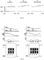
- the Ga/In concentration ratio increases towards the back contact, which is called “back grading” or “normal grading” (see Fig. 4 (b) )
- back grading or "normal grading”
- the Ga/In concentration ratio increases towards the buffer layer (“front grading")
- front grading the voltage of the device is enhanced, which again benefits the cell efficiency.
- CIGS is deposited from only one deposition source for each metal, e.g. from sources in the sequence Ga-Cu-In or In-Cu-Ga, either no front grading or no back grading is achieved.
- Fig. 5 (a) shows such a configuration.
- an additional metal deposition source is required, for examples a second Ga source enabling the sequence Ga-Cu-In-Ga (or Ga-In-Cu-Ga).
- Fig. 5 (b) Such a configuration is depicted in Fig. 5 (b) .
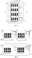
- every deposition-source block contains an array of deposition sources in a certain sequence, for example Ga-In-Cu followed by Cu-In-Ga, or Ga-In followed by Cu-In-Ga, or as depicted in Fig. 6 .
- Any combination of sources and blocks can be used in a deposition process.
- An array of deposition-source blocks may be placed within one deposition chamber 8, within consecutive deposition chambers, or within one or several deposition chambers having an internal separation feature 14 such as a shield or wall.
- a known measurement device When there are several deposition-source blocks, a known measurement device usually needs to be placed after every block. Since known measurement devices are heat-sensitive and since metal evaporation sources have to be operated at temperatures in the vicinity of 1000 °C or above, evaporation-source blocks cannot be placed close to each other because room is required for protection of the measurement devices from material deposition and heat radiation. Hence, deposition machines can become very large and complicated, and the film stack may cool down while moving through the measurement zone before reaching the following evaporation-source block.
- CIGS must be understood as a typical CIGS solar cell that is based on the semiconductor layer CIGS, which can be Cu(In,Ga)Se 2 or a related compound formed from any combination of the elements Cu, Ag, In, Ga, Al, Se, S, Te yielding a semiconductor in the form (Cu,Ag) x (In,Ga,Al) y (Se,S,Te) z , for example, the compound Cu(In,Ga) (Se,S) 2 .
- this class of compounds also comprises non-stoichiometric compounds such as Cu 0.9 (In,Ga) 1.1 Se 2 , or Cu(In,Ga) 3 Se 5 , etc., over wide ranges of compositions.
- Such compounds typically, but not always, contain a small amount of an alkali metal - added on purpose actively or passively - for example Na, K, or Li.
- the present invention is directed to a method as set forth in claim 1 for manufacturing a compound film comprising a substrate and at least one additional layer, the compound film satisfying predefined compound film properties, in particular being predefined values for compound-film thickness, compound-film overall composition and compositional profile, the latter being defined as a compound-film composition as a function of a position on or in the compound film.
- the method comprising the steps of:
- the method is characterized in that the substrate is a flexible foil, made at least in part of metal, polymer, or ceramic, and that said foil can be rolled up.
- the method is characterized in that the substrate is at least partially coated by one or several additional layers.
- the method is characterized in that the substrate is a plate of a material that is at least partially made of glass, metal, or polymer, and wherein the plates are continuously fed, one after the other, in order to be coated.
- the method is characterized in that the substrate is coated by one or several additional layers, wherein the same or different coatings can be applied on either side of the substrate.
- the method is characterized in that the step of measuring the compound film properties is performed by a measurement device that is moved in directions perpendicular and/or parallel to a traveling direction of the substrate, enabling measurements at different locations of the substrate, in particular across an entire width of the substrate.
- the method is characterized by further comprising the step of individually adjusting a deposition rate of the deposition sources.
- the method is characterized in that the deposition sources are arranged in a plurality of deposition-source blocks.
- the method is characterized in that at least a part of the measurement device is arranged opposite to the deposition sources with regard to the substrate. Therewith, the measurement device is protected from being coated and can be brought very close to the substrate or even touching the substrate without the risk of scratching the film.
- the method is characterized by positioning the measurement device in-between deposition-source blocks.
- the method is characterized in that the step of adjusting the deposition source is performed by modifying temperature, power supply or gas supply.
- the method is characterized in that the measurement device comprises an x-ray detector for detecting characteristic fluorescence radiation from appropriately excited atoms in the substrate and/or any of the additional layers, where said x-ray detector is capable if distinguishing the energies or wavelengths of the radiation and the respective radiation intensities.
- the method is characterized in that the measurement device comprises an excitation source, which excites atoms in fractions or all of the compound film and possibly also in a part or all of the substrate.
- the method is characterized in that the excitation source is an electron source, where the penetration depth of the electrons can be adjusted by changing the electron acceleration voltage.
- the method is characterized in that the excitation source is an x-ray source, where at least a part of the exciting x-rays are high enough in energy to induce K and L lines in the fluorescence spectrum of at least a part of the excited atom species.
- the method is characterized in that the excitation source comprises an x-ray source in combination with an electron source, where the x-ray source is capable of exciting atoms in all additional layers and in the substrate, while the electron source is capable of exciting only parts of the additional layers and/or the substrate.
- the method is characterized in that the compound film is a polycrystalline semiconductor compound of the form (Cu,Ag)(In,Ga,Al)(Se,S) 2 , particularly the compounds Cu(In,Ga)Se 2 or Cu(In,Ga) (Se, S) 2 .
- the method is characterized in that the substrate is a polyimide foil, which is particularly transparent for x-ray radiation, coated by an electrically conductive layer consisting of a single material.
- the method is characterized in that the electrically conductive layer on the foil is made of Mo.
- the method is characterized in that the electrically conductive layer on the foil is made of a metal nitride.
- the present invention improves deposition control for deposition of compound films comprising at least two chemical elements, such as CIGS.
- the invention increases the degree of freedom, to which elemental deposition profile shapes can be created, and enables to ensure consistent and reliable film properties.
- the deposition control improvement is achieved by employing one or several measurement sensors, together forming one measurement device, which allow determining film thickness, average film composition of the complete film (overall composition), as well as film composition in one or several fractions of the layer.
- the measurement device can be a fluorescence spectrometer, where the fluorescence radiation to be detected is x-ray radiation. Such a measurement is non-destructive and hence does not cause material quality loss in the probed portions of the films.
- the essential components of such a spectrometer typically are an excitation source (or alternatively at least two excitation sources) and a detector, all aligned in a way suitable for efficient measurement-signal detection and properly cooled and shielded.
- Source and detector do not necessarily have to be in the same housing, they can also be spatially separated, for example, they can be placed one on the back and one on the front side of the film to be probed.
- the excitation source typically emits x-rays or electrons.
- the detector detects the wavelengths of the fluorescence radiation and the intensities of the radiation of such wavelengths.
- the detector may be sensitive to the energies or frequencies of the fluorescence radiation, which in the end is equivalent to sensitivity to wavelengths due to the interrelation of radiation wavelength, energy, and frequency.
- the detector works usually either sequentially, e.g. by measuring one wavelength after the other, or simultaneously, e.g. by measuring all energies in the spectrum simultaneously with the help of a multi-channel analyzer.
- the wavelengths of the detected radiation are characteristic for the atom species present in the film.
- the intensity of radiation of a certain wavelength depends on the number of atoms of the corresponding atom species present in the probed part of the film.
- wavelength and intensity measurements allow quantifying the composition and, once the system has been calibrated, also the thickness of a film.
- all or only a part of the film to be measured can be probed.
- a negligible or significant part or the complete fluorescence signal of a certain wavelength is re-absorbed within the film (or in adjacent layers or in the substrate) and hence cannot reach the detector.
- excitation and fluorescence wavelengths different fractions of the film (or the entire film) to be measured are probed. Ideally, several combinations are used at the same time, such that several fractions of the film are probed at the same time.
- Such a fluorescence spectrometer is capable of determining film thickness, film overall composition, and film composition in one or several fractions of the layer, either in one or else in consecutive measurement steps.
- the signals of the measurement device 10 can be used by a control device such as a computer 11 to determine whether or not the output of a deposition source, or of a part of a deposition source 12, needs to be adjusted or not. Adjustment of source output can be achieved, for example, by modification of the source temperature, the power fed to the source, or the gas environment of the source. The closer to the deposition zone a measurement device can be positioned, i.e., the shorter the way a certain portion of a film needs to travel to come past the measurement device, the sooner the decision about the need for adjustment can be taken, which prevents more effectively the occurrence of faulty deposition and eventually of low production yield.
- a method is disclosed that improves deposition control such that the number of installed, controllable deposition sources requiring precise control can be increased without having to increase the number of measurement devices, and such that the flexibility for placement of such deposition sources and for source arrangements is enhanced.
- a fourth deposition source can be controlled ( Fig. 5b ).
- This enhanced flexibility allows to reliably deposit films (or layers) with well-defined and particularly beneficial compositional gradients (see Fig. 5 ).
- higher solar cell and module conversion efficiencies can be achieved and/or the thickness of the film can be reduced without or with reduced loss in conversion efficiency.
- This is realizable by using a measurement device capable of determining compound-film thickness, compound-film overall composition, and compositional profile, the latter being defined as a compound-film composition as a function of a position on or in the compound film.
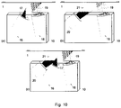
- a further embodiment of the present invention uses a measurement device 10 comprising, for example, an x-ray source 16 and an x-ray detector 18, placed in the same housing as the detector depicted in Fig. 10a , or in different housings, for example one part identified by 22 comprising the detector above the substrate 1 and one part identified by 23 comprising the source below the substrate 1, as schematically illustrated in Fig. 11a .
- the x-ray source 16 may emit monochromatic or broadband x-ray radiation 17.
- the radiation 17 of the x-ray source 16 is used to excite atoms in all layers and in the substrate 1.
- the excited atoms relax by emitting fluorescent radiation 19 of discrete wavelengths.
- a part of this fluorescent radiation 19 is in the x-ray regime and is therein classified according to the transitions in the radiating atoms as K, L, M, etc. lines.
- the K lines of the fluorescent radiation 19 are those with the smallest wavelengths and usually the highest penetration depths (the lowest absorption coefficients) in a material. Typically, the absorption of K lines within a layer of about 1 ⁇ m can be neglected; hence K lines can be taken to measure the total number of atoms of a certain element in the complete film.
- the L lines occur at higher wavelengths, where absorption within a layer is significant. The intensity of L-line radiation in a material falls exponentially due to the absorption.
- the L-line radiation can be completely absorbed within the film such that it cannot be detected anymore. Even if the penetration depth of L-line radiation is larger than the film thickness, there will still be significantly more L-line radiation from atoms closer to the surface, due to the exponential intensity decrease with thickness.
- the typical penetration depth of L-line radiation from a particular element in a material varies from element to element and from material to material.
- K-line fluorescence radiation detected outside the film by a detector will stem from atoms distributed throughout the film, while L-line fluorescence radiation will stem from atoms located closer to the surface. In this way, composition in different depths of one or several films can be measured. In particular, the measurement is sensitive to changes in the compositional profile, which is what is primarily needed for process control: Any change of the deposition process should be detectable and allow corrective action to be taken.
- a CIGS film with a Ga/In compositional double grading through the film can be characterized by using the In K lines for measurement of total In content in the film (corresponding to the average In concentration) and using the In L lines for measurement of the In content in the top part of the film.
- the same measurement could be done correspondingly with Ga lines instead of In lines, or with Ga lines in addition to the In lines.
- Another embodiment uses a measurement device 10 comprising an electron source 20 and an x-ray detector, placed in the same housing as the one in Fig. 10b , or in different housings, for example one part above the substrate 1 and one part below the substrate 1.
- the electrons 21 of the electron source 20 are used to excite atoms in certain parts of the film or films.
- the penetration depth and the excitation region and volume in a film are determined by the energy of the impinging electrons and by the material properties of the probed film.
- the energies of the electrons 21 from the electron source 20 for example by changing the electron acceleration voltage, atoms in different depths of a film are excited.
- fluorescence radiation 19 from the excited atoms can be detected and hence composition in different depths of one or several films can be measured.
- the measurement is sensitive to changes in the compositional profile.
- a rough depth profile of the In/Ga concentration ratio can be established. Any changes in that profile are detectable and allow adjusting the deposition-process parameters.
- Yet another embodiment uses a measurement device 10 comprising an x-ray source 16, an electron source 20, and an x-ray detector 18, placed in the same housing as in Fig. 10c or in different housings, for example one part above the substrate 1 and one part below the substrate 1.
- the x-ray source 16 and the x-ray detector 18 can be used to measure overall composition and thickness, for example by analyzing K-line fluorescence radiation.
- the exciting electrons can penetrate into different depths of a film, where they excite further atoms, hence giving rise to additional contributions to the fluorescence radiation, for example, the K-line fluorescence radiation.
- the x-ray source 16 and/or the electron source 20 is switched off periodically or from time to time, then separation of the signals is possible and overall composition and thickness as well as depth profiles can be extracted from the measurements.
- the measurement is sensitive to changes in the compositional profile.
- a control device such as a computer 11 receives signals from the measurement device 10 that are interpreted by the control device as a deviation of film thickness, film overall composition, and/or film compositional profile from pre-defined values, then the control device can take corrective action on the deposition process by feeding back a signal to the concerned deposition sources 12 ( Fig. 3 ).
- the feedback signal can initiate a change or changes in material deposition rate of one or several deposition sources, or of a part or parts of one or several deposition sources.
- a change in material deposition rate of a source or a part thereof can be achieved, for example, by modification of the supplied heating or sputter power or by modifying the local gas environment (pressure).
- a fast feedback signal is advantageous in order to take corrective action on the deposition process quickly, which allows preventing effectively the occurrence of faulty deposition and eventually of low production yield.
- a further embodiment of the present invention is disclosed which allows the control of film properties across the full width of wide substrates, perpendicular to the traveling direction of coated or uncoated substrates ( Fig. 7 ).
- Such control enables fine-tuning the material output rates of a wide deposition source over the full width of the source, not only in one or few points. This is particularly important if the relative deposition rates in different locations of a wide deposition source change with time, for example, because the source's reservoir of material to be deposited changes or because local heating/cooling or pressure characteristics change.
- the method furthermore allows controlling and fine-tuning deposition sources 12 consisting of at least two narrower deposition-source units 15 of similar or differing design and arranged side by side with or without gaps in between ( Fig. 8 ), for example, two or more narrower deposition-source units, or, as another example, an array of several point sources distributed along a line, where each point source corresponds to a deposition-source unit.
- a still further embodiment of the present invention is disclosed, which allows the control of the deposition sources arranged in two or more deposition-source blocks, each block consisting of the same or a different arrangement of one or several deposition sources, by using only one or only few measurement devices. This is achieved by moving each measurement device 10 not only across substrates (perpendicular to the traveling direction of the substrates), but also parallel to the traveling direction of the substrates to measure also in-between deposition source blocks 13, such as illustrated in Fig. 9b for the case of two deposition-source blocks.
- Another approach would be to use measurement devices 10 after every deposition-source block 13. But because good deposition sources do not change their deposition rate characteristics quickly, it is possible to sequentially employ only one measurement device in a large number of different locations. After completion of every measurement cycle, the measurement results can be compared to the results from previous measurement cycles and corrective actions on the deposition sources can be taken, if necessary. In this way, one or only few moving measurement devices suffice for controlling all deposition sources and hence can replace a larger number of non-moveable measurement devices.
- a further embodiment of the present invention is disclosed, which allows to employ a measurement device close to or even in the deposition zone, enabling a feedback signal for deposition source control with minimum delay, or even enabling real-time deposition source control by measurement of film properties in the deposition zone, while the film is still being grown.
- a particularly suitable way to achieve this is to place the measurement device 10 (or parts 22, 23 thereof) behind the substrate, such that the substrate is located in-between the measurement device (or parts 22, 23 thereof) and the deposition sources, for example as illustrated in Figs. 11a and 11b .
- the substrate protects the measurement device from material deposition and also to some extent from thermal radiation.
- the entire measurement device is placed behind the substrate, it cannot interfere with the atomic flux from the deposition sources, hence it is possible to move consecutive deposition-source blocks closer together while still measuring with the measurement device in-between ( Fig. 11c ), with no shadowing effects as they would occur with a measurement device placed on the front side of the substrate.
- placing a measurement device behind the substrate has the advantage that the measurement device can be positioned very close to or even touching the substrate. Because the measurement device is on the back side of the substrate, there is no risk of scratching sensitive, as deposited films. Having the measurement device placed close to the substrate means that the detection count rate of, for example, fluorescence radiation is high, since the count rate falls off rapidly with the square of the distance between film and detector. In turn, high count rates enable to use a short measurement time and hence to employ only one measurement device in many different locations.
- Still a further method is disclosed that allows correcting fluctuations in the measurement device results stemming from excitation source and/or detector drift with time, and/or from variations in source-film and/or film-detector distances.
- Distance variations can occur especially due to the moving substrates, especially if the substrates are flexible, and due to a certain amount of irreproducibility in measurement device placement in different locations.
- the measurement signal from underlying layers, or from the substrate needs to be analyzed as a reference signal. However, this signal often is received together with the main measurement signal and hence does not need any additional measurement sensors.
- the reference layer should happen to be inhomogeneous in thickness, it is required that, prior to the measurement of the compound film properties using the measurement device, the thickness profile of the reference layer is determined and used to correct the signal from the measurement device.
- the thickness profile of the reference layer can already be determined during deposition of the reference layer, for example by using a well-known quartz crystal microbalance or of optical emission spectrometry.
- the reference layer can be the back contact, typically Mo, or additional layers deposited prior to CIGS deposition or the substrate, or even a layer deposited on the back side of the substrate.
- the deposition processes of these further layers can be controlled using the same measurement device by feeding back the measurement information to the respective deposition sources. If the reference signal stems from a layer or substrate sufficiently thick, i.e. thicker than the penetration or exit length of the excitation or fluorescence radiation, then the thickness of this reference layer or substrate does not need to be known exactly, as long as it always is thick enough.
- the signal of the reference layer can be used to control the reference-layer-deposition process at the same time as the compound film deposition process.
- the back contact can be taken as reference layer and the back contact deposition process (often Mo deposition by dc sputtering) can be controlled at the same time as the CIGS deposition process.
- the time lag between deposition and measurement of the reference layer can become large, depending on the machine configuration. But if the reference layer does not need very tight control, such as Mo for solar cell applications, it can be acceptable if the reference layer characteristics deviate from the specifications for a limited period of time.
- the deposition processes for all these layers can be controlled simultaneously using the same measurement device by feeding back the measurement data to the respective deposition source controllers.
- Long-term drift of detector and/or source can be corrected in this case of negligible distance variations by occasionally measuring the composition and thickness of a suitable, stable, inert piece of material or coating located at an accessible place where it neither can move nor be coated with, for example, the coating materials, such as Se.
Landscapes
- Chemical & Material Sciences (AREA)
- Engineering & Computer Science (AREA)
- Chemical Kinetics & Catalysis (AREA)
- Materials Engineering (AREA)
- Mechanical Engineering (AREA)
- Metallurgy (AREA)
- Organic Chemistry (AREA)
- Physical Vapour Deposition (AREA)
- Analysing Materials By The Use Of Radiation (AREA)
- Manufacturing & Machinery (AREA)
- Chemical Vapour Deposition (AREA)
Claims (17)
- Procédé de fabrication d'une couche de film composite sur un substrat (1), la couche de film composite répondant à des propriétés prédéfinies, en particulier ayant des valeurs prédéfinies pour l'épaisseur, la composition globale et le profil de composition, ce dernier étant défini en tant que composition comme une fonction d'une position sur ou dans la couche de film composite, le procédé comprenant les étapes consistant à:- déposer au moins deux éléments chimiques (A, B) sur le substrat (1) en utilisant des sources de dépôt (12) qui sont agencées en une pluralité de blocs de sources de dépôt (13),- maintenir le dépôt des au moins deux éléments chimiques (A, B) tandis que le substrat (1) et les sources de dépôt (12) sont déplacés les uns par rapport aux autres,- positionner un dispositif de mesure (10) entre les blocs de sources de dépôt (13),- mesurer les propriétés de la couche de film composite par le dispositif de mesure (10), les propriétés de la couche de film composite étant au moins un élément parmi l'épaisseur, la composition globale et la composition à une ou plusieurs positions de la couche de film composite,- comparer les valeurs prédéfinies pour les propriétés de couche de film composite avec les propriétés de couche de film composite mesurées, et- ajuster le dépôt des au moins deux éléments chimiques (A, B) dans le cas où les propriétés de couche de film composite mesurées ne concordent pas avec les propriétés de couche de film composite prédéfinies,dans lequel au moins une partie du dispositif de mesure (10) est agencé à l'opposé des sources de dépôt (12) par rapport au substrat (1), et dans lequel le dispositif de mesure (10) comprend un détecteur de rayons X (18) et une source d'excitation sous la forme d'une source d'électrons (20) ou une source de rayons X (16).
- Procédé selon la revendication 1, caractérisé en ce que le substrat (1) est une feuille flexible composée au moins en partie de métal, de polymère ou de céramique, et en ce que ladite feuille peut être enroulée.
- Procédé selon la revendication 1 ou 2, caractérisé en ce que le substrat (1) est au moins partiellement recouvert d'une ou plusieurs couches supplémentaires (2, 3, 4, 5, 6, 7).
- Procédé selon la revendication 1, caractérisé en ce que le substrat (1) est une plaque de matériau qui est constituée au moins partiellement de verre, de métal ou de polymère, et dans lequel les plaques sont alimentées en continu, l'une après l'autre, pour pouvoir être recouvertes.
- Procédé selon l'une des revendications 1 à 4, caractérisé en ce que le substrat (1) est recouvert par une ou plusieurs couches supplémentaires (2, 3, 4, 5, 6, 7), dans lequel il est possible d'appliquer un même revêtement ou des revêtements différents sur l'un ou l'autre des côtés du substrat (1).
- Procédé selon l'une des revendications 3 à 5, caractérisé en ce que l'étape qui consiste à mesurer les propriétés de la couche de film composite est effectuée par un dispositif de mesure (10) qui est déplacé dans des directions perpendiculaires et/ou parallèles à un sens de déplacement du substrat (1), permettant ainsi des mesures à des endroits différents du substrat (1), en particulier sur toute la largeur du substrat (1).
- Procédé selon l'une des revendications 1 à 6, caractérisé en ce qu'il comprend en outre l'étape consistant à ajuster individuellement une vitesse de dépôt des sources de dépôt (12).
- Procédé selon l'une des revendications 1 à 7, caractérisé en ce que l'étape qui consiste à ajuster la source de dépôt (13) est effectuée en modifiant la température, l'alimentation électrique ou l'alimentation en gaz.
- Procédé selon l'une des revendications 1 à 8, caractérisé en ce que le détecteur de rayons X (18) est capable de détecter un rayonnement fluorescent caractéristique (19) provenant d'atomes correctement excités dans le substrat (1) et/ou toute couche supplémentaire (2, 3, 4, 5, 6, 7), et dans lequel ledit détecteur de rayons X (18) est capable de distinguer les énergies ou les longueurs d'onde du rayonnement (17) et les intensités de rayonnement respectives.
- Procédé selon l'une des revendications 1 à 9, caractérisé en ce que la source d'excitation excite les atomes en fractions ou bien toute la couche de film composite, et éventuellement aussi une partie ou la totalité du substrat (1).
- Procédé selon la revendication 10, caractérisé en ce que dans la source d'électrons (20) la profondeur de pénétration des électrons (21) peut être ajustée en modifiant la tension d'accélération des électrons.
- Procédé selon la revendication 10, caractérisé en ce que dans la source de rayons X (16) au moins une partie des rayons X excitants sont suffisamment énergétiques pour induire des lignes K et L dans le spectre de fluorescence d'au moins une partie des espèces d'atomes excités.
- Procédé selon la revendication 1 ou 10, caractérisé en ce que la source d'excitation comprend la source de rayons X (16) en combinaison avec la source d'électrons (20), la source de rayons X (16) étant capable d'exciter des atomes dans toutes les couches supplémentaires (2, 3, 4, 5, 6, 7) et dans le substrat (1), tandis que la source d'électrons (20) est capable d'exciter uniquement des parties des couches supplémentaires (2, 3, 4, 5, , 6 7) et/ou du substrat (1).
- Procédé selon l'une des revendications 1 à 13, caractérisé en ce que le film composite est un composé semi-conducteur polycristallin de la forme (Cu, Ag) (In, Ga, Al) (Se, S)2, en particulier les composés Cu (In, Ga) Se2 ou Cu (In, Ga) (Se, S)2.
- Procédé selon l'une des revendications 1 à 14, caractérisé en ce que le substrat (1) est une feuille polyimide, qui est en particulier transparente au rayonnement des rayons X, recouverte d'une couche électriquement conductrice composée d'un matériau unique.
- Procédé selon la revendication 15, caractérisé en ce que la couche électriquement conductrice sur la feuille est constituée de Mo.
- Procédé selon la revendication 15, caractérisé en ce que la couche électriquement conductrice sur la feuille est constituée d'un nitrure de métal.
Priority Applications (3)
| Application Number | Priority Date | Filing Date | Title |
|---|---|---|---|
| HUE17204498A HUE052503T2 (hu) | 2007-09-12 | 2007-09-12 | Berendezés kompozit film gyártására |
| EP17210307.9A EP3333280B1 (fr) | 2007-09-12 | 2007-09-12 | Procédé de fabrication d'un film d'un composé avec graduation compositionnelle |
| EP17204498.4A EP3327170B1 (fr) | 2007-09-12 | 2007-09-12 | Appareil pour fabriquer un film d'un composé |
Applications Claiming Priority (1)
| Application Number | Priority Date | Filing Date | Title |
|---|---|---|---|
| PCT/EP2007/059600 WO2009033503A1 (fr) | 2007-09-12 | 2007-09-12 | Procédé de fabrication d'un film composite |
Related Child Applications (4)
| Application Number | Title | Priority Date | Filing Date |
|---|---|---|---|
| EP17210307.9A Division EP3333280B1 (fr) | 2007-09-12 | 2007-09-12 | Procédé de fabrication d'un film d'un composé avec graduation compositionnelle |
| EP17210307.9A Division-Into EP3333280B1 (fr) | 2007-09-12 | 2007-09-12 | Procédé de fabrication d'un film d'un composé avec graduation compositionnelle |
| EP17204498.4A Division EP3327170B1 (fr) | 2007-09-12 | 2007-09-12 | Appareil pour fabriquer un film d'un composé |
| EP17204498.4A Division-Into EP3327170B1 (fr) | 2007-09-12 | 2007-09-12 | Appareil pour fabriquer un film d'un composé |
Publications (2)
| Publication Number | Publication Date |
|---|---|
| EP2188406A1 EP2188406A1 (fr) | 2010-05-26 |
| EP2188406B1 true EP2188406B1 (fr) | 2018-03-07 |
Family
ID=39431126
Family Applications (3)
| Application Number | Title | Priority Date | Filing Date |
|---|---|---|---|
| EP17204498.4A Active EP3327170B1 (fr) | 2007-09-12 | 2007-09-12 | Appareil pour fabriquer un film d'un composé |
| EP07803444.4A Active EP2188406B1 (fr) | 2007-09-12 | 2007-09-12 | Procédé de fabrication d'un film composite |
| EP17210307.9A Active EP3333280B1 (fr) | 2007-09-12 | 2007-09-12 | Procédé de fabrication d'un film d'un composé avec graduation compositionnelle |
Family Applications Before (1)
| Application Number | Title | Priority Date | Filing Date |
|---|---|---|---|
| EP17204498.4A Active EP3327170B1 (fr) | 2007-09-12 | 2007-09-12 | Appareil pour fabriquer un film d'un composé |
Family Applications After (1)
| Application Number | Title | Priority Date | Filing Date |
|---|---|---|---|
| EP17210307.9A Active EP3333280B1 (fr) | 2007-09-12 | 2007-09-12 | Procédé de fabrication d'un film d'un composé avec graduation compositionnelle |
Country Status (4)
| Country | Link |
|---|---|
| US (2) | US8927051B2 (fr) |
| EP (3) | EP3327170B1 (fr) |
| HU (1) | HUE052503T2 (fr) |
| WO (1) | WO2009033503A1 (fr) |
Families Citing this family (34)
| Publication number | Priority date | Publication date | Assignee | Title |
|---|---|---|---|---|
| US20170236710A1 (en) * | 2007-09-05 | 2017-08-17 | Ascent Solar Technologies, Inc. | Machine and process for continuous, sequential, deposition of semiconductor solar absorbers having variable semiconductor composition deposited in multiple sublayers |
| US8648253B1 (en) * | 2010-10-01 | 2014-02-11 | Ascent Solar Technologies, Inc. | Machine and process for continuous, sequential, deposition of semiconductor solar absorbers having variable semiconductor composition deposited in multiple sublayers |
| EP3327170B1 (fr) | 2007-09-12 | 2020-11-04 | Flisom AG | Appareil pour fabriquer un film d'un composé |
| US20130230933A1 (en) * | 2008-09-06 | 2013-09-05 | Soltrium Technology, Ltd. Shenzhen | Methods for fabricating thin film solar cells |
| KR101103770B1 (ko) * | 2009-10-12 | 2012-01-06 | 이화여자대학교 산학협력단 | 화합물 반도체 태양 전지 및 그 제조 방법 |
| WO2011082179A1 (fr) * | 2009-12-28 | 2011-07-07 | Global Solar Energy, Inc. | Appareil et procédés de mélange et de déposition de compositions photovoltaïques en film mince |
| US8865259B2 (en) * | 2010-04-26 | 2014-10-21 | Singulus Mocvd Gmbh I.Gr. | Method and system for inline chemical vapor deposition |
| KR20140037198A (ko) * | 2011-06-09 | 2014-03-26 | 싱귤러스 엠오씨브이디 게엠바하 아이. 지알. | 인라인 화학 기상 증착을 위한 방법 및 시스템 |
| IN2014KN02866A (fr) | 2012-06-20 | 2015-05-08 | Bengbu Design & Res Inst For Glass Industry | |
| US9366784B2 (en) | 2013-05-07 | 2016-06-14 | Corning Incorporated | Low-color scratch-resistant articles with a multilayer optical film |
| US9684097B2 (en) | 2013-05-07 | 2017-06-20 | Corning Incorporated | Scratch-resistant articles with retained optical properties |
| US9110230B2 (en) | 2013-05-07 | 2015-08-18 | Corning Incorporated | Scratch-resistant articles with retained optical properties |
| US9703011B2 (en) | 2013-05-07 | 2017-07-11 | Corning Incorporated | Scratch-resistant articles with a gradient layer |
| US9359261B2 (en) | 2013-05-07 | 2016-06-07 | Corning Incorporated | Low-color scratch-resistant articles with a multilayer optical film |
| KR101799087B1 (ko) * | 2013-06-27 | 2017-11-20 | 쌩-고벵 글래스 프랑스 | 나트륨-인듐 술피드 버퍼 층을 갖는 박층 태양 전지용 층 시스템 |
| US20150101534A1 (en) * | 2013-10-16 | 2015-04-16 | Chung-Shan Institute Of Science And Technology | Vapor Deposition Equipment for Fabricating CIGS Film |
| EP2887405A1 (fr) * | 2013-12-23 | 2015-06-24 | Saint-Gobain Glass France | Système à couches pour cellules solaires à couche mince |
| US9335444B2 (en) | 2014-05-12 | 2016-05-10 | Corning Incorporated | Durable and scratch-resistant anti-reflective articles |
| US11267973B2 (en) | 2014-05-12 | 2022-03-08 | Corning Incorporated | Durable anti-reflective articles |
| KR20170018937A (ko) * | 2014-06-16 | 2017-02-20 | 어플라이드 머티어리얼스, 인코포레이티드 | 정적 어레이 증착 프로세스들에 대한 폐루프 증착 제어를 통해 대면적 기판을 프로세싱하기 위한 장치 및 방법 |
| US9790593B2 (en) | 2014-08-01 | 2017-10-17 | Corning Incorporated | Scratch-resistant materials and articles including the same |
| JP2018536177A (ja) | 2015-09-14 | 2018-12-06 | コーニング インコーポレイテッド | 高光線透過性かつ耐擦傷性反射防止物品 |
| EP3559306B1 (fr) | 2016-12-22 | 2022-10-05 | Flisom AG | Source linéaire destinée au dépôt en phase vapeur dotée d'au moins trois éléments chauffants électriques |
| EP3559302A1 (fr) | 2016-12-22 | 2019-10-30 | Flisom AG | Source linéaire destinée au dépôt en phase vapeur équipée d'écrans thermiques |
| EP3559303A1 (fr) | 2016-12-22 | 2019-10-30 | Flisom AG | Source d'évaporation linéaire |
| EP3559304A1 (fr) | 2016-12-22 | 2019-10-30 | Flisom AG | Source de vapeur linéaire |
| EP3559305B1 (fr) | 2016-12-22 | 2025-07-16 | Flisom AG | Système rouleau à rouleau de dépôt en phase vapeur |
| AT15574U3 (de) * | 2017-05-11 | 2018-05-15 | Plansee Se | Flexibles Bauteil mit Schichtaufbau mit metallischer Lage |
| CN107731956B (zh) * | 2017-09-07 | 2022-07-05 | 东君新能源有限公司 | 一种薄膜太阳能电池吸收层制备工艺控制方法 |
| KR20230035447A (ko) * | 2017-09-20 | 2023-03-13 | 어플라이드 머티어리얼스, 인코포레이티드 | 기판 상의 세라믹 층의 두께를 제어하기 위한 방법 및 처리 시스템 |
| CN114085038A (zh) | 2018-08-17 | 2022-02-25 | 康宁股份有限公司 | 具有薄的耐久性减反射结构的无机氧化物制品 |
| US11973158B2 (en) | 2018-12-19 | 2024-04-30 | Idemitsu Kosan Co.,Ltd. | Photoelectric conversion element and method for manufacturing photoelectric conversion element |
| US12386101B2 (en) | 2020-07-09 | 2025-08-12 | Corning Incorporated | Textured region of a substrate to reduce specular reflectance incorporating surface features with an elliptical perimeter or segments thereof, and method of making the same |
| US11823964B2 (en) | 2021-04-16 | 2023-11-21 | Taiwan Semiconductor Manufacturing Co., Ltd. | Deposition system and method |
Family Cites Families (110)
| Publication number | Priority date | Publication date | Assignee | Title |
|---|---|---|---|---|
| US3552352A (en) * | 1968-02-13 | 1971-01-05 | Du Pont | Electron beam vaporization coating apparatus |
| US3843881A (en) * | 1973-01-11 | 1974-10-22 | Phillips Petroleum Co | Detection of elements by irradiating material and measuring scattered radiation at two energy levels |
| US3978510A (en) | 1974-07-29 | 1976-08-31 | Bell Telephone Laboratories, Incorporated | Heterojunction photovoltaic devices employing i-iii-vi compounds |
| US3995162A (en) | 1975-08-08 | 1976-11-30 | Gen Dynamics Corp | Apparatus and method for automated x-raying of quantities of small articles |
| US4162528A (en) | 1976-05-18 | 1979-07-24 | Bell Telephone Laboratories, Incorporated | X-ray-fluorescence measurement of thin film thicknesses |
| GB2070849B (en) | 1980-02-27 | 1983-11-09 | Gen Electric Co Ltd | Cathodoluminescent lamps |
| US4465575A (en) | 1981-09-21 | 1984-08-14 | Atlantic Richfield Company | Method for forming photovoltaic cells employing multinary semiconductor films |
| US4523051A (en) | 1983-09-27 | 1985-06-11 | The Boeing Company | Thin films of mixed metal compounds |
| AU570309B2 (en) | 1984-03-26 | 1988-03-10 | Unisearch Limited | Buried contact solar cell |
| US4611091A (en) | 1984-12-06 | 1986-09-09 | Atlantic Richfield Company | CuInSe2 thin film solar cell with thin CdS and transparent window layer |
| US4612411A (en) | 1985-06-04 | 1986-09-16 | Atlantic Richfield Company | Thin film solar cell with ZnO window layer |
| US4684761A (en) | 1986-04-09 | 1987-08-04 | The Boeing Company | Method for making graded I-III-VI2 semiconductors and solar cell obtained thereby |
| US4705698A (en) | 1986-10-27 | 1987-11-10 | Chronar Corporation | Isolation of semiconductor contacts |
| US4892592A (en) | 1987-03-26 | 1990-01-09 | Solarex Corporation | Thin film semiconductor solar cell array and method of making |
| US5141564A (en) | 1988-05-03 | 1992-08-25 | The Boeing Company | Mixed ternary heterojunction solar cell |
| US5439575A (en) | 1988-06-30 | 1995-08-08 | Board Of Trustees Of The University Of Illinois | Hybrid method for depositing semi-conductive materials |
| US5014288A (en) | 1989-04-20 | 1991-05-07 | Measurex Corporation | X-ray coating weight controller and sensor |
| JPH0394444A (ja) * | 1989-05-10 | 1991-04-19 | Fujitsu Ltd | 膜厚測定方法と装置および薄膜製造装置 |
| US5078804A (en) | 1989-06-27 | 1992-01-07 | The Boeing Company | I-III-VI2 based solar cell utilizing the structure CuInGaSe2 CdZnS/ZnO |
| US5078803A (en) | 1989-09-22 | 1992-01-07 | Siemens Solar Industries L.P. | Solar cells incorporating transparent electrodes comprising hazy zinc oxide |
| FI87492C (fi) | 1990-06-12 | 1993-01-11 | Valmet Paper Machinery Inc | Foerfarande och anordning foer maetning och reglering av bestrykningsmaengden |
| JP2974513B2 (ja) | 1992-09-03 | 1999-11-10 | キヤノン株式会社 | 屋根材一体型太陽電池モジュール |
| JP3337255B2 (ja) | 1993-02-15 | 2002-10-21 | 松下電器産業株式会社 | カルコパイライト構造半導体薄膜とその製造方法、薄膜太陽電池の製造方法、および発光装置の製造方法 |
| US5441897A (en) | 1993-04-12 | 1995-08-15 | Midwest Research Institute | Method of fabricating high-efficiency Cu(In,Ga)(SeS)2 thin films for solar cells |
| US5356839A (en) | 1993-04-12 | 1994-10-18 | Midwest Research Institute | Enhanced quality thin film Cu(In,Ga)Se2 for semiconductor device applications by vapor-phase recrystallization |
| US5627871A (en) * | 1993-06-10 | 1997-05-06 | Nanodynamics, Inc. | X-ray tube and microelectronics alignment process |
| US5803976A (en) | 1993-11-09 | 1998-09-08 | Imperial Chemical Industries Plc | Vacuum web coating |
| US5633033A (en) | 1994-04-18 | 1997-05-27 | Matsushita Electric Industrial Co., Ltd. | Method for manufacturing chalcopyrite film |
| WO1995033081A1 (fr) * | 1994-05-31 | 1995-12-07 | Toray Industries, Inc. | Substrat filme et procede et dispositif de production de ce substrat |
| US5483568A (en) | 1994-11-03 | 1996-01-09 | Kabushiki Kaisha Toshiba | Pad condition and polishing rate monitor using fluorescence |
| DE4442824C1 (de) | 1994-12-01 | 1996-01-25 | Siemens Ag | Solarzelle mit Chalkopyrit-Absorberschicht |
| US5532102A (en) | 1995-03-30 | 1996-07-02 | Xerox Corporation | Apparatus and process for preparation of migration imaging members |
| JP3527815B2 (ja) | 1996-11-08 | 2004-05-17 | 昭和シェル石油株式会社 | 薄膜太陽電池の透明導電膜の製造方法 |
| JP3397637B2 (ja) | 1997-06-11 | 2003-04-21 | キヤノン株式会社 | 太陽電池一体型屋根板、その製造方法、及びその施工方法 |
| US5930586A (en) | 1997-07-03 | 1999-07-27 | Motorola, Inc. | Method and apparatus for in-line measuring backside wafer-level contamination of a semiconductor wafer |
| US6258620B1 (en) | 1997-10-15 | 2001-07-10 | University Of South Florida | Method of manufacturing CIGS photovoltaic devices |
| JPH11126916A (ja) | 1997-10-24 | 1999-05-11 | Sharp Corp | 集積形薄膜太陽電池及びその製造方法 |
| US6428848B1 (en) | 1998-08-06 | 2002-08-06 | Toray Industries, Inc. | Method for producing a metal evaporated article |
| US6121624A (en) | 1998-08-24 | 2000-09-19 | Lucent Technologies, Inc. | Method for controlled implantation of elements into the surface or near surface of a substrate |
| AU731869B2 (en) | 1998-11-12 | 2001-04-05 | Kaneka Corporation | Solar cell module |
| US6202591B1 (en) | 1998-11-12 | 2001-03-20 | Flex Products, Inc. | Linear aperture deposition apparatus and coating process |
| US7666490B1 (en) | 1999-02-10 | 2010-02-23 | Toyo Boseki Kabushiki Kaisha | Functional roll film and vacuum evaporation apparatus capable of producing the functional roll film |
| AU4398700A (en) | 1999-04-07 | 2000-10-23 | Siemens Solar Gmbh | Device and method for removing thin layers on a support material |
| US6714936B1 (en) | 1999-05-25 | 2004-03-30 | Nevin, Iii Rocky Harry W. | Method and apparatus for displaying data stored in linked nodes |
| EP1076222A1 (fr) * | 1999-08-10 | 2001-02-14 | Corus Aluminium Walzprodukte GmbH | Mesure de l'épaisseur de tôles en aluminium par fluorescence aux rayons X |
| DE60045678D1 (de) | 1999-09-28 | 2011-04-14 | Kaneka Corp | Methode zur Steuerung des Herstellungsverfahrens einer photoelektrischen Umwandlungsvorrichtung |
| US6830626B1 (en) | 1999-10-22 | 2004-12-14 | Kurt J. Lesker Company | Method and apparatus for coating a substrate in a vacuum |
| US6300593B1 (en) | 1999-12-07 | 2001-10-09 | First Solar, Llc | Apparatus and method for laser scribing a coated substrate |
| DE10013635A1 (de) * | 2000-03-18 | 2001-09-20 | Gerhard Regittnig | CIS-Dünnfilm-Photovoltaik |
| US7194197B1 (en) | 2000-03-16 | 2007-03-20 | Global Solar Energy, Inc. | Nozzle-based, vapor-phase, plume delivery structure for use in production of thin-film deposition layer |
| US6372538B1 (en) | 2000-03-16 | 2002-04-16 | University Of Delaware | Fabrication of thin-film, flexible photovoltaic module |
| US6310281B1 (en) | 2000-03-16 | 2001-10-30 | Global Solar Energy, Inc. | Thin-film, flexible photovoltaic module |
| DE10019045B4 (de) | 2000-04-18 | 2005-06-23 | Carl Zeiss Smt Ag | Verfahren zum Herstellen von Viellagensystemen |
| WO2002005352A2 (fr) | 2000-07-06 | 2002-01-17 | Bp Corporation North America Inc. | Modules photovoltaiques partiellement transparents |
| FR2816822B1 (fr) | 2000-11-23 | 2003-05-09 | Ge Med Sys Global Tech Co Llc | Procede et dispositif de galactographie en radiologie mammographique par soustraction |
| US6611576B1 (en) | 2001-02-12 | 2003-08-26 | Advanced Micro Devices, Inc. | Automated control of metal thickness during film deposition |
| US6402905B1 (en) | 2001-03-16 | 2002-06-11 | 4 Wave, Inc | System and method for controlling deposition thickness using a mask with a shadow that varies along a radius of a substrate |
| US6629879B1 (en) | 2001-05-08 | 2003-10-07 | Advanced Micro Devices, Inc. | Method of controlling barrier metal polishing processes based upon X-ray fluorescence measurements |
| US6562405B2 (en) | 2001-09-14 | 2003-05-13 | University Of Delaware | Multiple-nozzle thermal evaporation source |
| US6559372B2 (en) | 2001-09-20 | 2003-05-06 | Heliovolt Corporation | Photovoltaic devices and compositions for use therein |
| US6660538B2 (en) | 2001-10-29 | 2003-12-09 | Energy Photovoltaics | Non-contacting deposition control of chalcopyrite thin films |
| CA2489231A1 (fr) | 2002-06-13 | 2003-12-24 | Ims Health Incorporated | Methode et systeme servant a aider a prendre une mesure correctrice relativement a une activite de marche pharmaceutique |
| WO2004017352A2 (fr) | 2002-07-30 | 2004-02-26 | Siemens Aktiengesellschaft | Procede de metallisation sous vide d'un support avec un materiau a fluorescence x sous forme d'aiguille et materiau a fluorescence x correspondant |
| SE523930C3 (sv) | 2002-09-03 | 2004-08-18 | Sixsteps Ab Ideon Science Park | Datorprogramprodukt med tillhörande metoder för att söka i en databas med objekt, koppla samman objekt i en sådan databas och exportera data från minst en godtycklig databas |
| AU2003275239A1 (en) * | 2002-09-30 | 2004-04-23 | Miasole | Manufacturing apparatus and method for large-scale production of thin-film solar cells |
| DE10256909B3 (de) | 2002-11-30 | 2004-07-29 | Hahn-Meitner-Institut Berlin Gmbh | Verfahren zur Herstellung einer Chalkogenid-Halbleiterschicht mit optischer in-situ-Prozesskontrolle und Vorrichtung zur Verfahrensdurchführung |
| DE10259258B4 (de) | 2002-12-11 | 2006-03-16 | Würth Solar Gmbh & Co. Kg | Verfahren zur Herstellung einer Verbindungshalbleiterschicht mit Alkalimetallzusatz |
| WO2004090995A1 (fr) * | 2003-04-09 | 2004-10-21 | Matsushita Electric Industrial Co., Ltd. | Cellule solaire |
| US7512297B2 (en) | 2003-05-02 | 2009-03-31 | John Farah | Polymide substrate bonded to other substrate |
| US7170001B2 (en) | 2003-06-26 | 2007-01-30 | Advent Solar, Inc. | Fabrication of back-contacted silicon solar cells using thermomigration to create conductive vias |
| US7649141B2 (en) | 2003-06-30 | 2010-01-19 | Advent Solar, Inc. | Emitter wrap-through back contact solar cells on thin silicon wafers |
| KR100716704B1 (ko) * | 2004-03-03 | 2007-05-14 | 산요덴키가부시키가이샤 | 퇴적 두께 측정 방법, 재료층의 형성 방법, 퇴적 두께 측정장치 및 재료층의 형성 장치 |
| SE0400582D0 (sv) | 2004-03-05 | 2004-03-05 | Forskarpatent I Uppsala Ab | Method for in-line process control of the CIGS process |
| US7736940B2 (en) * | 2004-03-15 | 2010-06-15 | Solopower, Inc. | Technique and apparatus for depositing layers of semiconductors for solar cell and module fabrication |
| US7276724B2 (en) | 2005-01-20 | 2007-10-02 | Nanosolar, Inc. | Series interconnected optoelectronic device module assembly |
| WO2006047207A2 (fr) | 2004-10-21 | 2006-05-04 | University Of Delaware | Formation de films de seleniure, de sulfure ou de melange seleniure-sulfure sur metal ou sur des substrats de metal |
| WO2006053128A2 (fr) | 2004-11-10 | 2006-05-18 | Daystar Technologies, Inc. | Systeme utilisant une plaque pour la formation de cellules solaires a film mince |
| US7576017B2 (en) | 2004-11-10 | 2009-08-18 | Daystar Technologies, Inc. | Method and apparatus for forming a thin-film solar cell using a continuous process |
| US20070186971A1 (en) | 2005-01-20 | 2007-08-16 | Nanosolar, Inc. | High-efficiency solar cell with insulated vias |
| JP4474324B2 (ja) | 2005-04-28 | 2010-06-02 | パナソニック株式会社 | 成膜装置 |
| US20070102035A1 (en) | 2005-10-31 | 2007-05-10 | Xiai (Charles) Yang | Method and Structure for Integrated Solar Cell LCD Panel |
| US8107777B2 (en) | 2005-11-02 | 2012-01-31 | John Farah | Polyimide substrate bonded to other substrate |
| US7442413B2 (en) | 2005-11-18 | 2008-10-28 | Daystar Technologies, Inc. | Methods and apparatus for treating a work piece with a vaporous element |
| TWI331213B (en) | 2005-11-29 | 2010-10-01 | Horiba Ltd | Sample analyzing method, sample analyzing apparatus,and recording medium |
| JP5662001B2 (ja) | 2005-12-21 | 2015-01-28 | クロメック リミテッド | 半導体デバイス及びその製造方法 |
| US8845866B2 (en) | 2005-12-22 | 2014-09-30 | General Electric Company | Optoelectronic devices having electrode films and methods and system for manufacturing the same |
| WO2007092568A2 (fr) | 2006-02-07 | 2007-08-16 | 3Jam, Inc. | Procédés et dispositifs utilisés pour intégrer une pluralité d'utilisateurs dans une conversation sur un réseau de communication |
| SI1989740T2 (sl) | 2006-02-28 | 2019-10-30 | Q Cells Se | Postopek označevanja sončnih celic in sončna celica |
| US7235736B1 (en) * | 2006-03-18 | 2007-06-26 | Solyndra, Inc. | Monolithic integration of cylindrical solar cells |
| US7736913B2 (en) * | 2006-04-04 | 2010-06-15 | Solopower, Inc. | Composition control for photovoltaic thin film manufacturing |
| US20070277875A1 (en) * | 2006-05-31 | 2007-12-06 | Kishor Purushottam Gadkaree | Thin film photovoltaic structure |
| US7964418B2 (en) | 2006-08-18 | 2011-06-21 | Solyndra Llc | Real time process monitoring and control for semiconductor junctions |
| US20080083448A1 (en) | 2006-09-29 | 2008-04-10 | Borden Peter G | Interconnect for thin film photovoltaic modules |
| US7777640B2 (en) | 2007-07-31 | 2010-08-17 | Tryggvi Emilsson | Use of heating and/or ventilation ductwork to broadcast alarm conditions |
| US8225496B2 (en) | 2007-08-31 | 2012-07-24 | Applied Materials, Inc. | Automated integrated solar cell production line composed of a plurality of automated modules and tools including an autoclave for curing solar devices that have been laminated |
| EP3327170B1 (fr) | 2007-09-12 | 2020-11-04 | Flisom AG | Appareil pour fabriquer un film d'un composé |
| US8771419B2 (en) | 2007-10-05 | 2014-07-08 | Solopower Systems, Inc. | Roll to roll evaporation tool for solar absorber precursor formation |
| US8163090B2 (en) | 2007-12-10 | 2012-04-24 | Solopower, Inc. | Methods structures and apparatus to provide group VIA and IA materials for solar cell absorber formation |
| KR101368904B1 (ko) | 2007-12-31 | 2014-02-28 | 주성엔지니어링(주) | 박막형 태양전지 및 그 제조방법 |
| US8415559B2 (en) | 2008-02-08 | 2013-04-09 | Solopower, Inc. | Method for forming copper indium gallium chalcogenide layer with shaped gallium profile |
| US20090291231A1 (en) | 2008-05-21 | 2009-11-26 | Applied Materials, Inc. | Method and apparatus for producing a solar cell module with integrated laser patterning |
| JP5048843B2 (ja) | 2008-09-22 | 2012-10-17 | 株式会社アルバック | 太陽電池の製造方法 |
| JP5185171B2 (ja) | 2009-03-24 | 2013-04-17 | 本田技研工業株式会社 | 薄膜太陽電池の光吸収層の形成方法 |
| US7829783B2 (en) | 2009-05-12 | 2010-11-09 | Miasole | Isolated metallic flexible back sheet for solar module encapsulation |
| TW201112438A (en) | 2009-09-25 | 2011-04-01 | Zhi-Huang Lai | Target, manufacturing process of manufacturing thin film solar cell and the products thereof |
| US8012788B1 (en) | 2009-10-21 | 2011-09-06 | Sunlight Photonics Inc. | Multi-stage formation of thin-films for photovoltaic devices |
| FR2954265B1 (fr) | 2009-12-22 | 2012-05-04 | Jcdecaux Sa | Systeme automatique de stockage de cycles, cycle pour un tel systeme et structure d'accueil pour un tel cycle. |
| WO2011106902A2 (fr) | 2010-03-05 | 2011-09-09 | Flisom Ag | Procédé et appareil de fabrication de modules photovoltaïques intégrés de façon monolithique et module photovoltaïque |
| EP2577732B1 (fr) | 2010-05-28 | 2019-03-13 | Flisom AG | Procédé et dispositif de fabrication de modules à couche mince avec interconnexions par points et trous de liaison |
| US8048706B1 (en) | 2010-10-14 | 2011-11-01 | Miasole | Ablative scribing of solar cell structures |
-
2007
- 2007-09-12 EP EP17204498.4A patent/EP3327170B1/fr active Active
- 2007-09-12 HU HUE17204498A patent/HUE052503T2/hu unknown
- 2007-09-12 US US12/677,665 patent/US8927051B2/en active Active
- 2007-09-12 WO PCT/EP2007/059600 patent/WO2009033503A1/fr not_active Ceased
- 2007-09-12 EP EP07803444.4A patent/EP2188406B1/fr active Active
- 2007-09-12 EP EP17210307.9A patent/EP3333280B1/fr active Active
-
2013
- 2013-07-26 US US13/952,420 patent/US9666745B2/en active Active
Also Published As
| Publication number | Publication date |
|---|---|
| EP3327170A1 (fr) | 2018-05-30 |
| EP2188406A1 (fr) | 2010-05-26 |
| HUE052503T2 (hu) | 2021-05-28 |
| EP3333280A1 (fr) | 2018-06-13 |
| US9666745B2 (en) | 2017-05-30 |
| EP3327170B1 (fr) | 2020-11-04 |
| EP3333280B1 (fr) | 2026-04-01 |
| US20100247745A1 (en) | 2010-09-30 |
| US8927051B2 (en) | 2015-01-06 |
| WO2009033503A1 (fr) | 2009-03-19 |
| US20130312664A1 (en) | 2013-11-28 |
Similar Documents
| Publication | Publication Date | Title |
|---|---|---|
| EP3327170B1 (fr) | Appareil pour fabriquer un film d'un composé | |
| Ma et al. | Origin of band-tail and deep-donor states in Cu2ZnSnS4 solar cells and their suppression through Sn-poor composition | |
| Probst et al. | Rapid CIS-process for high efficiency PV-modules: development towards large area processing | |
| US7576017B2 (en) | Method and apparatus for forming a thin-film solar cell using a continuous process | |
| EP2660857B1 (fr) | Dispositif photovoltaïque à couche mince | |
| US8859405B2 (en) | Method of fabricating high efficiency CIGS solar cells | |
| AU2005219926B2 (en) | Method and apparatus for in-line process control of the CIGS process | |
| KR20140071327A (ko) | 태양 전지 셀의 제조 방법 및 태양 전지 모듈 | |
| Fuster et al. | System for manufacturing complete Cu (In, Ga) Se2 solar cells in situ under vacuum | |
| US20150179839A1 (en) | Contact layers for photovoltaic devices | |
| WO2003038871A1 (fr) | Commande de depot sans contact de couches minces de chalcopyrite | |
| JP7070946B2 (ja) | 薄膜太陽電池用層構造を製造するための方法 | |
| JP2014216479A (ja) | 光電変換素子の製造方法 | |
| Salomé | Chalcogenide thin films for solar cells: growth and properties | |
| do Carmo Alves | Cu (In, Ga) Se2 Thin Film Solar Cell by Magnetron Sputtering | |
| Schulte | Investigations of the reactive co-sputtering deposition of Cu (In 1-x, Ga x)(S 1-y, Se y) 2 absorber layers for thin film solar cells | |
| Al-Saab | Chalcogenides for solar applications |
Legal Events
| Date | Code | Title | Description |
|---|---|---|---|
| PUAI | Public reference made under article 153(3) epc to a published international application that has entered the european phase |
Free format text: ORIGINAL CODE: 0009012 |
|
| 17P | Request for examination filed |
Effective date: 20100309 |
|
| AK | Designated contracting states |
Kind code of ref document: A1 Designated state(s): AT BE BG CH CY CZ DE DK EE ES FI FR GB GR HU IE IS IT LI LT LU LV MC MT NL PL PT RO SE SI SK TR |
|
| AX | Request for extension of the european patent |
Extension state: AL BA HR MK RS |
|
| DAX | Request for extension of the european patent (deleted) | ||
| STAA | Information on the status of an ep patent application or granted ep patent |
Free format text: STATUS: EXAMINATION IS IN PROGRESS |
|
| 17Q | First examination report despatched |
Effective date: 20170111 |
|
| GRAP | Despatch of communication of intention to grant a patent |
Free format text: ORIGINAL CODE: EPIDOSNIGR1 |
|
| STAA | Information on the status of an ep patent application or granted ep patent |
Free format text: STATUS: GRANT OF PATENT IS INTENDED |
|
| INTG | Intention to grant announced |
Effective date: 20170915 |
|
| GRAS | Grant fee paid |
Free format text: ORIGINAL CODE: EPIDOSNIGR3 |
|
| GRAJ | Information related to disapproval of communication of intention to grant by the applicant or resumption of examination proceedings by the epo deleted |
Free format text: ORIGINAL CODE: EPIDOSDIGR1 |
|
| GRAL | Information related to payment of fee for publishing/printing deleted |
Free format text: ORIGINAL CODE: EPIDOSDIGR3 |
|
| STAA | Information on the status of an ep patent application or granted ep patent |
Free format text: STATUS: EXAMINATION IS IN PROGRESS |
|
| GRAR | Information related to intention to grant a patent recorded |
Free format text: ORIGINAL CODE: EPIDOSNIGR71 |
|
| STAA | Information on the status of an ep patent application or granted ep patent |
Free format text: STATUS: GRANT OF PATENT IS INTENDED |
|
| GRAA | (expected) grant |
Free format text: ORIGINAL CODE: 0009210 |
|
| STAA | Information on the status of an ep patent application or granted ep patent |
Free format text: STATUS: THE PATENT HAS BEEN GRANTED |
|
| INTC | Intention to grant announced (deleted) | ||
| INTG | Intention to grant announced |
Effective date: 20180125 |
|
| AK | Designated contracting states |
Kind code of ref document: B1 Designated state(s): AT BE BG CH CY CZ DE DK EE ES FI FR GB GR HU IE IS IT LI LT LU LV MC MT NL PL PT RO SE SI SK TR |
|
| REG | Reference to a national code |
Ref country code: GB Ref legal event code: FG4D |
|
| REG | Reference to a national code |
Ref country code: CH Ref legal event code: EP Ref country code: AT Ref legal event code: REF Ref document number: 976649 Country of ref document: AT Kind code of ref document: T Effective date: 20180315 |
|
| REG | Reference to a national code |
Ref country code: IE Ref legal event code: FG4D |
|
| REG | Reference to a national code |
Ref country code: DE Ref legal event code: R096 Ref document number: 602007054168 Country of ref document: DE |
|
| REG | Reference to a national code |
Ref country code: NL Ref legal event code: MP Effective date: 20180307 |
|
| REG | Reference to a national code |
Ref country code: LT Ref legal event code: MG4D |
|
| PG25 | Lapsed in a contracting state [announced via postgrant information from national office to epo] |
Ref country code: ES Free format text: LAPSE BECAUSE OF FAILURE TO SUBMIT A TRANSLATION OF THE DESCRIPTION OR TO PAY THE FEE WITHIN THE PRESCRIBED TIME-LIMIT Effective date: 20180307 Ref country code: LT Free format text: LAPSE BECAUSE OF FAILURE TO SUBMIT A TRANSLATION OF THE DESCRIPTION OR TO PAY THE FEE WITHIN THE PRESCRIBED TIME-LIMIT Effective date: 20180307 Ref country code: CY Free format text: LAPSE BECAUSE OF FAILURE TO SUBMIT A TRANSLATION OF THE DESCRIPTION OR TO PAY THE FEE WITHIN THE PRESCRIBED TIME-LIMIT Effective date: 20180307 Ref country code: FI Free format text: LAPSE BECAUSE OF FAILURE TO SUBMIT A TRANSLATION OF THE DESCRIPTION OR TO PAY THE FEE WITHIN THE PRESCRIBED TIME-LIMIT Effective date: 20180307 |
|
| REG | Reference to a national code |
Ref country code: AT Ref legal event code: MK05 Ref document number: 976649 Country of ref document: AT Kind code of ref document: T Effective date: 20180307 |
|
| PG25 | Lapsed in a contracting state [announced via postgrant information from national office to epo] |
Ref country code: BG Free format text: LAPSE BECAUSE OF FAILURE TO SUBMIT A TRANSLATION OF THE DESCRIPTION OR TO PAY THE FEE WITHIN THE PRESCRIBED TIME-LIMIT Effective date: 20180607 Ref country code: GR Free format text: LAPSE BECAUSE OF FAILURE TO SUBMIT A TRANSLATION OF THE DESCRIPTION OR TO PAY THE FEE WITHIN THE PRESCRIBED TIME-LIMIT Effective date: 20180608 Ref country code: LV Free format text: LAPSE BECAUSE OF FAILURE TO SUBMIT A TRANSLATION OF THE DESCRIPTION OR TO PAY THE FEE WITHIN THE PRESCRIBED TIME-LIMIT Effective date: 20180307 Ref country code: SE Free format text: LAPSE BECAUSE OF FAILURE TO SUBMIT A TRANSLATION OF THE DESCRIPTION OR TO PAY THE FEE WITHIN THE PRESCRIBED TIME-LIMIT Effective date: 20180307 |
|
| REG | Reference to a national code |
Ref country code: FR Ref legal event code: PLFP Year of fee payment: 12 |
|
| PG25 | Lapsed in a contracting state [announced via postgrant information from national office to epo] |
Ref country code: PL Free format text: LAPSE BECAUSE OF FAILURE TO SUBMIT A TRANSLATION OF THE DESCRIPTION OR TO PAY THE FEE WITHIN THE PRESCRIBED TIME-LIMIT Effective date: 20180307 Ref country code: IT Free format text: LAPSE BECAUSE OF FAILURE TO SUBMIT A TRANSLATION OF THE DESCRIPTION OR TO PAY THE FEE WITHIN THE PRESCRIBED TIME-LIMIT Effective date: 20180307 Ref country code: RO Free format text: LAPSE BECAUSE OF FAILURE TO SUBMIT A TRANSLATION OF THE DESCRIPTION OR TO PAY THE FEE WITHIN THE PRESCRIBED TIME-LIMIT Effective date: 20180307 Ref country code: NL Free format text: LAPSE BECAUSE OF FAILURE TO SUBMIT A TRANSLATION OF THE DESCRIPTION OR TO PAY THE FEE WITHIN THE PRESCRIBED TIME-LIMIT Effective date: 20180307 Ref country code: EE Free format text: LAPSE BECAUSE OF FAILURE TO SUBMIT A TRANSLATION OF THE DESCRIPTION OR TO PAY THE FEE WITHIN THE PRESCRIBED TIME-LIMIT Effective date: 20180307 |
|
| PG25 | Lapsed in a contracting state [announced via postgrant information from national office to epo] |
Ref country code: CZ Free format text: LAPSE BECAUSE OF FAILURE TO SUBMIT A TRANSLATION OF THE DESCRIPTION OR TO PAY THE FEE WITHIN THE PRESCRIBED TIME-LIMIT Effective date: 20180307 Ref country code: AT Free format text: LAPSE BECAUSE OF FAILURE TO SUBMIT A TRANSLATION OF THE DESCRIPTION OR TO PAY THE FEE WITHIN THE PRESCRIBED TIME-LIMIT Effective date: 20180307 Ref country code: SK Free format text: LAPSE BECAUSE OF FAILURE TO SUBMIT A TRANSLATION OF THE DESCRIPTION OR TO PAY THE FEE WITHIN THE PRESCRIBED TIME-LIMIT Effective date: 20180307 |
|
| REG | Reference to a national code |
Ref country code: DE Ref legal event code: R097 Ref document number: 602007054168 Country of ref document: DE |
|
| PG25 | Lapsed in a contracting state [announced via postgrant information from national office to epo] |
Ref country code: PT Free format text: LAPSE BECAUSE OF FAILURE TO SUBMIT A TRANSLATION OF THE DESCRIPTION OR TO PAY THE FEE WITHIN THE PRESCRIBED TIME-LIMIT Effective date: 20180709 |
|
| PLBE | No opposition filed within time limit |
Free format text: ORIGINAL CODE: 0009261 |
|
| STAA | Information on the status of an ep patent application or granted ep patent |
Free format text: STATUS: NO OPPOSITION FILED WITHIN TIME LIMIT |
|
| PG25 | Lapsed in a contracting state [announced via postgrant information from national office to epo] |
Ref country code: DK Free format text: LAPSE BECAUSE OF FAILURE TO SUBMIT A TRANSLATION OF THE DESCRIPTION OR TO PAY THE FEE WITHIN THE PRESCRIBED TIME-LIMIT Effective date: 20180307 |
|
| 26N | No opposition filed |
Effective date: 20181210 |
|
| PG25 | Lapsed in a contracting state [announced via postgrant information from national office to epo] |
Ref country code: SI Free format text: LAPSE BECAUSE OF FAILURE TO SUBMIT A TRANSLATION OF THE DESCRIPTION OR TO PAY THE FEE WITHIN THE PRESCRIBED TIME-LIMIT Effective date: 20180307 |
|
| PG25 | Lapsed in a contracting state [announced via postgrant information from national office to epo] |
Ref country code: MC Free format text: LAPSE BECAUSE OF FAILURE TO SUBMIT A TRANSLATION OF THE DESCRIPTION OR TO PAY THE FEE WITHIN THE PRESCRIBED TIME-LIMIT Effective date: 20180307 |
|
| PG25 | Lapsed in a contracting state [announced via postgrant information from national office to epo] |
Ref country code: LU Free format text: LAPSE BECAUSE OF NON-PAYMENT OF DUE FEES Effective date: 20180912 |
|
| REG | Reference to a national code |
Ref country code: CH Ref legal event code: PVP |
|
| PG25 | Lapsed in a contracting state [announced via postgrant information from national office to epo] |
Ref country code: MT Free format text: LAPSE BECAUSE OF NON-PAYMENT OF DUE FEES Effective date: 20180912 |
|
| PG25 | Lapsed in a contracting state [announced via postgrant information from national office to epo] |
Ref country code: TR Free format text: LAPSE BECAUSE OF FAILURE TO SUBMIT A TRANSLATION OF THE DESCRIPTION OR TO PAY THE FEE WITHIN THE PRESCRIBED TIME-LIMIT Effective date: 20180307 |
|
| PG25 | Lapsed in a contracting state [announced via postgrant information from national office to epo] |
Ref country code: HU Free format text: LAPSE BECAUSE OF FAILURE TO SUBMIT A TRANSLATION OF THE DESCRIPTION OR TO PAY THE FEE WITHIN THE PRESCRIBED TIME-LIMIT; INVALID AB INITIO Effective date: 20070912 |
|
| PG25 | Lapsed in a contracting state [announced via postgrant information from national office to epo] |
Ref country code: IS Free format text: LAPSE BECAUSE OF FAILURE TO SUBMIT A TRANSLATION OF THE DESCRIPTION OR TO PAY THE FEE WITHIN THE PRESCRIBED TIME-LIMIT Effective date: 20180707 |
|
| PGFP | Annual fee paid to national office [announced via postgrant information from national office to epo] |
Ref country code: IE Payment date: 20220920 Year of fee payment: 16 Ref country code: GB Payment date: 20220920 Year of fee payment: 16 Ref country code: DE Payment date: 20220920 Year of fee payment: 16 |
|
| PGFP | Annual fee paid to national office [announced via postgrant information from national office to epo] |
Ref country code: FR Payment date: 20220922 Year of fee payment: 16 Ref country code: BE Payment date: 20220920 Year of fee payment: 16 |
|
| PGFP | Annual fee paid to national office [announced via postgrant information from national office to epo] |
Ref country code: CH Payment date: 20220928 Year of fee payment: 16 |
|
| REG | Reference to a national code |
Ref country code: DE Ref legal event code: R119 Ref document number: 602007054168 Country of ref document: DE |
|
| REG | Reference to a national code |
Ref country code: CH Ref legal event code: PL |
|
| REG | Reference to a national code |
Ref country code: BE Ref legal event code: MM Effective date: 20230930 |
|
| GBPC | Gb: european patent ceased through non-payment of renewal fee |
Effective date: 20230912 |
|
| REG | Reference to a national code |
Ref country code: IE Ref legal event code: MM4A |
|
| PG25 | Lapsed in a contracting state [announced via postgrant information from national office to epo] |
Ref country code: IE Free format text: LAPSE BECAUSE OF NON-PAYMENT OF DUE FEES Effective date: 20230912 |
|
| PG25 | Lapsed in a contracting state [announced via postgrant information from national office to epo] |
Ref country code: GB Free format text: LAPSE BECAUSE OF NON-PAYMENT OF DUE FEES Effective date: 20230912 |
|
| PG25 | Lapsed in a contracting state [announced via postgrant information from national office to epo] |
Ref country code: CH Free format text: LAPSE BECAUSE OF NON-PAYMENT OF DUE FEES Effective date: 20230930 |
|
| PG25 | Lapsed in a contracting state [announced via postgrant information from national office to epo] |
Ref country code: IE Free format text: LAPSE BECAUSE OF NON-PAYMENT OF DUE FEES Effective date: 20230912 Ref country code: GB Free format text: LAPSE BECAUSE OF NON-PAYMENT OF DUE FEES Effective date: 20230912 Ref country code: FR Free format text: LAPSE BECAUSE OF NON-PAYMENT OF DUE FEES Effective date: 20230930 Ref country code: DE Free format text: LAPSE BECAUSE OF NON-PAYMENT OF DUE FEES Effective date: 20240403 Ref country code: CH Free format text: LAPSE BECAUSE OF NON-PAYMENT OF DUE FEES Effective date: 20230930 |
|
| PG25 | Lapsed in a contracting state [announced via postgrant information from national office to epo] |
Ref country code: BE Free format text: LAPSE BECAUSE OF NON-PAYMENT OF DUE FEES Effective date: 20230930 |
|
| REG | Reference to a national code |
Ref country code: CH Ref legal event code: R14 Free format text: ST27 STATUS EVENT CODE: U-0-0-R10-R14 (AS PROVIDED BY THE NATIONAL OFFICE) Effective date: 20260220 |