EP2188921B1 - Oscillateur optique à commande électrique pour une boucle à verrouillage de phase optique de sous-porteuse unique - Google Patents
Oscillateur optique à commande électrique pour une boucle à verrouillage de phase optique de sous-porteuse unique Download PDFInfo
- Publication number
- EP2188921B1 EP2188921B1 EP08789013A EP08789013A EP2188921B1 EP 2188921 B1 EP2188921 B1 EP 2188921B1 EP 08789013 A EP08789013 A EP 08789013A EP 08789013 A EP08789013 A EP 08789013A EP 2188921 B1 EP2188921 B1 EP 2188921B1
- Authority
- EP
- European Patent Office
- Prior art keywords
- optical
- electrical
- signal
- phase
- oscillator
- Prior art date
- Legal status (The legal status is an assumption and is not a legal conclusion. Google has not performed a legal analysis and makes no representation as to the accuracy of the status listed.)
- Not-in-force
Links
- 230000003287 optical effect Effects 0.000 title claims abstract description 290
- 230000010287 polarization Effects 0.000 claims description 15
- 230000010363 phase shift Effects 0.000 claims description 7
- 238000001914 filtration Methods 0.000 claims description 5
- 230000003321 amplification Effects 0.000 claims 2
- 238000003199 nucleic acid amplification method Methods 0.000 claims 2
- 238000011144 upstream manufacturing Methods 0.000 claims 1
- 230000003595 spectral effect Effects 0.000 description 24
- 201000002044 ossification of the posterior longitudinal ligament of spine Diseases 0.000 description 16
- 208000001040 ossification of the posterior longitudinal ligament of the spine Diseases 0.000 description 16
- 238000001228 spectrum Methods 0.000 description 12
- 239000004065 semiconductor Substances 0.000 description 11
- 230000005540 biological transmission Effects 0.000 description 9
- 239000000243 solution Substances 0.000 description 6
- 230000005672 electromagnetic field Effects 0.000 description 5
- 238000012546 transfer Methods 0.000 description 5
- 230000008901 benefit Effects 0.000 description 4
- 238000004891 communication Methods 0.000 description 4
- 238000010586 diagram Methods 0.000 description 4
- 230000009022 nonlinear effect Effects 0.000 description 4
- 230000008033 biological extinction Effects 0.000 description 3
- 230000001427 coherent effect Effects 0.000 description 3
- 238000010276 construction Methods 0.000 description 3
- 238000013461 design Methods 0.000 description 3
- 238000001514 detection method Methods 0.000 description 3
- 238000000034 method Methods 0.000 description 3
- 238000013519 translation Methods 0.000 description 3
- 230000015572 biosynthetic process Effects 0.000 description 2
- 238000005516 engineering process Methods 0.000 description 2
- 230000014509 gene expression Effects 0.000 description 2
- 238000012986 modification Methods 0.000 description 2
- 230000004048 modification Effects 0.000 description 2
- 230000010355 oscillation Effects 0.000 description 2
- 230000009467 reduction Effects 0.000 description 2
- 238000003786 synthesis reaction Methods 0.000 description 2
- 230000002238 attenuated effect Effects 0.000 description 1
- 230000015556 catabolic process Effects 0.000 description 1
- 230000008878 coupling Effects 0.000 description 1
- 238000010168 coupling process Methods 0.000 description 1
- 238000005859 coupling reaction Methods 0.000 description 1
- 238000006731 degradation reaction Methods 0.000 description 1
- 239000000835 fiber Substances 0.000 description 1
- 238000002347 injection Methods 0.000 description 1
- 239000007924 injection Substances 0.000 description 1
- 230000000737 periodic effect Effects 0.000 description 1
- 229920000729 poly(L-lysine) polymer Polymers 0.000 description 1
- 230000010349 pulsation Effects 0.000 description 1
- 230000035945 sensitivity Effects 0.000 description 1
Images

Classifications
-
- H—ELECTRICITY
- H04—ELECTRIC COMMUNICATION TECHNIQUE
- H04B—TRANSMISSION
- H04B10/00—Transmission systems employing electromagnetic waves other than radio-waves, e.g. infrared, visible or ultraviolet light, or employing corpuscular radiation, e.g. quantum communication
- H04B10/60—Receivers
- H04B10/61—Coherent receivers
- H04B10/63—Homodyne, i.e. coherent receivers where the local oscillator is locked in frequency and phase to the carrier signal
-
- H—ELECTRICITY
- H04—ELECTRIC COMMUNICATION TECHNIQUE
- H04B—TRANSMISSION
- H04B10/00—Transmission systems employing electromagnetic waves other than radio-waves, e.g. infrared, visible or ultraviolet light, or employing corpuscular radiation, e.g. quantum communication
- H04B10/60—Receivers
- H04B10/61—Coherent receivers
-
- H—ELECTRICITY
- H04—ELECTRIC COMMUNICATION TECHNIQUE
- H04B—TRANSMISSION
- H04B10/00—Transmission systems employing electromagnetic waves other than radio-waves, e.g. infrared, visible or ultraviolet light, or employing corpuscular radiation, e.g. quantum communication
- H04B10/60—Receivers
- H04B10/61—Coherent receivers
- H04B10/615—Arrangements affecting the optical part of the receiver
- H04B10/6151—Arrangements affecting the optical part of the receiver comprising a polarization controller at the receiver's input stage
Definitions
- the present invention relates to an electrically controlled optical oscillator for a single-side-subcarrier optical phase-locked loop.
- Optical phase-locked loops are optical devices used in frequency synthesis and in coherent demodulation in optical communication systems for local generation of an optical signal with a frequency and a phase that track those of an optical input signal.
- an OPLL is basically formed by an optical phase detector, an electrical loop filter, and an optical voltage-controlled oscillator (OVCO) comprising a non-modulated optical source, an electrical voltage-controlled oscillator, and an optical amplitude modulator, which is designed to modulate the optical carrier supplied by the non-modulated optical source with the electrical modulating signal supplied by the electrical voltage-controlled oscillator.
- OVCO optical voltage-controlled oscillator
- the phase detector receives an optical signal to be locked and a locked optical signal - i.e., one having a frequency and a phase "locked" to those of the optical input signal -, which is supplied by the OVCO, and supplies an electrical error signal indicating the difference of phase existing between the optical input signals.
- the electrical error signal generated by the phase detector is supplied to the loop filter, which has a transfer function of a low-pass type and supplies a filtered electrical error signal that is then supplied to the OVCO, which supplies the aforementioned locked optical signal, the instantaneous frequency of which varies proportionally with the amplitude of the filtered electrical signal.
- OVCOs are generally obtained with solid-state laser or tunable-semiconductor laser that can be modulated directly, which, although used in the past, present, however, certain drawbacks that markedly condition the use of the OPLLs in which they are inserted.
- OPLLs that use OVCOs based upon solid-state lasers are, however, difficult to apply to optical communications systems, in so far as it is somewhat difficult to find solid-state lasers functioning in the frequency grid set down by ITU (International Telecommunication Union).
- solid-state lasers are very voluminous and cumbersome, require a lot of power for their operation and are more costly than OPLLs that use OVCOs based upon semiconductor lasers.
- OPLLs that use OVCOs based upon semiconductor lasers require, however, the use of a distributed-feedback (DFB) technology, which requires the use of wide-band electronic feedback circuits on account of the considerable linewidth of directly controlled semiconductor lasers, and an injection current that is extremely high on account of the non-ideal operation of said devices.
- DFB distributed-feedback
- a PSK binary transmission system with coherent homodyne detection has a sensitivity that is better by 3.5 dB than a standard IM-DD transmission system with NRZ format.
- Said advantage may be used to reduce by approximately 3.5 dB the mean optical power required for each transmission channel. In terms of peak power there is hence obtained a reduction of approximately 6.5 dB, with consequent drastic reduction in the non-linear effects in the fibre, which are a source of degradation of the performance.
- a 4-PSK transmission system has a spectral occupation that is half that of a standard binary transmission system with NRZ format.
- OPLLs according to the known art are far from suitable for use in optical telecommunications systems based upon the most recent techniques of dense wavelength-division multiplexing (DWDM).
- DWDM dense wavelength-division multiplexing
- the aim of the present invention is to provide an electrically controlled optical oscillator that will enable the above drawback to be overcome at least in part.
- a single-side-subcarrier electrically controlled optical oscillator for an optical phase-locked loop and an optical phase-locked loop comprising said single-side-subcarrier electrically controlled optical oscillator are provided, as defined in the annexed claims.
- the present invention stems from the realization by the present applicant whereby the limitation indicated above of OPLLs based upon subcarrier modulation is due to the fact that the locked optical signal has a frequency spectrum comprising, in addition to a useful subcarrier for locking the optical signal received, also a spurious subcarrier of a power comparable to that of the useful subcarrier, as illustrated in Figure 1 , where f 0 is the frequency of an optical signal to be modulated and f VCO is the modulation frequency.
- this spurious subcarrier gives rise to beats with the DWDM optical signals, which considerably limit the performance of the OPLL.
- the operating range of frequencies of the VCO would have to be increased up to values such as to render necessary the use of particularly complex and hence costly VCOs.
- the idea underlying the present invention is to improve the performance of OPLLs with subcarrier modulation using an OVCO that will supply a locked optical signal having a frequency spectrum comprising a single optical subcarrier.
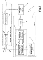
- Figure 2 illustrates the block diagram of an OPLL implementing the idea underlying the present invention.
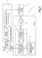
- the OPLL designated as a whole by 1, comprises an optical phase detector 2, an electrical loop filter 3, a single-side-subcarrier OVCO 4, and a polarization controller 5.
- the optical phase detector 2 comprises an optical coupler 6, which receives at input an optical signal to be locked S 1 and a locked optical signal S 2 supplied by the OVCO 4 and supplies at output a coupled optical signal S 3 .
- optical coupler 6 can be represented by an ideal 90° hybrid coupler, which is an optical device having two optical outputs, which supply, respectively, an optical signal S 3 and an optical signal S 4 the general expressions of which are the following:
- the phase detector 2 further comprises a photodetector 7, which receives the coupled optical signal S 3 generated by the optical coupler 6 and supplies an electrical error voltage signal V PD indicating the phase difference between the optical signal to be locked S 1 and the locked optical signal S 2 .
- the electrical error signal is then supplied to the electrical loop filter 3, which is a filter of the type commonly used in electrical phase-locked loops and supplies at output a filtered electrical error signal V PDF .
- the filtered electrical error signal V PDF is then supplied to the OVCO 4, which generates at output the aforementioned locked optical signal S 2 , the frequency of which varies proportionally with the amplitude of the filtered electrical error signal V PDP .
- the polarization controller 5 is set in a position corresponding to the input of the optical coupler 6 on which the optical signal to be locked is received, and modifies, in a way in itself known and hence not described in detail, the optical polarization of the optical signal to be locked in such a way that the optical polarizations of the optical signal to be locked and of the locked optical signal will be parallel to one another at input to the photodetector 7.
- the OVCO 4 comprises an electrical voltage-controlled oscillator (EVCO) 8, a continuous-wave laser source 9, an optical modulator 10, and an electrical directional coupler 11.
- EVCO electrical voltage-controlled oscillator
- optical modulator optical modulator
- electrical directional coupler 11.
- the EVCO 8 is an oscillator having a free frequency of oscillation of its own which can be defined in the design stage and the output of which is constituted by a sinusoidal signal the frequency deviation of which with respect to the free frequency of oscillation is proportional to the amplitude of the electrical signal supplied on its input.
- the EVCO 8 receives at input the filtered electrical error signal V PDF supplied by the electrical loop filter 3 and supplies at output an electrical modulating signal V EVCO constituted by a voltage having a sinusoidal pattern with a frequency that is a function of the amplitude of the filtered electrical error signal V PDF .
- the continuous-wave laser source 9 is constituted by a semiconductor-laser source with external cavity of the type commonly available on the market and produced using the DFB technology typical for applications of the DWDM type and generating an optical carrier S OC , i.e., a practically monochromatic optical signal, that is, a signal having an optical electromagnetic field with a "quasi ideally" sinusoidal pattern, and adjustable optical frequency.
- an optical carrier S OC i.e., a practically monochromatic optical signal, that is, a signal having an optical electromagnetic field with a "quasi ideally" sinusoidal pattern, and adjustable optical frequency.
- the electrical directional coupler 11 receives at input the (sinusoidal) signal V EVCO generated by the EVCO 8 and supplies on the electrical outputs two electrical (sinusoidal) modulating signals V EIN1 and V EIN2 at the same frequency and the phases of which respect a specific relationship, substantially a relationship of quadrature.
- V EVCO generated by the EVCO 8
- V EIN1 and V EIN2 electrical (sinusoidal) modulating signals
- the optical modulator 10 has two electrical inputs on which it receives the two electrical modulating signals V EIN1 and V EIN2 supplied by the electrical directional coupler 11, an optical input, on which it receives the optical signal to be modulated, and an optical output, on which it supplies the modulated signal.
- the optical modulator 10 is of the type designed to generate a single-side-subcarrier optical signal.
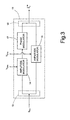
- the optical modulator 10 is conveniently of the type with both phase and amplitude modulation, an embodiment of which is illustrated in Figure 3 .
- the optical phase-and-amplitude modulator 10 comprises two optical couplers 13 and 16, two optical amplitude modulators 14, 15 and an adjustable optical phase-shifter 17, which can be implemented with an optical phase modulator controlled by an appropriate signal.
- the optical couplers 13 and 16 are arranged so as to form a first optical path and a second optical path.
- the first optical path comprises the optical amplitude modulator 14, applied on the input of which is the electrical signal V EIN1
- the second optical path comprises the optical amplitude modulator 15, applied on the input of which is the electrical signal V EIN2 .
- the optical phase-and-amplitude modulator 10 receives on the optical input the optical carrier S OC generated by the laser source 9 and supplies on the optical output the aforementioned locked optical signal S 2 , having phase and amplitude that depend upon the electrical signal V EVCO generated by the EVCO 8, as will be described hereinafter. Consequently, it is in general possible to consider the pair constituted by the electrical directional coupler 11 (alternatively, the electrical hybrid coupler) and by the optical phase-and-amplitude modulator 10 as optical modulator means 12, provided with an optical input, which receives the optical carrier S OC , an electrical input, which receives the electrical modulating signal, and an optical output, which supplies the optical modulated signal S 2 .
- the OVCO 4 functions in the so-called mode with suppressed carrier and with generation of a single subcarrier (single side subcarrier optical voltage-controlled oscillator, SS-SC-OVCO).
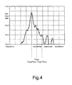
- the power spectrum of the output signal of the optical phase-and-amplitude modulator 10 contains:
- Both of the spurious lines are attenuated with respect to the main spectral line by a factor determined substantially by the extinction ratio of the modulator as regards the spurious line at the frequency F LASER , and by a factor determined jointly by the characteristics of the optical phase-and-amplitude modulator 10, and by the electrical directional coupler 11 as regards the spurious spectral line at the frequency F LASER + F EVCO .
- an optical signal is obtained having a single main spectral line (single subcarrier) with a frequency and phase proportional to the electrical driving signal of the EVCO 8, whence the name cited previously of "single-side-subcarrier optical voltage-controlled oscillator".
- the present invention enables, with the use of components commonly available on the market, provision of an OVCO 4 that is able to replace the traditional OVCOs obtained with tunable solid-state or semiconductor laser, or else OVCOs based upon subcarrier modulation (SC-OVCO).
- the optical signal S 2 supplied by the OVCO 4 has an optical spectrum that is constituted by a main spectral line (single subcarrier), the frequency and phase of which are controlled directly by the filtered electrical error signal V PDF at input to the OVCO 4, said input coinciding with that of the EVCO 8.
- OPLL 1 which in what follows will be referred to also as single-side-subcarrier optical phase-locked loop (SS-SC-OPLL), is similar to that of an OPLL that uses a traditional OVCO, obtained with solid-state laser or semiconductor laser, or else an OVCO based upon subcarrier modulation (SC-OPLL).
- SC-OPLL single-side-subcarrier optical phase-locked loop
- the difference between the phase of the optical signal S 1 and the phase of the main line of the optical signal S 2 supplied by the phase detector 2 represents an error signal used for driving the EVCO 8, which supplies at output a sinusoidal voltage V EVCO the frequency of which is proportional to said error.
- the main line is the one at the frequency F LASER + F EVCO (and the frequency line F LASER - F EVCO is hence the spurious one) of the output power spectrum of the optical phase-and-amplitude modulator 10.
- the choice of the spectral line of the output power spectrum of the optical phase-and-amplitude modulator 10 that must be used as main line can be obtained by adjusting the optical frequency F LASER of the optical carrier S OC supplied by the external-cavity semiconductor laser 9 in such a way that the frequency of the main line is as close as possible to the frequency F INPUT of the optical signal S 1 , i.e., it falls within the locking bandwidth of the OPLL 1.
- the frequency F INPUT of the optical signal S 1 is close to the frequency F LASER - F EVCO of the main spectral line of the output power spectrum of the optical phase-and-amplitude modulator 10
- the beat, introduced by the photodetection, between the frequency of the optical signal S 1 , i.e., F INPUT , and the three main frequencies of the spectrum of the optical signal S 2 i.e., F LASER , F LASER - F EVCO and F LASER + F EVCO , generates a series of spectral lines at different frequencies.
- One of the aforesaid spectral lines is in baseband (at exactly 0 Hz if the OPLL 1 is locked), whilst the other spectral lines are spurious and at frequencies of ⁇ n ⁇ F EVCO . Said spurious spectral lines are eliminated by the filtering introduced by the electrical loop filter 3, appropriately designed, and by the photodetector 7.
- an external optical modulator and an EVCO enables an extreme accuracy in the synthesis of the optical frequency, to the extent that this is limited only by the characteristics of the EVCO.
- EVCOs are commercially available with electrical frequencies that are even very high (50-60 GHz) and a relatively wide range of tunability (- 10-100 MHz).
- solid-state laser or semiconductor EVCO require instead an extreme accuracy in the control of the biasing current of directly modulated semiconductor lasers, which are somewhat problematical to produce.
- the scheme of construction of the OVCO proposed enables a practically ideal frequency translation, the linearity of which as a function of the applied voltage is limited only by the linearity of the EVCO and not by the optical components used.
- a further advantage is due to the translation in frequency not affected by any spurious amplitude modulation, thanks to the signal at output from the EVCO, the amplitude of which is constant throughout its range of operation.
- the translation in frequency is always accompanied by a spurious amplitude modulation that must necessarily be compensated for by a purposely provided electrical or optical circuit.
- the scheme of construction proposed in the present application enables generation of a spectrally purer locked signal S 2 .
- said locked signal S 2 comprises a single main spectral line, whilst in the case of SC-OPLL the main lines are two, and only one is used for locking, whilst the second is a spurious line having a power equal to the one used for locking, with consequent limitation of the fields of use of the SC-OPLL.
- the laser used as direct oscillator is a non-modulated (i.e., CW) laser. It is therefore possible to use an external-cavity semiconductor laser slowly tunable in wavelength. With this solution there is the advantage of having both a fast tunability on a limited range of frequencies thanks to the OVCO and a slow tunability on a wide range of wavelengths, thanks to the direct control of the parameters, available on every commercial tunable laser. In the other solutions, instead, non-commercial laser sources are required that are to be purposely developed.
- the operating condition whereby the points of operation at rest of the optical amplitude modulators inside the phase-and-amplitude modulator must coincide with the minima of the electro-optical transfer functions F(V) of the modulators themselves is not strictly necessary for proper operation of the OVCO 4.
- the power spectrum of the output signal of the optical phase-and-amplitude modulator 10 would contain a spectral line at the frequency F LASER having a non-negligible amplitude with respect to the main spectral line of interest (single subcarrier); said spectral line would be, however, in any case eliminated in the filtering performed by the electrical loop filter 3 and possibly also by the photodetector 7.
- the polarization controller 5 through which the optical polarizations of the optical signal to be locked and of the locked optical signal are kept parallel to one another at input to the photodetector 7 must not necessarily be set at the input of the optical coupler 6 on which the optical signal to be locked arrives, but can be set in any other point of the OPLL 1 in which, in any case, it is able to operate for keeping the optical polarizations of the optical signal to be locked and of the locked optical signal parallel to one another at input to the photodetector 7; for example, it could be set at the output of the optical phase-and-amplitude modulator 10.
- the EVCO 8 could be of a type different from the one previously described, and in particular, instead of being an electrical voltage-controlled oscillator, may also be an electrical current-controlled oscillator. In the latter case, therefore, the OVCO 4 would likewise become an optical current-controlled oscillator.
Landscapes
- Physics & Mathematics (AREA)
- Electromagnetism (AREA)
- Engineering & Computer Science (AREA)
- Computer Networks & Wireless Communication (AREA)
- Signal Processing (AREA)
- Optical Communication System (AREA)
- Semiconductor Lasers (AREA)
- Lasers (AREA)
- Optical Modulation, Optical Deflection, Nonlinear Optics, Optical Demodulation, Optical Logic Elements (AREA)
Claims (17)
- Oscillateur optique à commande électrique (4) pour une boucle à verrouillage de phase optique de sous-porteuse unique, comprenant :- des moyens formant oscillateur électrique à commande électrique (8) ayant une entrée configurée pour recevoir un signal d'entrée de commande électrique (VPDF) et une sortie configurée pour fournir un signal de sortie de commande électrique (VEVCO) ayant une fréquence (FEVCO) qui est fonction dudit signal d'entrée de commande électrique (VPDF) ;- une source laser à ondes entretenues (9) configurée pour fournir une porteuse optique (SOC) ; et- des moyens formant modulateur optique (12) ayant une entrée optique connectée à ladite source laser (9) pour recevoir ladite porteuse optique (SOC), une entrée électrique connectée à ladite sortie desdits moyens formant oscillateur électrique à commande électrique (8) pour recevoir ledit signal de sortie de commande électrique (VEVCO), et une sortie optique configurée pour moduler ladite porteuse optique (SOC) avec ledit signal de sortie de commande électrique (VEVCO) et générer ainsi un signal modulé optique (
S 2) ;
ledit oscillateur optique à commande électrique étant caractérisé en ce que lesdits moyens formant modulateur optique (12) sont du type configuré pour générer un signal modulé optique (S 2) avec une sous-porteuse optique unique. - Oscillateur optique à commande électrique (4) selon la revendication 1, dans lequel lesdits moyens formant modulateur optique (12) comprennent un modulateur de phase et d'amplitude optique.
- Oscillateur optique à commande électrique (4) selon la revendication 2, dans lequel lesdits moyens formant modulateur optique (12) comprennent en outre un dispositif électrique (11) ayant une entrée électrique configurée pour recevoir un signal d'entrée électrique, et deux sorties électriques, qui sont configurées pour fournir des signaux de sortie électriques respectifs ayant des fréquences égales à la fréquence du signal d'entrée électrique et des phases qui respectent une relation donnée ; ledit modulateur de phase et d'amplitude optique (10) ayant une entrée optique recevant ladite porteuse optique (SOC), une sortie optique fournissant ledit signal modulé optique (
S 2), et deux entrées électriques configurées pour recevoir lesdits signaux de sortie électriques fournis par ledit dispositif électrique (11). - Oscillateur optique à commande électrique (4) selon la revendication 3, dans lequel ledit modulateur de phase et d'amplitude optique (10) comprend un premier trajet optique et un second trajet optique en parallèle l'un l'autre, le premier trajet optique comprenant un premier modulateur d'amplitude optique (14) et un déphaseur optique ajustable (17) connecté en série audit premier modulateur d'amplitude optique (14) et configuré pour introduire un déphasage donné, le second trajet optique comprenant un second modulateur d'amplitude optique (15), lesdits premier et second modulateurs d'amplitude optique (14, 15) ayant des points respectifs de fonctionnement au repos et étant commandés respectivement par lesdits signaux de sortie électriques fournis par ledit dispositif électrique (11), et un déphaseur optique ajustable (17).
- Oscillateur optique à commande électrique (4) selon la revendication 4, dans lequel ladite relation est une relation de quadrature, et en outre, ledit déphasage donné est de 90°.
- Oscillateur optique à commande électrique (4) selon la revendication 5, dans lequel ledit dispositif électrique (11) est un coupleur directionnel.
- Oscillateur optique à commande électrique (4) selon la revendication 5, dans lequel ledit dispositif électrique (11) est un coupleur hybride 90°.
- Oscillateur optique à commande électrique (4) selon la revendication 5, dans lequel ledit dispositif électrique (11) est un répartiteur de puissance.
- Oscillateur optique à commande électrique (4) selon l'une quelconque des revendications précédentes, dans lequel ladite source laser (9) est un laser à cavité externe.
- Boucle à verrouillage de phase optique (1), comprenant :- des moyens formant détecteur de phase optique (2) ayant une première entrée optique configurée pour recevoir un signal optique devant être verrouillé (
S 1), une seconde entrée optique configurée pour recevoir un signal optique verrouillé (S 2), et une sortie électrique, configurée pour fournir un signal d'erreur électrique (VPD) indiquant la différence entre la phase dudit signal optique devant être verrouillé (S 1) et la phase dudit signal optique verrouillé (S 2) ; et- des moyens formant oscillateur optique à commande électrique (4) pour générer une sous-porteuse unique, ayant une entrée électrique configurée pour recevoir un signal de commande électrique (VPDF) qui est fonction dudit signal d'erreur électrique (VPD) et une sortie optique configurée pour fournir ledit signal optique verrouillé (S 2) ;
ladite boucle à verrouillage de phase optique étant caractérisée en ce que lesdits moyens formant oscillateur optique à commande électrique (4) sont prévus selon l'une quelconque des revendications précédentes. - Boucle à verrouillage de phase optique (1) selon la revendication 10, dans laquelle lesdits moyens formant détecteur de phase optique (2) comprennent :- des moyens formant coupleur optique (6) ayant une première entrée optique configurée pour recevoir ledit signal optique devant être verrouillé (
S 1), une seconde entrée optique configurée pour recevoir ledit signal optique verrouillé (S 2) et une sortie optique configurée pour fournir un signal optique couplé (S 3) ; et- des moyens formant photodétecteur (7) configurés pour recevoir ledit signal optique couplé (S 3) et pour fournir ledit signal d'erreur électrique (VPD). - Boucle à verrouillage de phase optique (1) selon la revendication 11, dans laquelle lesdits moyens formant coupleur optique (6) comprennent un coupleur optique 3dB.
- Boucle à verrouillage de phase optique (1) selon la revendication 12, dans laquelle lesdits moyens formant coupleur optique (6) comprennent un coupleur optique hybride 90°.
- Boucle à verrouillage de phase optique (1) selon l'une quelconque des revendications 10 à 13, comprenant en outre des moyens de filtrage de boucle électrique (3) placés entre lesdits moyens formant détecteur de phase optique (2) et lesdits moyens formant oscillateur optique à commande électrique (4).
- Boucle à verrouillage de phase optique (1) selon l'une quelconque des revendications 10 à 14, comprenant en outre des moyens (5) pour contrôler la polarisation d'un signal lumineux placés en amont de l'entrée du détecteur de phase optique (2).
- Boucle à verrouillage de phase optique (2) selon l'une quelconque des revendications 10 à 15, comprenant en outre des moyens d'amplification optique (19) placés entre lesdits moyens formant modulateur optique (12) et lesdits moyens formant détecteur de phase optique (2).
- Boucle à verrouillage de phase optique (2) selon l'une quelconque des revendications 10 à 16, comprenant en outre des moyens de filtrage optique (18) placés entre lesdits moyens formant modulateur optique (12) et lesdits moyens d'amplification optique (19).
Applications Claiming Priority (2)
| Application Number | Priority Date | Filing Date | Title |
|---|---|---|---|
| ITTO20070586 ITTO20070586A1 (it) | 2007-08-06 | 2007-08-06 | Oscillatore ottico controllato in tensione per un anello ottico ad aggancio di fase a singola sottoportante |
| PCT/IB2008/002059 WO2009019573A2 (fr) | 2007-08-06 | 2008-08-06 | Oscillateur optique à commande électrique pour une boucle à verrouillage de phase optique de sous-porteuse unique |
Publications (2)
| Publication Number | Publication Date |
|---|---|
| EP2188921A2 EP2188921A2 (fr) | 2010-05-26 |
| EP2188921B1 true EP2188921B1 (fr) | 2011-01-05 |
Family
ID=40242718
Family Applications (1)
| Application Number | Title | Priority Date | Filing Date |
|---|---|---|---|
| EP08789013A Not-in-force EP2188921B1 (fr) | 2007-08-06 | 2008-08-06 | Oscillateur optique à commande électrique pour une boucle à verrouillage de phase optique de sous-porteuse unique |
Country Status (6)
| Country | Link |
|---|---|
| US (1) | US8405897B2 (fr) |
| EP (1) | EP2188921B1 (fr) |
| AT (1) | ATE494676T1 (fr) |
| DE (1) | DE602008004363D1 (fr) |
| IT (1) | ITTO20070586A1 (fr) |
| WO (1) | WO2009019573A2 (fr) |
Families Citing this family (7)
| Publication number | Priority date | Publication date | Assignee | Title |
|---|---|---|---|---|
| WO2012132374A1 (fr) * | 2011-03-25 | 2012-10-04 | 日本電気株式会社 | Émetteur, récepteur, procédé de transmission, procédé de réception et système de communication |
| CN102820932B (zh) * | 2012-08-10 | 2015-03-18 | 武汉邮电科学研究院 | 相干光通信中频偏自适应精确补偿的系统及方法 |
| US9281915B2 (en) * | 2013-01-17 | 2016-03-08 | Alcatel Lucent | Optical polarization demultiplexing for a coherent-detection scheme |
| US9154231B2 (en) * | 2013-01-17 | 2015-10-06 | Alcatel Lucent | Generation of an optical local-oscillator signal for a coherent-detection scheme |
| JP5867551B2 (ja) * | 2014-06-18 | 2016-02-24 | 沖電気工業株式会社 | 光位相同期ループ回路 |
| JP6432628B2 (ja) * | 2017-03-21 | 2018-12-05 | 沖電気工業株式会社 | コヒーレント検波器 |
| US11177889B2 (en) * | 2019-05-14 | 2021-11-16 | Infinera Corporation | Out-of-band communication channel for sub-carrier-based optical communication systems |
Family Cites Families (3)
| Publication number | Priority date | Publication date | Assignee | Title |
|---|---|---|---|---|
| AU2748101A (en) * | 1999-10-27 | 2001-06-06 | California Institute Of Technology | Opto-electronic devices for processing and transmitting rf signals based on brillouin selective sideband amplification |
| US7127182B2 (en) * | 2001-10-17 | 2006-10-24 | Broadband Royalty Corp. | Efficient optical transmission system |
| ITTO20030708A1 (it) * | 2003-09-16 | 2005-03-17 | Istituto Superiore Mario Boella Sul Le Tecnologie | Oscillatore ottico controllato in tensione per un anello |
-
2007
- 2007-08-06 IT ITTO20070586 patent/ITTO20070586A1/it unknown
-
2008
- 2008-08-06 EP EP08789013A patent/EP2188921B1/fr not_active Not-in-force
- 2008-08-06 US US12/733,143 patent/US8405897B2/en not_active Expired - Fee Related
- 2008-08-06 DE DE602008004363T patent/DE602008004363D1/de active Active
- 2008-08-06 AT AT08789013T patent/ATE494676T1/de not_active IP Right Cessation
- 2008-08-06 WO PCT/IB2008/002059 patent/WO2009019573A2/fr not_active Ceased
Also Published As
| Publication number | Publication date |
|---|---|
| WO2009019573A3 (fr) | 2009-03-26 |
| WO2009019573A2 (fr) | 2009-02-12 |
| WO2009019573A8 (fr) | 2010-03-25 |
| US8405897B2 (en) | 2013-03-26 |
| EP2188921A2 (fr) | 2010-05-26 |
| DE602008004363D1 (de) | 2011-02-17 |
| ITTO20070586A1 (it) | 2009-02-07 |
| US20100277790A1 (en) | 2010-11-04 |
| ATE494676T1 (de) | 2011-01-15 |
Similar Documents
| Publication | Publication Date | Title |
|---|---|---|
| US6963442B2 (en) | Low-noise, switchable RF-lightwave synthesizer | |
| CN105099570B (zh) | 正交多载波光源及pdm-qpsk信号发射装置 | |
| Johansson et al. | Generation and transmission of millimeter-wave data-modulated optical signals using an optical injection phase-lock loop | |
| US8405897B2 (en) | Electrically controlled optical oscillator for a single-side subcarrier optical phase-locked loop | |
| GB2383706A (en) | Controlling a quadrature phase shift key encoder in a wavelength division multiplex (WDM) optical communication system | |
| CA2387689A1 (fr) | Dispositifs optoelectroniques de traitement et d'emission de signaux de frequences radio bases sur une amplification a bande laterale selective a effet brillouin | |
| US8373921B2 (en) | Methods and systems for modulating and demodulating millimeter-wave signals | |
| Camatel et al. | Optical phase-locked loop for coherent detection optical receiver | |
| Shams et al. | Optical frequency tuning for coherent THz wireless signals | |
| CN103346840B (zh) | 一种产生多倍频低噪声微波信号的装置 | |
| Fang et al. | Optical arbitrary waveform generation (OAWG) based on RF injection-locked Kerr soliton combs | |
| Sambaraju et al. | 100-GHz wireless-over-fiber links with up to 16-Gb/s QPSK modulation using optical heterodyne generation and digital coherent detection | |
| US20080292326A1 (en) | Optical Voltage Controlled Oscillator for an Optical Phase Locked Loop | |
| WO2023154569A1 (fr) | Récepteur cohérent analogique basé sur un peigne de fréquences pour liaisons optiques à longueurs d'onde multiples | |
| Hasanuzzaman et al. | Cascaded microwave photonic filters for side mode suppression in a tunable optoelectronic oscillator applied to THz signal generation & transmission | |
| Mahmud et al. | Coherent add/drop multiplexing using an optic-electronic-optic interferometer | |
| WO2025175049A1 (fr) | Modulation d'amplitude à phase constante comprenant des exemples d'émetteurs-récepteurs optiques qam | |
| Piqueras et al. | Direct photonic generation of electrical vector modulations at microwave/millimeter-wave frequencies | |
| Ma et al. | Reconfigurable photonic generation of binary modulated microwave signals | |
| US11050487B2 (en) | Method and apparatus for laser frequency control | |
| Chen et al. | Wideband photonic microwave frequency divider with large harmonic suppression capability | |
| Camatel et al. | 2-PSK homodyne receiver based on a decision driven architecture and a sub-carrier optical PLL | |
| WO2003090385A2 (fr) | Procédé et appareil de synthèse de fréquences | |
| CN119483761B (zh) | 一种抑制光频下转换产生太赫兹辐射噪声的前馈补偿系统 | |
| Ferrero et al. | A novel optical phase locked loop architecture based on sub-carrier modulation |
Legal Events
| Date | Code | Title | Description |
|---|---|---|---|
| PUAI | Public reference made under article 153(3) epc to a published international application that has entered the european phase |
Free format text: ORIGINAL CODE: 0009012 |
|
| 17P | Request for examination filed |
Effective date: 20100305 |
|
| AK | Designated contracting states |
Kind code of ref document: A2 Designated state(s): AT BE BG CH CY CZ DE DK EE ES FI FR GB GR HR HU IE IS IT LI LT LU LV MC MT NL NO PL PT RO SE SI SK TR |
|
| AX | Request for extension of the european patent |
Extension state: AL BA MK RS |
|
| GRAP | Despatch of communication of intention to grant a patent |
Free format text: ORIGINAL CODE: EPIDOSNIGR1 |
|
| DAX | Request for extension of the european patent (deleted) | ||
| RAP1 | Party data changed (applicant data changed or rights of an application transferred) |
Owner name: ISTITUTO SUPERIORE MARIO BOELLA SULLE TECNOLOGIE D |
|
| GRAS | Grant fee paid |
Free format text: ORIGINAL CODE: EPIDOSNIGR3 |
|
| GRAA | (expected) grant |
Free format text: ORIGINAL CODE: 0009210 |
|
| AK | Designated contracting states |
Kind code of ref document: B1 Designated state(s): AT BE BG CH CY CZ DE DK EE ES FI FR GB GR HR HU IE IS IT LI LT LU LV MC MT NL NO PL PT RO SE SI SK TR |
|
| REG | Reference to a national code |
Ref country code: GB Ref legal event code: FG4D |
|
| REG | Reference to a national code |
Ref country code: CH Ref legal event code: EP |
|
| REG | Reference to a national code |
Ref country code: IE Ref legal event code: FG4D |
|
| REF | Corresponds to: |
Ref document number: 602008004363 Country of ref document: DE Date of ref document: 20110217 Kind code of ref document: P |
|
| REG | Reference to a national code |
Ref country code: DE Ref legal event code: R096 Ref document number: 602008004363 Country of ref document: DE Effective date: 20110217 |
|
| REG | Reference to a national code |
Ref country code: NL Ref legal event code: VDEP Effective date: 20110105 |
|
| PG25 | Lapsed in a contracting state [announced via postgrant information from national office to epo] |
Ref country code: SI Free format text: LAPSE BECAUSE OF FAILURE TO SUBMIT A TRANSLATION OF THE DESCRIPTION OR TO PAY THE FEE WITHIN THE PRESCRIBED TIME-LIMIT Effective date: 20110105 |
|
| LTIE | Lt: invalidation of european patent or patent extension |
Effective date: 20110105 |
|
| PG25 | Lapsed in a contracting state [announced via postgrant information from national office to epo] |
Ref country code: LT Free format text: LAPSE BECAUSE OF FAILURE TO SUBMIT A TRANSLATION OF THE DESCRIPTION OR TO PAY THE FEE WITHIN THE PRESCRIBED TIME-LIMIT Effective date: 20110105 Ref country code: ES Free format text: LAPSE BECAUSE OF FAILURE TO SUBMIT A TRANSLATION OF THE DESCRIPTION OR TO PAY THE FEE WITHIN THE PRESCRIBED TIME-LIMIT Effective date: 20110416 Ref country code: SE Free format text: LAPSE BECAUSE OF FAILURE TO SUBMIT A TRANSLATION OF THE DESCRIPTION OR TO PAY THE FEE WITHIN THE PRESCRIBED TIME-LIMIT Effective date: 20110105 Ref country code: PT Free format text: LAPSE BECAUSE OF FAILURE TO SUBMIT A TRANSLATION OF THE DESCRIPTION OR TO PAY THE FEE WITHIN THE PRESCRIBED TIME-LIMIT Effective date: 20110505 Ref country code: HR Free format text: LAPSE BECAUSE OF FAILURE TO SUBMIT A TRANSLATION OF THE DESCRIPTION OR TO PAY THE FEE WITHIN THE PRESCRIBED TIME-LIMIT Effective date: 20110105 Ref country code: IS Free format text: LAPSE BECAUSE OF FAILURE TO SUBMIT A TRANSLATION OF THE DESCRIPTION OR TO PAY THE FEE WITHIN THE PRESCRIBED TIME-LIMIT Effective date: 20110505 Ref country code: NO Free format text: LAPSE BECAUSE OF FAILURE TO SUBMIT A TRANSLATION OF THE DESCRIPTION OR TO PAY THE FEE WITHIN THE PRESCRIBED TIME-LIMIT Effective date: 20110405 Ref country code: GR Free format text: LAPSE BECAUSE OF FAILURE TO SUBMIT A TRANSLATION OF THE DESCRIPTION OR TO PAY THE FEE WITHIN THE PRESCRIBED TIME-LIMIT Effective date: 20110406 Ref country code: LV Free format text: LAPSE BECAUSE OF FAILURE TO SUBMIT A TRANSLATION OF THE DESCRIPTION OR TO PAY THE FEE WITHIN THE PRESCRIBED TIME-LIMIT Effective date: 20110105 |
|
| PG25 | Lapsed in a contracting state [announced via postgrant information from national office to epo] |
Ref country code: AT Free format text: LAPSE BECAUSE OF FAILURE TO SUBMIT A TRANSLATION OF THE DESCRIPTION OR TO PAY THE FEE WITHIN THE PRESCRIBED TIME-LIMIT Effective date: 20110105 Ref country code: PL Free format text: LAPSE BECAUSE OF FAILURE TO SUBMIT A TRANSLATION OF THE DESCRIPTION OR TO PAY THE FEE WITHIN THE PRESCRIBED TIME-LIMIT Effective date: 20110105 Ref country code: CY Free format text: LAPSE BECAUSE OF FAILURE TO SUBMIT A TRANSLATION OF THE DESCRIPTION OR TO PAY THE FEE WITHIN THE PRESCRIBED TIME-LIMIT Effective date: 20110105 Ref country code: BG Free format text: LAPSE BECAUSE OF FAILURE TO SUBMIT A TRANSLATION OF THE DESCRIPTION OR TO PAY THE FEE WITHIN THE PRESCRIBED TIME-LIMIT Effective date: 20110405 Ref country code: NL Free format text: LAPSE BECAUSE OF FAILURE TO SUBMIT A TRANSLATION OF THE DESCRIPTION OR TO PAY THE FEE WITHIN THE PRESCRIBED TIME-LIMIT Effective date: 20110105 Ref country code: BE Free format text: LAPSE BECAUSE OF FAILURE TO SUBMIT A TRANSLATION OF THE DESCRIPTION OR TO PAY THE FEE WITHIN THE PRESCRIBED TIME-LIMIT Effective date: 20110105 Ref country code: FI Free format text: LAPSE BECAUSE OF FAILURE TO SUBMIT A TRANSLATION OF THE DESCRIPTION OR TO PAY THE FEE WITHIN THE PRESCRIBED TIME-LIMIT Effective date: 20110105 |
|
| PG25 | Lapsed in a contracting state [announced via postgrant information from national office to epo] |
Ref country code: EE Free format text: LAPSE BECAUSE OF FAILURE TO SUBMIT A TRANSLATION OF THE DESCRIPTION OR TO PAY THE FEE WITHIN THE PRESCRIBED TIME-LIMIT Effective date: 20110105 Ref country code: DK Free format text: LAPSE BECAUSE OF FAILURE TO SUBMIT A TRANSLATION OF THE DESCRIPTION OR TO PAY THE FEE WITHIN THE PRESCRIBED TIME-LIMIT Effective date: 20110105 |
|
| PLBE | No opposition filed within time limit |
Free format text: ORIGINAL CODE: 0009261 |
|
| STAA | Information on the status of an ep patent application or granted ep patent |
Free format text: STATUS: NO OPPOSITION FILED WITHIN TIME LIMIT |
|
| PG25 | Lapsed in a contracting state [announced via postgrant information from national office to epo] |
Ref country code: CZ Free format text: LAPSE BECAUSE OF FAILURE TO SUBMIT A TRANSLATION OF THE DESCRIPTION OR TO PAY THE FEE WITHIN THE PRESCRIBED TIME-LIMIT Effective date: 20110105 Ref country code: RO Free format text: LAPSE BECAUSE OF FAILURE TO SUBMIT A TRANSLATION OF THE DESCRIPTION OR TO PAY THE FEE WITHIN THE PRESCRIBED TIME-LIMIT Effective date: 20110105 Ref country code: SK Free format text: LAPSE BECAUSE OF FAILURE TO SUBMIT A TRANSLATION OF THE DESCRIPTION OR TO PAY THE FEE WITHIN THE PRESCRIBED TIME-LIMIT Effective date: 20110105 |
|
| 26N | No opposition filed |
Effective date: 20111006 |
|
| PG25 | Lapsed in a contracting state [announced via postgrant information from national office to epo] |
Ref country code: IT Free format text: LAPSE BECAUSE OF FAILURE TO SUBMIT A TRANSLATION OF THE DESCRIPTION OR TO PAY THE FEE WITHIN THE PRESCRIBED TIME-LIMIT Effective date: 20110105 Ref country code: MT Free format text: LAPSE BECAUSE OF FAILURE TO SUBMIT A TRANSLATION OF THE DESCRIPTION OR TO PAY THE FEE WITHIN THE PRESCRIBED TIME-LIMIT Effective date: 20110105 |
|
| REG | Reference to a national code |
Ref country code: DE Ref legal event code: R097 Ref document number: 602008004363 Country of ref document: DE Effective date: 20111006 |
|
| PG25 | Lapsed in a contracting state [announced via postgrant information from national office to epo] |
Ref country code: MC Free format text: LAPSE BECAUSE OF NON-PAYMENT OF DUE FEES Effective date: 20110831 |
|
| REG | Reference to a national code |
Ref country code: FR Ref legal event code: ST Effective date: 20120430 |
|
| REG | Reference to a national code |
Ref country code: IE Ref legal event code: MM4A |
|
| REG | Reference to a national code |
Ref country code: DE Ref legal event code: R119 Ref document number: 602008004363 Country of ref document: DE Effective date: 20120301 |
|
| PG25 | Lapsed in a contracting state [announced via postgrant information from national office to epo] |
Ref country code: IE Free format text: LAPSE BECAUSE OF NON-PAYMENT OF DUE FEES Effective date: 20110806 |
|
| PG25 | Lapsed in a contracting state [announced via postgrant information from national office to epo] |
Ref country code: FR Free format text: LAPSE BECAUSE OF NON-PAYMENT OF DUE FEES Effective date: 20110831 |
|
| PGFP | Annual fee paid to national office [announced via postgrant information from national office to epo] |
Ref country code: GB Payment date: 20120906 Year of fee payment: 5 |
|
| REG | Reference to a national code |
Ref country code: CH Ref legal event code: PL |
|
| PG25 | Lapsed in a contracting state [announced via postgrant information from national office to epo] |
Ref country code: CH Free format text: LAPSE BECAUSE OF NON-PAYMENT OF DUE FEES Effective date: 20120831 Ref country code: LI Free format text: LAPSE BECAUSE OF NON-PAYMENT OF DUE FEES Effective date: 20120831 |
|
| PG25 | Lapsed in a contracting state [announced via postgrant information from national office to epo] |
Ref country code: LU Free format text: LAPSE BECAUSE OF NON-PAYMENT OF DUE FEES Effective date: 20110806 |
|
| PG25 | Lapsed in a contracting state [announced via postgrant information from national office to epo] |
Ref country code: DE Free format text: LAPSE BECAUSE OF NON-PAYMENT OF DUE FEES Effective date: 20120301 |
|
| PG25 | Lapsed in a contracting state [announced via postgrant information from national office to epo] |
Ref country code: TR Free format text: LAPSE BECAUSE OF FAILURE TO SUBMIT A TRANSLATION OF THE DESCRIPTION OR TO PAY THE FEE WITHIN THE PRESCRIBED TIME-LIMIT Effective date: 20110105 |
|
| PG25 | Lapsed in a contracting state [announced via postgrant information from national office to epo] |
Ref country code: HU Free format text: LAPSE BECAUSE OF FAILURE TO SUBMIT A TRANSLATION OF THE DESCRIPTION OR TO PAY THE FEE WITHIN THE PRESCRIBED TIME-LIMIT Effective date: 20110105 |
|
| GBPC | Gb: european patent ceased through non-payment of renewal fee |
Effective date: 20130806 |
|
| PG25 | Lapsed in a contracting state [announced via postgrant information from national office to epo] |
Ref country code: GB Free format text: LAPSE BECAUSE OF NON-PAYMENT OF DUE FEES Effective date: 20130806 |