EP2190100A2 - Überstromschutzschaltung einer wiederaufladbaren Batterie - Google Patents
Überstromschutzschaltung einer wiederaufladbaren Batterie Download PDFInfo
- Publication number
- EP2190100A2 EP2190100A2 EP09176014A EP09176014A EP2190100A2 EP 2190100 A2 EP2190100 A2 EP 2190100A2 EP 09176014 A EP09176014 A EP 09176014A EP 09176014 A EP09176014 A EP 09176014A EP 2190100 A2 EP2190100 A2 EP 2190100A2
- Authority
- EP
- European Patent Office
- Prior art keywords
- overcurrent
- voltage
- current detection
- rechargeable battery
- detection terminal
- Prior art date
- Legal status (The legal status is an assumption and is not a legal conclusion. Google has not performed a legal analysis and makes no representation as to the accuracy of the status listed.)
- Withdrawn
Links
Images


Classifications
-
- H—ELECTRICITY
- H02—GENERATION; CONVERSION OR DISTRIBUTION OF ELECTRIC POWER
- H02J—ELECTRIC POWER NETWORKS; CIRCUIT ARRANGEMENTS OR SYSTEMS FOR SUPPLYING OR DISTRIBUTING ELECTRIC POWER; SYSTEMS FOR STORING ELECTRIC ENERGY
- H02J7/00—Circuit arrangements for charging or discharging batteries or for supplying loads from batteries
- H02J7/02—Circuit arrangements for charging or discharging batteries or for supplying loads from batteries for charging batteries from AC mains by converters
- H02J7/04—Regulation of charging current or voltage
-
- H—ELECTRICITY
- H02—GENERATION; CONVERSION OR DISTRIBUTION OF ELECTRIC POWER
- H02J—ELECTRIC POWER NETWORKS; CIRCUIT ARRANGEMENTS OR SYSTEMS FOR SUPPLYING OR DISTRIBUTING ELECTRIC POWER; SYSTEMS FOR STORING ELECTRIC ENERGY
- H02J7/00—Circuit arrangements for charging or discharging batteries or for supplying loads from batteries
- H02J7/60—Circuit arrangements for charging or discharging batteries or for supplying loads from batteries including safety or protection arrangements
- H02J7/62—Circuit arrangements for charging or discharging batteries or for supplying loads from batteries including safety or protection arrangements against overcurrent
-
- G—PHYSICS
- G01—MEASURING; TESTING
- G01R—MEASURING ELECTRIC VARIABLES; MEASURING MAGNETIC VARIABLES
- G01R31/00—Arrangements for testing electric properties; Arrangements for locating electric faults; Arrangements for electrical testing characterised by what is being tested not provided for elsewhere
- G01R31/36—Arrangements for testing, measuring or monitoring the electrical condition of accumulators or electric batteries, e.g. capacity or state of charge [SoC]
-
- H—ELECTRICITY
- H01—ELECTRIC ELEMENTS
- H01M—PROCESSES OR MEANS, e.g. BATTERIES, FOR THE DIRECT CONVERSION OF CHEMICAL ENERGY INTO ELECTRICAL ENERGY
- H01M10/00—Secondary cells; Manufacture thereof
- H01M10/42—Methods or arrangements for servicing or maintenance of secondary cells or secondary half-cells
- H01M10/44—Methods for charging or discharging
-
- Y—GENERAL TAGGING OF NEW TECHNOLOGICAL DEVELOPMENTS; GENERAL TAGGING OF CROSS-SECTIONAL TECHNOLOGIES SPANNING OVER SEVERAL SECTIONS OF THE IPC; TECHNICAL SUBJECTS COVERED BY FORMER USPC CROSS-REFERENCE ART COLLECTIONS [XRACs] AND DIGESTS
- Y02—TECHNOLOGIES OR APPLICATIONS FOR MITIGATION OR ADAPTATION AGAINST CLIMATE CHANGE
- Y02E—REDUCTION OF GREENHOUSE GAS [GHG] EMISSIONS, RELATED TO ENERGY GENERATION, TRANSMISSION OR DISTRIBUTION
- Y02E60/00—Enabling technologies; Technologies with a potential or indirect contribution to GHG emissions mitigation
- Y02E60/10—Energy storage using batteries
Definitions
- the present invention relates to an overcurrent protection circuit that protects a rechargeable battery from an overcurrent.
- FIG. 1 is a circuit diagram of a protection circuit of a rechargeable battery that is generally used.
- a protection package 300 includes a rechargeable battery CELL, connection terminals P+ and P-, and a protection circuit 250.
- the protection circuit 250 includes an integrated circuit 120 for protecting a rechargeable battery, external resistors R1 and R2, a capacitor C1, a charge control MOS (Metal Oxide Semiconductor) transistor M11, and a discharge control MOS transistor M12.
- MOS Metal Oxide Semiconductor
- An N-channel MOSFET Metal Oxide Semiconductor Field Effect Transistor having an on-resistance of several tens milliohms is used for each of the charge control MOS transistor M11 and the discharge control MOS transistor M12 in order to monitor charge and discharge currents at a current detection terminal V- by converting the charge and discharge currents into voltages according to the on-resistance and detecting the voltages at the current detection terminal V-.
- An operation of the charge control MOS transistor M11 is controlled by a voltage at a COUT terminal to protect the rechargeable battery CELL by being turned off in an over charge state or an abnormal charger connected state (charge overcurrent state).
- An operation of the discharge control MOS transistor M12 is controlled by a voltage at a DOUT terminal to protect the rechargeable battery CELL by being turned off in an over discharge state, a discharge overcurrent state or an output short-circuit state.
- the overcurrent state and the over discharge state can be detected by monitoring a voltage at a VDD terminal.
- Vd Id ⁇ Ron, where Ron is a total value of the on-resistances of the charge control MOS transistor M11 and the discharge control MOS transistor M12. If the discharge current Id increases and the voltage at the current detection terminal V- exceeds a discharge overcurrent detection voltage, the DOUT terminal outputs a low-level signal to turn off the discharge control MOS transistor M12, which results in a discharge overcurrent detection state being set.
- the current detection terminal V- is pulled down to a VSS terminal and pulled in by an overcurrent return resistance RS5 having a resistance of about several tens [k ⁇ ] to several hundreds [k ⁇ ].
- the charge and discharge protection circuit includes an overcharge detection circuit, an over discharge detection circuit, a charge overcurrent detection circuit, a discharge overcurrent detection circuit, and a charge control FET and a discharge control FET connected to a charge and discharge circuit in series.
- the charge and discharge protection circuit protects a rechargeable battery from an overcharge, an over discharge, a charge overcurrent or a discharge overcurrent by turning off the charge control FET when the overcharge detection circuit detects an overcharge and when the charge overcurrent detection circuit detects a charge overcurrent, and by turning off the discharge control FET when the over discharge detection circuit detects an over discharge and when the discharge overcurrent detection circuit detects a discharge overcurrent.
- the charge and discharge protection circuit forcibly turns on the discharge control FET after a predetermined time has passed if a charger is connected when an over discharge is detected in order to suppress deterioration of the discharge control EFT due to a charge returning from a parastic diode of the discharge control FET.
- Patent Document Japanese Laid-Open Patent Application No. 2007-325434
- the value of the leakage current Ileak is very large relative to the current consumption of the rechargeable battery protection integrated circuit 120. That is, a large leakage current Ileak flows although the rechargeable battery is protected by the protection circuit 25, which raises a problem in that a service life of the rechargeable battery CELL is reduced.
- FIG. 2 is a circuit diagram of a part of the protection circuit 250 of the rechargeable battery CELL including the overcurrent return resistor RS5 and elements associated with the overcurrent return resistor RS5.
- the resistance of the overcurrent return resistor RS5 is simply increased, the potential Vd at the current detection terminal V- is increased due to a current Iv- flowing into the current detection terminal V-.
- the potential Vd at the current detection terminal V- becomes larger than the discharge overcurrent detection voltage, which raises a problem in that it cannot return from the discharge overcurrent protection state.
- a more specific object of the present invention is to provide an overcurrent protection circuit of a rechargeable battery, which suppresses a leakage current when a discharge overcurrent is detected.
- an overcurrent protection circuit of a rechargeable battery comprising: a current detection terminal at which a voltage converted from a discharge current of the rechargeable battery is detected; and an overcurrent return resistor connecting part that connects the current detection terminal to overcurrent detection resistors having different resistances in accordance with a level of the voltage detected at the current detection terminal when the voltage detected at the current detection terminal is equal to or greater than a discharge overcurrent detection voltage and a discharge overcurrent state in which an overcurrent flows from the rechargeable battery is detected.
- a leakage current flowing when the discharge overcurrent of the rechargeable battery is detected can be suppressed.
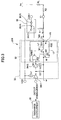
- FIG. 3 is a circuit diagram of an overcurrent protection circuit 200 of a rechargeable battery CELL according to an embodiment of the present invention.
- the overcurrent protection circuit 200 of the rechargeable battery CELL includes a current detection terminal V- and an overcurrent return resistor connecting part 55.
- the overcurrent protection circuit 200 of the rechargeable battery CELL according to the present embodiment may include, as associated structural elements, a discharge control logic circuit containing the overcurrent return resistor connecting part 55, a discharge overcurrent detection circuit 30, a charge control logic circuit 80, a third switching element M3, a charge control terminal COUT, a VDD terminal, a connection terminal P+, and a load RL.
- the overcurrent protection circuit 200 of the rechargeable battery CELL may have a structure and a function to protect the rechargeable battery CELL by detecting an overcharge state, an abnormal charger connection state (a charge overcurrent state), an over discharge state and an output short-circuit state explained above in association with the protection circuit 250 of the rechargeable battery CELL. That is, the overcurrent protection circuit 200 according to the present embodiment may be provided with the over charge detection circuit 10, the over discharge detection circuit 20, the charge overcurrent detection circuit 40, the short-circuit detection circuit 60, the delay circuit 70, the level shift circuit 90, the oscillator 100, and the counter 110 in the rechargeable battery protection integrated circuit, that are illustrated in FIG. 1 .
- the rechargeable battery protection integrated circuit including the overcurrent protection circuit 200 of the rechargeable battery CELL according to the present embodiment may be provided with the VSS terminal connected to a negative electrode of the rechargeable battery CELL, the discharge control terminal DOUT for controlling a discharge of the rechargeable battery CELL, and a delay time reduction terminal DS for reducing a delay time during an inspection.
- the rechargeable battery protection module including the overcurrent protection circuit 200 of the rechargeable battery CELL according to the present embodiment may be provided with the external MOS transistors M11 and M12, the resistors R1 and R2, and the capacitor C1.
- the current detection terminal V- is connected to the negative electrode of the rechargeable battery CELL and the negative electrode of the charger to detect a voltage converted from a charge current and a discharge current of the rechargeable battery CELL.
- a positive voltage is detected at the current detection terminal V-during a discharging operation.
- a negative voltage is detected at the current detection terminal V- during a charging operation.
- the overcurrent protection circuit 200 of the rechargeable battery CELL because the current detection terminal V- performs a protection operation when a discharge overcurrent state is detected, the protection operation is performed when a positive voltage is detected at the current detection terminal V-.
- the external resistor R2 may be connected to the current detection terminal V-, if needed.
- the overcurrent protection circuit of the rechargeable battery CELL according to the present embodiment operates in a state where a discharge overcurrent flows due to the load RL being connected to the connection terminals P+ and P-.
- FIG. 3 illustrates a state where the external resistor R2, the load RL and the connection terminal P+ are connected to the current detection terminal V-.
- the discharge overcurrent detection circuit 30 detects a discharge overcurrent state of the rechargeable battery CELL, when the potential Vd at the current detection terminal V- is equal to or higher than a predetermined discharge overcurrent detection voltage.
- a predetermined discharge overcurrent detection voltage In FIG. 3 , although the current detection terminal V- is not connected to the electric discharge overcurrent detection circuit 30, actually as illustrated in FIG. 1 , the potential detected at the current detection terminal V- is supplied to the discharge overcurrent detection circuit 30. In the discharge overcurrent detection circuit 30, it is determined whether a voltage detected at the current detection terminal V- is equal to or higher than the predetermined discharge overcurrent detection voltage, as mentioned above.
- an overcurrent detection signal is output.
- the discharge control logic circuit 50 includes an overcurrent return resistor connection part 55 (means for connecting an overcurrent return resistor) in order to connect the overcurrent return resistor RS when a discharge overcurrent state is detected by the discharge overcurrent detection circuit 30. Additionally, the discharge control logic circuit 50 may control ON/OFF of the discharge control MOS transistor M12 by controlling a signal output from the discharge control terminal DOUT when a discharge overcurrent state is detected and if the external discharge control MOS transistor M12 (refer to FIG. 1 ) is connected to the discharge control terminal DOUT.
- the discharge control logic circuit 50 includes a current source part including a first current source Is1 and a second current source Is2, an inverter part including a first inverter INV1 and a second inverter INV2, a capacitor C2, and the overcurrent return resistor connection part 55.
- the overcurrent return resistance connection part 55 includes a NAND gate NA, a switching part M including a first switching element M1 and a second switching element M2, and the overcurrent return resistor RS including a first overcurrent return resistor RS1 and a second overcurrent return resistor RS2.
- the inverter part including the first and second inverters INV1 and INV2 may be formed as a CMOS (Complementary Metal Oxide Semiconductor) inverter in which gates and drains of a high potential side P-channel MOS transistor (not illustrated in the figure) and a low potential side N-channel MOS transistor (not illustrated in the figure) are connected with each other.
- the current source part also includes the first and second current sources Is1 and Is2.
- the output from the discharge overcurrent detection circuit 30 is input to the first inverter INV1.
- the first current source Is1 is connected between the P-channel MOS transistor of the first inverter INV1 and the VDD terminal. Thereby, the threshold voltage of the first inverter INV1 can be reduced lower than VDD/2 to change into the threshold potential Vthn of the N-channel MOS transistor.
- the output from the first inverter INV 1 is input to the second inverter INV1.
- the second current source Is2 is connected between the N-channel MOS transistor of the second inverter INV2 and the VSS terminal (GND). Thereby, the threshold voltage of the second inverter INV2 can be changed into the threshold potential Vthp of the second inverter INV2 to set the threshold voltage of the second inverter INV2 higher than VDD/2.
- the overcurrent detection signal detected by the overcurrent detection circuit 30 is inverted while being wave-shaped by the first inverter INV1 and also inverted while being wave-shaped by the second inverter INV2. Accordingly, if the overcurrent detection signal output from the overcurrent detection circuit 30 is at a high level, a high-level signal is output from the second inverter INV2, and if the overcurrent detection signal output from the discharge overcurrent detection circuit 30 is at a low level, a low-level signal is output from the second inverter INV2.
- a description is given of a case where a high-level signal is output from the discharge overcurrent detection circuit 30 and input to the inverter INV1 when a discharge overcurrent state is detected by the discharge overcurrent detection circuit 30.
- the overcurrent return resistance connection part 55 is a means for connecting current detection terminal V- to the overcurrent return resistor part RS, when a discharge overcurrent state is detected by the discharge overcurrent detection circuit 30.
- the overcurrent return resistance connection part 55 includes the overcurrent detection NAND gate NA, the switching means M and the overcurrent return resistor part RS.
- the switching means M includes the first switching element M1 and the second switching element M2.
- the overcurrent return resistor RS also includes the first overcurrent return resistor RS1 and the second overcurrent return resistor RS2.
- the first switching element M1 is directly connected to the first overcurrent return resistor RS1 in series to form a first branch line L1.
- the second switching element M2 is directly connected to the second overcurrent return resistor RS2 in series to form a second branch line L1.
- the first switching element M1 and the second switching element M2 can be any switching element.
- an analog switch or a bipolar switch may be used as the first switching element M1 and the second switching element M2.
- a description will be given of a case where an N-channel MOS transistor is used as the first switching element M1 and the second switching element M2.
- the first switching element M1 may be referred to as a first MOS transistor M1
- the second switching element M2 may be referred to as a second MOS transistor M2.
- the NAND gate NA is a logic operation part having two inputs and one output to perform an AND operation.
- one of the two inputs of the NAND gate NA is referred to as a first input IN1, and the other is referred to as a second input IN2.
- the output of the second inverter INV2 is connected to the second input IN2 and also connected to a gate, which is a switching control input of the second MOS transistor M2. That is, the output signal of the second inverter INV2 is input to the second input IN2 of the NAND gate NA and also input to the gate of the second MOS transistor M2 in order to control ON/OFF of the second MOS transistor M2.
- the first input IN1 of the NAND gate NA is connected to the current detection terminal V- via a third switching element M3.
- the third switching element M3 when the third switching element M3 is ON, the voltage at the current detection terminal V- is input to the first input IN1 of the NAND gate NA.
- an N-channel MOS transistor is used as the third switching element M3 in the present embodiment, other switching elements may be used according to an application.
- the third switching element M3 may be referred to as a third MOS transistor.
- the output of the NAND gate NA is connected to a gate, which is a switching control input of the first MOS transistor M1. That is, the output signal of the NAND gate NA controls ON/OFF of the first MOS transistor M1.
- the first branch line L1 including the first overcurrent return resistor RS1 and the first MOS transistor M1 and the second branch line L2 including the second overcurrent return resistor RS2 and the second MOS transistor M2 are connected by parallel connection to the current detection terminal V-.
- the first MOS transistor M1 is ON
- the first overcurrent return resistor RS1 is connected to the current detection terminal V-.
- the first MOS transistor M1 is OFF
- the first overcurrent return resistor RS1 is disconnected from the current detection terminal V-.
- the second MOS transistor M2 is ON
- the second overcurrent return resistor RS2 is connected to the current detection terminal V-.
- the second MOS transistor M2 is OFF, the second overcurrent return resistor RS2 is disconnected from the current detection terminal V-.
- the first and second overcurrent return resistors RS1 and RS2 in the first and second branch lines L1 and L2 connected to the current detection terminal V-, respectively, and also providing the first and second switching elements M1 and M2 in the first and second branch lines L1 and L2, respectively, the first return resistor RS1 alone, the second return resistor RS2 alone, or both the first and second return resistor RS1 and RS2 in parallel can be selectively connected to the current detection terminal V-.
- the resistance of the first overcurrent return resistor RS1 and the resistance of the second overcurrent return resistor RS2 are set to different values, an appropriate resistance achieved by the overcurrent return resistors RS1 and RS2 can be connected to the current detection terminal V- according to a level of the voltage at the current detection terminal V-.
- the resistance of the first overcurrent return resistor RS1 is set as small as several tens [k ⁇ ] and the resistance of the second overcurrent return resistor RS2 is set as large as from several hundreds [k ⁇ ] to several [M ⁇ ]. The value of the resistances of the first and second return resistor RS1 and RS2 will be explained in detail later.
- the charge control logic circuit 80 determines whether the rechargeable battery CELL is in an over charge state based on a terminal voltage detected at the VDD terminal, and outputs a control signal to the charge control terminal COUT in order to control the charge control MOS transistor M11 when the charge control MOS transistor M11 (refer to FIG. 1 ) is connected externally to the charge control terminal COUT. For example, when the voltage detected at the VDD terminal is higher than a predetermined over charge detection voltage and an over charge state of the rechargeable battery CELL is detected, the charge control logic circuit 80 causes the charge control terminal COUT to output a low-level signal in order to turn off the external charge control MOS transistor M11 to stop a charge operation.
- a high-level signal is always output from the charge control logic circuit 80 to the charge control terminal COUT.
- the control signal of the charge control logic circuit 80 may be output through the level shift circuit 90 such as illustrated in FIG. 1 .
- the charge control logic circuit 80 performs an ON/OFF control of the third switching element M3.
- the control signal output to the charge control terminal COUT is at a high level
- the high-level signal is input to the third MOS transistor M3
- the control signal output to the charge control terminal COUT is at a low level
- the low-level signal is input to the third MOS transistor M3.
- the high-level signal is supplied to the gate of the third MOS transistor M3 because the high-level signal is output from the charge control terminal COUT, thereby maintaining the ON state of the third MOS transistor M3.
- the charge control terminal COUT is outputting a high-level signal because an over charge state never occurs in the discharge overcurrent detection state.
- the third MOS transistor M3 is always in an ON state.
- the input signal to the first input IN1 of the NAND gate NA is at a voltage level of the voltage Vd detected at the current detection terminal V-.
- the output of the NAND gate NA is at a low level because the high-level input signal is input to the first input IN1 and the low-level input signal is input to the second input IN2 of the NAND gate NA.
- the first MOS transistor M1 is turned off and the second MOS transistor M2 is turned on.
- the resistance of the first overcurrent return resistor RS 1 is set to a value, for example, as small as several tens [k ⁇ ] and the resistance of the second overcurrent return resistor RS2 is set to a value, for example, as large as several hundreds [k ⁇ ] to several [M ⁇ ]
- the combined resistance of the overcurrent return resistance can be switched between several tens [k ⁇ ] and several hundreds [k ⁇ ] to several [M ⁇ ].
- the resistance of the overcurrent return resistor RS can be set to several tens [k ⁇ ], and when voltage Vd is larger than the threshold value Vthna of the NAND gate NA, the resistance of the overcurrent return resistor RS can be changed into a resistance value ten times to a thousand times of the resistance value of the overcurrent return resistor RS at the time when the voltage Vd detected at the current detection terminal V-is smaller than the threshold value Vthna of the NAND gate NA.
- the resistance of the overcurrent return resistor RS can be set to a value according to a level of the voltage Vd detected at the current detection terminal, that is, a level of the discharge overcurrent, which permits a great reduction in the leakage current Ileak flowing to the VSS terminal (GND).
- FIG. 4 is a graph indicating a relationship between the voltage Vd detected at the current detection terminal V- and the resistance of the overcurrent return resistor RS in the overcurrent protection circuit 200 of the rechargeable battery CELL according to the present embodiment.
- the horizontal axis represents the value of the voltage Vd detected at the current detection terminal V-
- the vertical axis represents the resistance value of the overcurrent return resistor RS.
- the resistance value of the overcurrent return resistor RS changes from several tens [k ⁇ ] to more than 1.2 [M ⁇ ] according to the value of the voltage Vd at the current detection terminal V-.
- the voltage at which the resistance value of the overcurrent return resistor RS changes is the threshold voltage Vthna of the NAND gate NA. That is, when the voltage Vd at the overcurrent detection terminal V- is equal to or larger than the threshold voltage Vthna of the NAND gate NA, the resistance of the overcurrent return resistor RS is a value as large as 1.2 [M ⁇ ] or larger. On the other hand, when the voltage Vd at the overcurrent detection terminal V- is smaller than the threshold voltage Vthna of the NAND gate NA, the resistance of the overcurrent return resistor RS is as small as several tens [k ⁇ ].
- the leakage current Ileak of the conventional overcurrent protection circuit of a rechargeable battery is about 77 microamperes [ ⁇ A]
- the leakage current Ileak of the overcurrent protection circuit 200 of the rechargeable battery CELL greatly reduces the leakage current Ileak, which provides a long service life of the rechargeable battery CELL.
- the overcurrent return resistor connecting part 55 uses the NAND gate NA in the structure illustrated in FIG. 3
- various modifications may be made for the structure of connection switching.
- various connection methods may be applied to the connection method of the first and second overcurrent return resistors RS1 and RS2.
- various methods may be used if the resistance value of the overcurrent return resistor RS can be changed according to a level of the voltage Vd detected at the current detection terminal V-.
Landscapes
- Engineering & Computer Science (AREA)
- Power Engineering (AREA)
- Physics & Mathematics (AREA)
- General Physics & Mathematics (AREA)
- Manufacturing & Machinery (AREA)
- Chemical & Material Sciences (AREA)
- Chemical Kinetics & Catalysis (AREA)
- Electrochemistry (AREA)
- General Chemical & Material Sciences (AREA)
- Protection Of Static Devices (AREA)
- Charge And Discharge Circuits For Batteries Or The Like (AREA)
- Secondary Cells (AREA)
Applications Claiming Priority (1)
| Application Number | Priority Date | Filing Date | Title |
|---|---|---|---|
| JP2008295744A JP5212042B2 (ja) | 2008-11-19 | 2008-11-19 | 二次電池の過電流保護回路 |
Publications (2)
| Publication Number | Publication Date |
|---|---|
| EP2190100A2 true EP2190100A2 (de) | 2010-05-26 |
| EP2190100A3 EP2190100A3 (de) | 2013-09-04 |
Family
ID=41396268
Family Applications (1)
| Application Number | Title | Priority Date | Filing Date |
|---|---|---|---|
| EP09176014.0A Withdrawn EP2190100A3 (de) | 2008-11-19 | 2009-11-16 | Überstromschutzschaltung einer wiederaufladbaren Batterie |
Country Status (5)
| Country | Link |
|---|---|
| US (1) | US8525482B2 (de) |
| EP (1) | EP2190100A3 (de) |
| JP (1) | JP5212042B2 (de) |
| KR (1) | KR101579596B1 (de) |
| CN (1) | CN101740833B (de) |
Cited By (2)
| Publication number | Priority date | Publication date | Assignee | Title |
|---|---|---|---|---|
| CN101702514A (zh) * | 2009-11-26 | 2010-05-05 | 北京中星微电子有限公司 | 电池保护控制装置 |
| TWI661631B (zh) * | 2014-11-20 | 2019-06-01 | Upi Semiconductor Corp. | 電池保護裝置與其操作方法 |
Families Citing this family (25)
| Publication number | Priority date | Publication date | Assignee | Title |
|---|---|---|---|---|
| US10010336B2 (en) | 2009-12-22 | 2018-07-03 | Cook Medical Technologies, Inc. | Medical devices with detachable pivotable jaws |
| US8545519B2 (en) | 2009-12-22 | 2013-10-01 | Cook Medical Technologies Llc | Medical devices with detachable pivotable jaws |
| US12070224B2 (en) | 2009-12-22 | 2024-08-27 | Cook Medical Technologies Llc | Medical devices with detachable pivotable jaws |
| DK2515770T3 (en) | 2009-12-22 | 2019-02-25 | Cook Medical Technologies Llc | MEDICAL DEVICES WITH REMOVABLE THREADABLE BUYERS |
| US8939997B2 (en) | 2010-10-11 | 2015-01-27 | Cook Medical Technologies Llc | Medical devices with detachable pivotable jaws |
| SI2627268T1 (sl) | 2010-10-11 | 2017-10-30 | Cook Medical Technologies Llc | Medicinske naprave s snemljivimi vrtljivimi čeljustmi |
| DK2627263T3 (en) | 2010-10-11 | 2017-03-06 | Cook Medical Technologies Llc | MEDICAL DEVICES WITH THIRD Jaws |
| EP2651316B1 (de) | 2010-12-15 | 2016-07-06 | Cook Medical Technologies LLC | Medizinische vorrichtungen mit abnehmbaren drehbaren klemmbacken |
| CN102170117B (zh) * | 2011-04-27 | 2014-02-12 | 海能达通信股份有限公司 | 一种电池保护装置及保护方法 |
| JP5715502B2 (ja) * | 2011-06-09 | 2015-05-07 | セイコーインスツル株式会社 | 充放電制御回路及びバッテリ装置 |
| JP5742593B2 (ja) * | 2011-08-30 | 2015-07-01 | ミツミ電機株式会社 | 半導体集積回路、保護回路及び電池パック |
| JP5829966B2 (ja) * | 2012-03-30 | 2015-12-09 | ルネサスエレクトロニクス株式会社 | 電池制御用半導体装置及び電池パック |
| US20140063670A1 (en) * | 2012-09-04 | 2014-03-06 | Samsung Sdi Co., Ltd. | Battery protection circuit and battery pack including the same |
| CN102832669B (zh) * | 2012-09-06 | 2015-10-14 | 深圳市合元科技有限公司 | 电池智能充放电控制电路 |
| JP2014121169A (ja) * | 2012-12-17 | 2014-06-30 | Seiko Instruments Inc | 充放電制御回路及びバッテリ装置 |
| KR101975393B1 (ko) * | 2013-04-18 | 2019-05-07 | 삼성에스디아이 주식회사 | 외장 배터리 |
| JP2015096017A (ja) * | 2013-11-14 | 2015-05-18 | トヨタ自動車株式会社 | 車両およびそれを用いた充放電システム |
| JP6370191B2 (ja) * | 2013-12-11 | 2018-08-08 | エイブリック株式会社 | バッテリ状態監視回路及びバッテリ装置 |
| US10090688B2 (en) * | 2015-01-13 | 2018-10-02 | Intersil Americas LLC | Overcurrent protection in a battery charger |
| CN110365074B (zh) * | 2016-09-20 | 2022-02-11 | 华为技术有限公司 | 一种电池、终端以及充电系统 |
| CN110912212B (zh) * | 2018-09-17 | 2021-07-20 | 硕天科技股份有限公司 | 具适应性限流保护功能的充电装置与手持式电子装置 |
| KR102538990B1 (ko) | 2019-01-24 | 2023-06-01 | 주식회사 엘지에너지솔루션 | 배터리 보호회로 및 이를 이용한 과전류 차단 방법 |
| JP7508454B2 (ja) * | 2019-06-21 | 2024-07-01 | 株式会社半導体エネルギー研究所 | 記憶回路 |
| CN114243806B (zh) * | 2020-09-09 | 2024-05-14 | 高创(苏州)电子有限公司 | 电池充放电控制系统和电子设备 |
| KR20230039565A (ko) * | 2021-09-14 | 2023-03-21 | 에이블릭 가부시키가이샤 | 셀 밸런스 회로, 셀 밸런스 장치, 충방전 제어 회로, 충방전 제어 장치 및 배터리 장치 |
Citations (1)
| Publication number | Priority date | Publication date | Assignee | Title |
|---|---|---|---|---|
| JP2007325434A (ja) | 2006-06-01 | 2007-12-13 | Ricoh Co Ltd | 充放電保護回路、該充放電保護回路を組み込んだバッテリーパック、該バッテリーパックを用いた電子機器 |
Family Cites Families (12)
| Publication number | Priority date | Publication date | Assignee | Title |
|---|---|---|---|---|
| US6031358A (en) * | 1998-07-02 | 2000-02-29 | Sony Corporation | Short protection circuit for rechargable battery |
| JP2000194456A (ja) * | 1998-12-25 | 2000-07-14 | Matsushita Electric Ind Co Ltd | バッテリ―監視装置 |
| TW468295B (en) * | 1999-04-15 | 2001-12-11 | Seiko Instr Inc | Charge/discharge controlling semiconductor device |
| US6798175B2 (en) | 2000-04-11 | 2004-09-28 | Pentax Corporation | Power supply circuit |
| US6501248B2 (en) | 2000-09-28 | 2002-12-31 | Ricoh Company, Ltd. | Charge/discharge protection apparatus having a charge-state overcurrent detector, and battery pack including the same |
| US6809553B2 (en) * | 2001-10-15 | 2004-10-26 | International Rectifier Corporation | Digital level shifter with reduced power dissipation and false transmission blocking |
| JP4619812B2 (ja) * | 2005-02-16 | 2011-01-26 | 株式会社東芝 | ゲート駆動回路 |
| JP4415131B2 (ja) * | 2005-10-31 | 2010-02-17 | ミツミ電機株式会社 | 電池保護装置及び電池保護回路 |
| JP4407641B2 (ja) * | 2006-01-16 | 2010-02-03 | ソニー株式会社 | 2次電池装置 |
| US7584370B2 (en) * | 2006-06-22 | 2009-09-01 | Skyworks Solutions, Inc. | Circuits, switch assemblies, and methods for power management in an interface that maintains respective voltage differences between terminals of semiconductor devices in open and close switch states and over a range of voltages |
| JP2008118828A (ja) * | 2006-11-08 | 2008-05-22 | Meidensha Corp | 電気二重層キャパシタ充電装置 |
| JP4752811B2 (ja) * | 2007-06-06 | 2011-08-17 | 日産自動車株式会社 | 電圧駆動型素子の駆動回路 |
-
2008
- 2008-11-19 JP JP2008295744A patent/JP5212042B2/ja active Active
-
2009
- 2009-09-24 KR KR1020090090368A patent/KR101579596B1/ko active Active
- 2009-11-13 US US12/617,755 patent/US8525482B2/en active Active
- 2009-11-16 EP EP09176014.0A patent/EP2190100A3/de not_active Withdrawn
- 2009-11-17 CN CN200910222731.XA patent/CN101740833B/zh active Active
Patent Citations (1)
| Publication number | Priority date | Publication date | Assignee | Title |
|---|---|---|---|---|
| JP2007325434A (ja) | 2006-06-01 | 2007-12-13 | Ricoh Co Ltd | 充放電保護回路、該充放電保護回路を組み込んだバッテリーパック、該バッテリーパックを用いた電子機器 |
Cited By (3)
| Publication number | Priority date | Publication date | Assignee | Title |
|---|---|---|---|---|
| CN101702514A (zh) * | 2009-11-26 | 2010-05-05 | 北京中星微电子有限公司 | 电池保护控制装置 |
| CN101702514B (zh) * | 2009-11-26 | 2014-09-10 | 北京中星微电子有限公司 | 电池保护控制装置 |
| TWI661631B (zh) * | 2014-11-20 | 2019-06-01 | Upi Semiconductor Corp. | 電池保護裝置與其操作方法 |
Also Published As
| Publication number | Publication date |
|---|---|
| CN101740833B (zh) | 2015-03-25 |
| EP2190100A3 (de) | 2013-09-04 |
| US8525482B2 (en) | 2013-09-03 |
| CN101740833A (zh) | 2010-06-16 |
| US20100123437A1 (en) | 2010-05-20 |
| KR20100056362A (ko) | 2010-05-27 |
| JP5212042B2 (ja) | 2013-06-19 |
| JP2010124600A (ja) | 2010-06-03 |
| KR101579596B1 (ko) | 2015-12-22 |
Similar Documents
| Publication | Publication Date | Title |
|---|---|---|
| EP2190100A2 (de) | Überstromschutzschaltung einer wiederaufladbaren Batterie | |
| JP5439800B2 (ja) | 二次電池保護用集積回路装置及びこれを用いた二次電池保護モジュール並びに電池パック | |
| US6316915B1 (en) | Charge/discharge protection circuit and battery pack having the charge/discharge protection circuit | |
| CN108242832B (zh) | 充电控制电路、电池保护集成电路、电池组及电池系统 | |
| JP5718478B2 (ja) | リチウム電池保護回路 | |
| US10749358B2 (en) | Rechargeable battery protection integrated circuit, rechargeable battery protection device, and battery pack | |
| TWI580154B (zh) | 充放電控制電路及電池裝置 | |
| JP7235987B2 (ja) | 二次電池保護回路及び電池パック | |
| JPH07131938A (ja) | 充放電制御回路と充電式電源装置 | |
| US20020109486A1 (en) | Power source circuit | |
| CN1988315A (zh) | 电池装置 | |
| JP4297452B2 (ja) | 充放電保護回路 | |
| JP3434760B2 (ja) | 充放電制御回路と充電式電源装置 | |
| CN108258751B (zh) | 充放电控制电路以及电池装置 | |
| KR102785018B1 (ko) | 이차전지 보호 회로, 전지 팩, 전지 시스템 및 이차전지 보호 방법 | |
| JP3434759B2 (ja) | 充放電制御回路と充電式電源装置 | |
| JP2023147174A (ja) | 電圧検出回路、充電制御回路、充放電制御回路及び半導体装置 | |
| US12620820B2 (en) | Secondary battery protection circuit, battery pack, battery system, and method for protecting secondary battery | |
| EP4270723B1 (de) | Spannungsdetektionsschaltung, ladungssteuerungsschaltung, ladungs- und entladungssteuerungsschaltung und halbleiterbauelement | |
| JP2006121900A (ja) | 充放電保護回路および該充放電保護回路を有するバッテリーパック | |
| CN116930598A (zh) | 电压检测电路、充电及充放电控制电路以及半导体装置 | |
| JP2003061252A (ja) | 充放電制御回路と充電式電源装置 |
Legal Events
| Date | Code | Title | Description |
|---|---|---|---|
| PUAI | Public reference made under article 153(3) epc to a published international application that has entered the european phase |
Free format text: ORIGINAL CODE: 0009012 |
|
| AK | Designated contracting states |
Kind code of ref document: A2 Designated state(s): AT BE BG CH CY CZ DE DK EE ES FI FR GB GR HR HU IE IS IT LI LT LU LV MC MK MT NL NO PL PT RO SE SI SK SM TR |
|
| AX | Request for extension of the european patent |
Extension state: AL BA RS |
|
| PUAL | Search report despatched |
Free format text: ORIGINAL CODE: 0009013 |
|
| AK | Designated contracting states |
Kind code of ref document: A3 Designated state(s): AT BE BG CH CY CZ DE DK EE ES FI FR GB GR HR HU IE IS IT LI LT LU LV MC MK MT NL NO PL PT RO SE SI SK SM TR |
|
| AX | Request for extension of the european patent |
Extension state: AL BA RS |
|
| RIC1 | Information provided on ipc code assigned before grant |
Ipc: H02J 7/00 20060101AFI20130801BHEP |
|
| STAA | Information on the status of an ep patent application or granted ep patent |
Free format text: STATUS: THE APPLICATION IS DEEMED TO BE WITHDRAWN |
|
| 18D | Application deemed to be withdrawn |
Effective date: 20140305 |