EP2192687A2 - Amplificateur et commutation d'amplification dotée d'une capacité commutée - Google Patents
Amplificateur et commutation d'amplification dotée d'une capacité commutée Download PDFInfo
- Publication number
- EP2192687A2 EP2192687A2 EP09014521A EP09014521A EP2192687A2 EP 2192687 A2 EP2192687 A2 EP 2192687A2 EP 09014521 A EP09014521 A EP 09014521A EP 09014521 A EP09014521 A EP 09014521A EP 2192687 A2 EP2192687 A2 EP 2192687A2
- Authority
- EP
- European Patent Office
- Prior art keywords
- amplifier
- compensation
- switch
- frequency compensation
- capacity
- Prior art date
- Legal status (The legal status is an assumption and is not a legal conclusion. Google has not performed a legal analysis and makes no representation as to the accuracy of the status listed.)
- Granted
Links
- 238000000034 method Methods 0.000 claims abstract description 4
- 239000003990 capacitor Substances 0.000 claims description 58
- 238000011144 upstream manufacturing Methods 0.000 claims description 13
- 101100260207 Schizosaccharomyces pombe (strain 972 / ATCC 24843) sfc2 gene Proteins 0.000 claims description 4
- 230000000694 effects Effects 0.000 claims description 4
- 101100113692 Caenorhabditis elegans clk-2 gene Proteins 0.000 claims description 3
- 230000003321 amplification Effects 0.000 description 6
- 238000003199 nucleic acid amplification method Methods 0.000 description 6
- 230000001052 transient effect Effects 0.000 description 4
- 238000005457 optimization Methods 0.000 description 2
- 230000003071 parasitic effect Effects 0.000 description 2
- 230000001960 triggered effect Effects 0.000 description 2
- 238000010276 construction Methods 0.000 description 1
- 230000001419 dependent effect Effects 0.000 description 1
- 238000005516 engineering process Methods 0.000 description 1
- 239000004065 semiconductor Substances 0.000 description 1
Images
Classifications
-
- H—ELECTRICITY
- H03—ELECTRONIC CIRCUITRY
- H03F—AMPLIFIERS
- H03F1/00—Details of amplifiers with only discharge tubes, only semiconductor devices or only unspecified devices as amplifying elements
- H03F1/42—Modifications of amplifiers to extend the bandwidth
Definitions
- the invention relates to an amplifier for a switched capacitor amplifier circuit having the above-mentioned features according to claim 1 or to such a switched capacitor amplifier circuit and such an amplifier.
- Switched capacitor circuits are used as amplifiers in many applications.
- An example is a use in a so-called pipeline analog-to-digital converter.
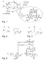
- Fig. 1 shows in the left, not shown enlarged figure portion a particular form of an amplifier arrangement with an amplifier circuit IC.
- the amplifier arrangement is designed with switched capacitance Cf, Cs and is also referred to below as a switched capacitor amplifier.
- reset configuration English reset / German: reset
- problems can be avoided by an offset (German: offset) of an amplifier used therein V, since this offset in a first clock phase ⁇ 1 of two clock phases ⁇ 1, ⁇ 2 (English Clockphases) is stored and not in a second of the clock phases ⁇ 2 more than mistakes appear.
- a circuit input i to which an input voltage Vi is applied, leads to a first switch S1 and a second switch S2 connected in parallel therewith. These two switches S1, S2 can be driven to close by a first switching signal, which is applied in a first clock phase ⁇ 1.
- a first switchable capacitance Cs switched between the second switch S2 and the amplifier input node n.
- a negative set input of the amplifier V * is connected between the amplifier input node n and a circuit output node o. At the amplifier output node o results in an output voltage Vo.
- a positive input of the amplifier V is connected to a ground terminal or to a reference potential GND.
- the amplifier input node n is switchable via a third switch S3 parallel to the amplifier V to the amplifier output node o.
- the first switching signal ⁇ 1 can also be applied to it.
- a control voltage in the form of, for example, a digital / analog converter output voltage Vdac or another reference potential, such as a reference voltage Vcm can be applied to a node between the first switch S1 and the second switchable capacitance Cs via a fifth switch S5.
- a fifth switch S5 For the closing switching of the fifth switch S5 is a second switching signal, which is applied in the second clock phase ⁇ 2.
- a fourth switch S4 which is likewise triggered by means of the second switching signal, a node between the second switch S2 and the first switchable capacitance Cf is connectable to the amplifier output node o.
- control device X which is designed, inter alia, to provide the first and the second switching signal in the first and second clock phase ⁇ 1, ⁇ 2.
- the control takes place in a known manner.
- Fig. 2 outlines the capacitors and their capacitances CS and CF in parallel switched and by means of the first two in Fig. 1 outlined switches S1 and S2 connected to the circuit input i.
- the amplifier V is completely fed back by means of the third switch S3.
- the output voltage Vo and thus the voltage at the second node of the two capacitances Cs & Cf is the reference voltage Vcm, which is also referred to as common mode voltage plus the offset voltage Voff of the amplifier V.
- Vcm which is also referred to as common mode voltage plus the offset voltage Voff of the amplifier V.
- Fig. 3 outlines the first two first in Fig. 1 sketched switches S1 and S2 open.
- the fifth switch S5 is closed and connects the second switchable capacitance Cs with the reference voltage Vcm at a switched capacitor amplifier or with a digital / analogue converter output voltage Vdac in a pipeline analog-to-digital converter.
- the full feedback of the amplifier V is canceled because the third switch S3 is opened, and the first switchable capacitance Cf is connected to the output node o by means of the closed fourth switch S4 from the amplifier input node n of the amplifier V.
- the output voltage Vo in the second clock phase ⁇ 2 is thus compensated for by the amplified, negative input voltage Vi in the first clock phase ⁇ 1 , the offset voltage Voff.
- the amplification error Aerr becomes smaller the greater the gain A0 of the amplifier V is.
- OTA circuits i. Transconductance amplifier or current amplifier with operational amplification, used in conjunction with cascode circuits.
- the gain V0 can be further increased by using gain boosting circuits.
- the advantage of the one-stage arrangements is that high bandwidths are achieved, since additional measures for frequency compensation are not required.
- Fig. 6 shows a possible two-stage amplification arrangement of a frequency compensated amplifier V *.
- the compensation input node n2 Between the two amplifier stages V1, V2 there is a node, which is referred to below as the compensation input node n2.
- a first amplifier capacitance C1 and a first further resistor Ro1 are connected in parallel with one another.
- a load capacitance CL and a second further resistance Ro2 are connected in parallel with each other.
- the first amplifier capacitance C1 and the first further resistor Ro1 can already be formed by device properties.
- the first additional resistor Ro1 is the output resistance of the upstream amplifier stage V1 as the source of the real transconductance gm1
- the first amplifier capacitance C1 is the input capacitance of the second amplifier stage V2 with its transconductance gm2 and the parasitic load capacitance of the output of the upstream amplifier stage V1.
- An explicit placement of a first further resistor Ro1 or the first amplifier capacitance C1 does not have to, but can take place. Accordingly, if necessary, the existing parasitic elements are sufficient.
- a first compensation resistor RZ and a capacitance or total capacity for frequency compensation CC are connected in series between the compensation input node n2 and the amplifier output node o.
- the amplifier V * is only fed back to a smaller extent.
- Frequency compensation for multistage amplifiers must be designed in such a way that there is a stable control system in both clock phases ⁇ 1, ⁇ 2. Due to the larger feedback factor ⁇ ( ⁇ 1) during the first clock phase ⁇ 1, this phase is the decisive phase for the frequency compensation.
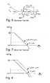
- Fig. 6 illustrates a possible frequency compensation for a second order amplification system, a so-called Miller compensation.
- ⁇ 1
- CL load capacitance
- g m1 and g m2 of the two amplifier stages V1, V2 a certain transit frequency f T , as can be seen from eg PE Allan, DR Holberg; CMOS analog circuit design; Oxford University Press; , 1987; ISBN 0-19-510720-9; page 374ff ; Section 8.2 etc. is known.
- the feedback factor ⁇ may be considerably lower.
- the feedback factor ⁇ is only 1/2.
- the gain bandwidth product GBW is constant and must be designed for the first clock phase ⁇ 1 .
- the bandwidth of the feedback amplifier V * during the second clock phase ⁇ 2 is thus only half as large as during the first clock phase ⁇ 1. This leads to a longer settling time, which can only be avoided by a higher bandwidth in the first clock phase ⁇ 1 and thus by a higher current consumption.
- the object of the invention is to provide a switched capacitor amplifier circuit having improved circuit construction.
- a disadvantage of a bandwidth reduction of the system during the second clock phase should be avoided without increasing the power consumption.
- an amplifier for a switched capacitor amplifier circuit wherein a capacitor for frequency compensation is connected in parallel to an amplifier stage and wherein at least a second capacitor for frequency compensation by means of a capacitance switching signal and / or a compensation switch or switched parallel to this first Capacitance for frequency compensation is switched.
- the amplifier is constructed such that the gain bandwidth product is no longer equal during the two clock phases or GBW ( ⁇ 1) ⁇ GBW ( ⁇ 2) holds.
- a resistor is preferably an ohmic Resistance understood.
- a capacity is understood to mean a component which has a capacitive effect, in particular a capacitor.
- a switch is turned on or off.
- a switch can be understood as any form of switch, in particular transistors or other semiconductor structures with a corresponding switching function.
- the compensation switch preferably has a switch resistance greater than zero, which, when switched on, effects a series connection of a resistor, in particular an ohmic resistor, to the second capacitor for frequency compensation.
- a resistor in particular an ohmic resistor
- the switch resistor corresponds in particular to a so-called nulling resistor or a part thereof.
- a combination for the nulling resistor which consists of the so-called on-resistance of the switch and of another, explicitly placed resistor.
- a compensation resistor is connected in series with the non-switched first capacitor for frequency compensation.
- the compensation resistor may be formed by a switch.
- the compensation resistor is formed by further and closed switch with parameters of the compensation switch, wherein the further compensation switch is not switched or is not switchable.
- Such a dummy switch in series with a non-switched first capacity for frequency compensation is advantageous as a "nulling resistor" to improve of matching with the other, switched second capacity to achieve frequency compensation.
- the first capacitance for frequency compensation and the at least one second capacitance or the frequency compensation or the compensation switch can be connected to an input of the amplifier stage and connected to an output of an amplifier stage connected upstream thereto and to the amplifier stage in parallel a third capacitance for frequency compensation, in which case a fourth capacity for frequency compensation by means of a further capacitance switching signal and / or a further compensation switch on or switched off parallel to this third capacitance for frequency compensation is connected.
- a bias voltage is switched between on the one hand the input of the amplifier stage, the connection of the first capacitor for frequency compensation thereto and the connection of the at least second capacitor or the compensation switch thereto and, on the other hand, the output of the upstream amplifier stage, the connection of the third capacitor for frequency compensation thereto and connecting the fourth frequency compensation capacitor or the other compensation switch thereto.
- this makes possible a switchable frequency compensation capacity in switch capacitor amplifiers in reset configuration for the independent optimization of the transient response in the two different clock phases by adding additional capacitances during one, in particular first clock phase with a switch.
- the compensation switch is preferably closed during the first clock phase and the first capacitance for frequency compensation switches in parallel to the second capacitance for frequency compensation.
- the compensation switch is accordingly opened during the second clock phase and the first capacity for frequency compensation is switched off.
- the compensation switch is preferably closed during the first clock phase and the first capacitance for frequency compensation is connected in parallel with the second capacitance for frequency compensation. Accordingly, the compensation switch is opened during the second clock phase and the first capacity for frequency compensation switched off.
- a switchable frequency compensation capacity in switch capacitor amplifiers in reset configuration is made possible for the independent optimization of the transient response in the two different clock phases by adding additional capacitances during the one, in particular first, clock phase with a switch.
- Fig. 1 illustrates in the right section enlargement a particularly preferred possibility of realizing a suitable amplifier.
- a circuit input i to which an input voltage Vi is applied, leads to a first switch S1 and a second switch S2 connected in parallel therewith. These two switches S1, S2 can be driven to close by a first switching signal, which is applied in a first clock phase ⁇ 1.
- a second switchable capacitance Cs is connected in series.
- a first switchable capacitance Cf is connected between the second switch S2 and the amplifier input node n.
- a negative set input of the amplifier V * is connected between the amplifier input node n and a circuit output node o. At the amplifier output node o correspondingly results in an output voltage Vo.
- a positive input of the amplifier V is connected to a ground terminal or to a reference potential GND.
- the amplifier input node n is switchable via a third switch S3 parallel to the amplifier V to the amplifier output node o.
- the first switching signal ⁇ 1 can be applied for the closing switching of the third switch S3 to this.
- a control voltage in the form of, for example, a digital / analog converter output voltage Vdac can be applied to a node between the first switch S1 and the second switchable capacitance Cs via a fifth switch S5.
- a fifth switch S5 For the closing switching of the fifth switch S5 is a second switching signal, which is applied in the second clock phase ⁇ 2.
- a fourth switch S4 which is likewise triggered by means of the second switching signal, a node between the second switch S2 and the first switchable capacitance Cf is connectable to the amplifier output node o.
- control device X which is designed, inter alia, to provide the first and the second switching signal in the first and second clock phase ⁇ 1, ⁇ 2.
- the control takes place in a known manner. The operation corresponds essentially, as well as the structure of the description of the prior art.
- the compensation input node n2 Between the two amplifier stages V1, V2 there is a node, which is referred to below as the compensation input node n2.
- a first amplifier capacitance C1 and a first further resistor Ro1 are connected in parallel with one another.
- a load capacitance CL and a second further resistor Ro2 are connected in parallel with each other.
- total capacity for frequency compensation CC is in the preferred embodiment according to Fig. 1 used a capacity with a lower capacity value.
- This thus forms a first capacitor for frequency compensation CC1, which is connected in series with the first compensation resistor RZ between the compensation input node n2 and the amplifier output node o.
- a compensation switch SFC and a second capacitor for frequency compensation CC2 are connected in series between the compensation input node n2 and the amplifier output node o.
- the capacitance values of the first and second frequency compensation capacitors CC1, CC2 are chosen to have the same effect as the total capacitance when the compensation switch SFC is closed.
- the compensation switch SFC is actuated to close by a capacitance switching signal clk, which is likewise provided by the control device X.
- the capacitance switching signal clk is preferably controlled inversely to the control signal of the second clock phase ⁇ 2 or equal to the switching signal of the first clock phase ⁇ 1.
- an even further ohmic resistor can be connected in series with the compensation switch SFC and the second capacitor for frequency compensation CC2.
- the compensation switch SFC has a suitable resistance value is preferred.
- CC for frequency compensation is thus according to the preferred embodiment in Fig. 1 divided into two capacitances, a first and a second divided capacity for frequency compensation CC1 and CC2.
- the compensation switch SFC is open, and only the first shared frequency compensation capacitor CC1 is effective for frequency compensation.
- This is for optimal transient response of the system during the second Clock phase ⁇ 2 suitably set, in particular to optimize and is thus a function of the feedback factor ⁇ ( ⁇ 2) and the load capacitance CL ( ⁇ 2) during the second clock phase ⁇ 2.
- the feedback factor ⁇ ( ⁇ 1) is greater than the feedback factor ⁇ ( ⁇ 2) during the second clock phase ⁇ 2, i. we have ⁇ ( ⁇ 1)> ⁇ ( ⁇ 2).
- the value of the first amplifier capacitance C1 is to be set independently of the value of the first switchable capacitance CF, in particular to be optimized in order to take into account an influence of different load capacitances, etc., and in practice is not necessarily equal to the value of the first switchable capacitance CF.
- Amplifier V surrounding circuit components thus, a control technology stable system is achieved both in the first clock phase ⁇ 1 and in the second clock phase ⁇ 2 without increasing the power consumption.
- each of the divided capacitance-sharing capacitors CC1, CC2 can preferably be switched over between the two clock phases ⁇ 1 and ⁇ 2.
- the compensation capacitance from the first and the second divided capacitance frequency compensation capacitors CC1, CC2 is connected in series with a resistor as a compensation resistor RZ.
- a further improvement of the frequency compensation can be achieved by the use of various such resistance-capacitance series circuits in the two clock phases ⁇ 1 and ⁇ 2.
- the resistance of the closed compensation switch SFC itself can be used in whole or in part as a series resistor or as a compensation resistor in series with the second divided capacitor for frequency compensation CC2. If the switch SFC itself is used as a compensation resistor, it is advantageous to replace the first compensation resistor RZ in the compensation branch, which is active only during the second clock phase ⁇ 2, also by a switch. This achieves particularly good matching between the two clock phases ⁇ 1, ⁇ 2.
- Such an arrangement is applicable to so-called single-ended as well as fully differential amplifier circuits.
- Fig. 1 are generally slopes gm1 or gm2 described. So that the arrangement in Fig. 1 is working, the gain of the second stage, namely the product of the values of the slope gm2 and the second further resistance Ro2 itself is of course negative. So the slope gm2 of the amplifier stage V2 is negative. Mathematically, this is correct since the slope gm2 is not limited to positive values.
- a dummy switch in series with a non-switched second frequency compensation capacitor CC2 as "nulling resistor” is advantageous in order to achieve an improvement of the matching with the other, first switched capacitor CC1.
- Fig. 5 shows an exemplary modified embodiment for forming a so-called nested cascode miller OpAmp, wherein hereinafter essentially only different features for the embodiment according to Fig. 1 to be discribed.
- the first capacitor for frequency compensation CC1 and the at least one second capacitor or for the frequency compensation CC2 or the compensation switch SFC are connected with their one end back to an input n3 of the amplifier stage V2.
- a third capacitor for frequency compensation CC3 is connected in parallel with an output n4 of the amplifier stage V1 connected upstream thereof and with the amplifier stage V2 in parallel.
- a fourth capacity for frequency compensation CC4 can be switched on or off parallel to this by means of a further capacitance switching signal clk2 and / or a further compensation switch SFC2 third capacitor for frequency compensation CC3 and connected to the output n4.
- the third and fourth capacitances are connected in parallel to the first and second capacitances.
- a further stage is connected, which operates as a cascode for the first amplifier stage V1 and whose transconductance gm1.
- This further, working as a cascode stage is exemplified with a MOSFET. From the MOSFET whose source terminal is connected to the node or at the output n4 of the upstream amplifier stage V1, whose drain terminal connected to the accounts or input n3 of the amplifier stage V2 and the gate terminal connected to a further reference potential Vbias.
- a Miller-compensated amplifier according to Fig. 1 in the simplest case it is just a capacity.
- further embodiments in which even more or all capacitors involved in a frequency compensation are designed to be switchable can also be implemented according to this basic principle. However, it does not matter if all of these capacities are actually switched or only one, which is sufficient for most applications.
- Fig. 1 only one capacity is used. If a fully differential amplifier is used, there are also two capacitances that can be switched, even in a simple arrangement.
Landscapes
- Engineering & Computer Science (AREA)
- Power Engineering (AREA)
- Amplifiers (AREA)
Applications Claiming Priority (1)
| Application Number | Priority Date | Filing Date | Title |
|---|---|---|---|
| DE102008059734A DE102008059734A1 (de) | 2008-12-01 | 2008-12-01 | Verstärker und Verstärkerschaltung mit geschalteter Kapazität |
Publications (3)
| Publication Number | Publication Date |
|---|---|
| EP2192687A2 true EP2192687A2 (fr) | 2010-06-02 |
| EP2192687A3 EP2192687A3 (fr) | 2010-06-16 |
| EP2192687B1 EP2192687B1 (fr) | 2014-03-19 |
Family
ID=41647126
Family Applications (1)
| Application Number | Title | Priority Date | Filing Date |
|---|---|---|---|
| EP09014521.0A Not-in-force EP2192687B1 (fr) | 2008-12-01 | 2009-11-20 | Amplificateur et commutation d'amplification dotée d'une capacité commutée |
Country Status (3)
| Country | Link |
|---|---|
| US (1) | US8193856B2 (fr) |
| EP (1) | EP2192687B1 (fr) |
| DE (1) | DE102008059734A1 (fr) |
Cited By (1)
| Publication number | Priority date | Publication date | Assignee | Title |
|---|---|---|---|---|
| CN109324210A (zh) * | 2018-12-13 | 2019-02-12 | 江苏集萃微纳自动化系统与装备技术研究所有限公司 | 补偿控制器及mems加速度计闭环伺服专用集成电路 |
Families Citing this family (4)
| Publication number | Priority date | Publication date | Assignee | Title |
|---|---|---|---|---|
| DE112015005942B4 (de) * | 2015-01-13 | 2026-04-02 | Sumitomo Riko Company Limited | Kapazitätsmessvorrichtung, kapazitätstypartige Flachsensoreinrichtung und kapazitätstypartige Flüssigkeitspegeldetektionseinrichtung |
| US10044327B2 (en) | 2016-09-09 | 2018-08-07 | Analog Devices Global | Fast settling capacitive gain amplifier circuit |
| EP3729657B1 (fr) * | 2017-12-22 | 2022-03-02 | Telefonaktiebolaget Lm Ericsson (Publ) | Convertisseur analogique-numérique (can) à entrelacement temporel |
| US12438509B2 (en) * | 2023-06-16 | 2025-10-07 | Trustees Of Boston University | Extended energy range particle detectors and uses thereof |
Family Cites Families (15)
| Publication number | Priority date | Publication date | Assignee | Title |
|---|---|---|---|---|
| US3153202A (en) * | 1961-05-12 | 1964-10-13 | Gen Electric | Direct-coupled amplifier |
| JPS59224906A (ja) * | 1983-06-03 | 1984-12-17 | Hitachi Ltd | チヨツパ形増幅回路 |
| JPS60128702A (ja) * | 1983-12-16 | 1985-07-09 | Hitachi Ltd | 半導体集積回路装置 |
| US4543534A (en) * | 1984-05-04 | 1985-09-24 | The Regeants Of University Of Calif. | Offset compensated switched capacitor circuits |
| IT1213243B (it) * | 1984-11-12 | 1989-12-14 | Ates Componenti Elettron | Circuito buffer a struttura differenziale per la misurazione di cariche capacitive. |
| US5363055A (en) * | 1993-03-15 | 1994-11-08 | General Electric Company | Photodiode preamplifier with programmable gain amplification |
| DE69529828D1 (de) * | 1995-11-30 | 2003-04-10 | St Microelectronics Srl | Operationsverstärker mit steuerbarer Frequenzkompensation |
| JP3079368B2 (ja) * | 1997-10-24 | 2000-08-21 | セイコーインスツルメンツ株式会社 | スイッチトキャパシタ増幅回路 |
| US5999042A (en) * | 1998-03-30 | 1999-12-07 | Plasmon Lms, Inc. | Switchable response active filter |
| DE10031522B9 (de) | 2000-06-28 | 2007-07-12 | Infineon Technologies Ag | Frequenzkompensierte Verstärkeranordnung und Verfahren zum Betrieb einer frequenzkompensierten Verstärkeranordnung |
| JP3737346B2 (ja) * | 2000-08-28 | 2006-01-18 | シャープ株式会社 | サンプルホールド増幅回路とそれを用いたパイプライン型ad変換器およびパイプライン型da変換器 |
| US6400301B1 (en) * | 2000-09-07 | 2002-06-04 | Texas Instruments Incorporated | amplifying signals in switched capacitor environments |
| US20020153946A1 (en) * | 2001-04-23 | 2002-10-24 | Nguyen Khiem Quang | Dynamic frequency compensated operation amplifier |
| DE10251308B4 (de) * | 2002-11-04 | 2007-01-18 | Advanced Micro Devices, Inc., Sunnyvale | Integrierte geschaltete Kondensatorschaltung und Verfahren |
| KR100674912B1 (ko) * | 2004-09-24 | 2007-01-26 | 삼성전자주식회사 | 슬루 레이트(slew rate)를 개선시킨 차동 증폭회로 |
-
2008
- 2008-12-01 DE DE102008059734A patent/DE102008059734A1/de not_active Withdrawn
-
2009
- 2009-11-20 EP EP09014521.0A patent/EP2192687B1/fr not_active Not-in-force
- 2009-12-01 US US12/628,748 patent/US8193856B2/en not_active Expired - Fee Related
Non-Patent Citations (1)
| Title |
|---|
| P.E. ALLAN; D.R. HOLBERG: "CMOS Analog Circuit Design", 1987, OXFORD UNIVERSITY PRESS, pages: 374 |
Cited By (2)
| Publication number | Priority date | Publication date | Assignee | Title |
|---|---|---|---|---|
| CN109324210A (zh) * | 2018-12-13 | 2019-02-12 | 江苏集萃微纳自动化系统与装备技术研究所有限公司 | 补偿控制器及mems加速度计闭环伺服专用集成电路 |
| CN109324210B (zh) * | 2018-12-13 | 2024-03-15 | 江苏集萃微纳自动化系统与装备技术研究所有限公司 | 补偿控制器及mems加速度计闭环伺服专用集成电路 |
Also Published As
| Publication number | Publication date |
|---|---|
| DE102008059734A1 (de) | 2010-06-02 |
| EP2192687A3 (fr) | 2010-06-16 |
| US20100171551A1 (en) | 2010-07-08 |
| US8193856B2 (en) | 2012-06-05 |
| EP2192687B1 (fr) | 2014-03-19 |
Similar Documents
| Publication | Publication Date | Title |
|---|---|---|
| DE112016000891B4 (de) | Differenzielle geschaltete Kondensatorschaltungen mit Spannungsverstärkern, und dazugehörige Verfahren | |
| DE3631099C2 (de) | CMOS Ausgangsstufe | |
| EP1997227B1 (fr) | Dispositif de commutation et procédé de préparation d'un signal d'horloge avec un rapport impulsion/pause réglable | |
| DE102014102456A1 (de) | Ein verstärker, ein restverstärker und ein a/d-wandler, der einen restverstärker aufweist | |
| DE102004052174B4 (de) | Verstärkerschaltung, umfassend einen Verstärker mit tiefpassgefilterter Rückkopplung | |
| EP2192687B1 (fr) | Amplificateur et commutation d'amplification dotée d'une capacité commutée | |
| DE102018101177A1 (de) | Schaltung mit geschalteten Kondensatoren und Verfahren zum Betreiben einer Schaltung mit geschalteten Kondensatoren | |
| DE3017669A1 (de) | Regelverstaerker | |
| DE2314015C3 (de) | Signalverstärker | |
| DE10042170A1 (de) | Differentieller, komplementärer Verstärker | |
| DE60028287T2 (de) | Leitungstreiberverstärker mit verteilter Verstärkung | |
| DE102010035276B4 (de) | Verfahren zur Offsetkompensation eines Switched Capacitor-Verstärkers und Switched Capacitor-Verstärkeranordnung | |
| EP1545000B1 (fr) | Circuit pour réguler le rapport cyclique d'un signal électrique | |
| DE10054540B4 (de) | Verstärkerschaltung, insbesondere Leitungstreiber und Verfahren zur Verstärkung eines Signals, insbesondere Verfahren zum Treiben eines Leitungssignals | |
| DE102004022991B3 (de) | Abtast-Differenzverstärker und Abtast-Verstärker | |
| DE1537656B2 (fr) | ||
| DE112021004914T5 (de) | Differenzverstärkeranordnung und konverteranordnung | |
| DE102017120420B4 (de) | Schnell einschwingende kapazitive gain-verstärkerschaltung | |
| EP1844382B1 (fr) | Circuit de filtrage | |
| DE102005008099B4 (de) | Filter-Schaltungsanordnung höherer Ordnung | |
| DE102010028037B4 (de) | Switched-Capacitor-Integrator mit Ladungsrückkopplung zur Erhöhung der Eingangsimpedanz | |
| EP1254512B1 (fr) | Circuit amplificateur ou filtre a capacites commutees et procede d'amplification ou de filtrage de signaux | |
| DE102008034324B4 (de) | Verstärkerschaltung | |
| DE2440937B2 (de) | Differenzverstaerker mit zwei mos- transistoren | |
| DE10040399A1 (de) | Schaltbarer Operationsverstärker für Switched-Opamp-Anwendungen |
Legal Events
| Date | Code | Title | Description |
|---|---|---|---|
| PUAI | Public reference made under article 153(3) epc to a published international application that has entered the european phase |
Free format text: ORIGINAL CODE: 0009012 |
|
| PUAL | Search report despatched |
Free format text: ORIGINAL CODE: 0009013 |
|
| AK | Designated contracting states |
Kind code of ref document: A2 Designated state(s): AT BE BG CH CY CZ DE DK EE ES FI FR GB GR HR HU IE IS IT LI LT LU LV MC MK MT NL NO PL PT RO SE SI SK SM TR |
|
| AX | Request for extension of the european patent |
Extension state: AL BA RS |
|
| AK | Designated contracting states |
Kind code of ref document: A3 Designated state(s): AT BE BG CH CY CZ DE DK EE ES FI FR GB GR HR HU IE IS IT LI LT LU LV MC MK MT NL NO PL PT RO SE SI SK SM TR |
|
| AX | Request for extension of the european patent |
Extension state: AL BA RS |
|
| RAP1 | Party data changed (applicant data changed or rights of an application transferred) |
Owner name: TRIDENT MICROSYSTEMS (FAR EAST) LTD. |
|
| 17P | Request for examination filed |
Effective date: 20110322 |
|
| 17Q | First examination report despatched |
Effective date: 20110415 |
|
| RAP1 | Party data changed (applicant data changed or rights of an application transferred) |
Owner name: ENTROPIC COMMUNICATIONS, INC. |
|
| GRAP | Despatch of communication of intention to grant a patent |
Free format text: ORIGINAL CODE: EPIDOSNIGR1 |
|
| INTG | Intention to grant announced |
Effective date: 20130827 |
|
| GRAS | Grant fee paid |
Free format text: ORIGINAL CODE: EPIDOSNIGR3 |
|
| GRAA | (expected) grant |
Free format text: ORIGINAL CODE: 0009210 |
|
| AK | Designated contracting states |
Kind code of ref document: B1 Designated state(s): AT BE BG CH CY CZ DE DK EE ES FI FR GB GR HR HU IE IS IT LI LT LU LV MC MK MT NL NO PL PT RO SE SI SK SM TR |
|
| REG | Reference to a national code |
Ref country code: GB Ref legal event code: FG4D Free format text: NOT ENGLISH |
|
| REG | Reference to a national code |
Ref country code: CH Ref legal event code: EP |
|
| REG | Reference to a national code |
Ref country code: IE Ref legal event code: FG4D Free format text: LANGUAGE OF EP DOCUMENT: GERMAN |
|
| REG | Reference to a national code |
Ref country code: AT Ref legal event code: REF Ref document number: 658250 Country of ref document: AT Kind code of ref document: T Effective date: 20140415 |
|
| REG | Reference to a national code |
Ref country code: DE Ref legal event code: R096 Ref document number: 502009009015 Country of ref document: DE Effective date: 20140424 |
|
| REG | Reference to a national code |
Ref country code: NL Ref legal event code: T3 |
|
| PG25 | Lapsed in a contracting state [announced via postgrant information from national office to epo] |
Ref country code: NO Free format text: LAPSE BECAUSE OF FAILURE TO SUBMIT A TRANSLATION OF THE DESCRIPTION OR TO PAY THE FEE WITHIN THE PRESCRIBED TIME-LIMIT Effective date: 20140619 Ref country code: LT Free format text: LAPSE BECAUSE OF FAILURE TO SUBMIT A TRANSLATION OF THE DESCRIPTION OR TO PAY THE FEE WITHIN THE PRESCRIBED TIME-LIMIT Effective date: 20140319 |
|
| REG | Reference to a national code |
Ref country code: LT Ref legal event code: MG4D |
|
| PG25 | Lapsed in a contracting state [announced via postgrant information from national office to epo] |
Ref country code: CY Free format text: LAPSE BECAUSE OF FAILURE TO SUBMIT A TRANSLATION OF THE DESCRIPTION OR TO PAY THE FEE WITHIN THE PRESCRIBED TIME-LIMIT Effective date: 20140319 Ref country code: FI Free format text: LAPSE BECAUSE OF FAILURE TO SUBMIT A TRANSLATION OF THE DESCRIPTION OR TO PAY THE FEE WITHIN THE PRESCRIBED TIME-LIMIT Effective date: 20140319 Ref country code: SE Free format text: LAPSE BECAUSE OF FAILURE TO SUBMIT A TRANSLATION OF THE DESCRIPTION OR TO PAY THE FEE WITHIN THE PRESCRIBED TIME-LIMIT Effective date: 20140319 |
|
| PG25 | Lapsed in a contracting state [announced via postgrant information from national office to epo] |
Ref country code: HR Free format text: LAPSE BECAUSE OF FAILURE TO SUBMIT A TRANSLATION OF THE DESCRIPTION OR TO PAY THE FEE WITHIN THE PRESCRIBED TIME-LIMIT Effective date: 20140319 Ref country code: LV Free format text: LAPSE BECAUSE OF FAILURE TO SUBMIT A TRANSLATION OF THE DESCRIPTION OR TO PAY THE FEE WITHIN THE PRESCRIBED TIME-LIMIT Effective date: 20140319 |
|
| PG25 | Lapsed in a contracting state [announced via postgrant information from national office to epo] |
Ref country code: BG Free format text: LAPSE BECAUSE OF FAILURE TO SUBMIT A TRANSLATION OF THE DESCRIPTION OR TO PAY THE FEE WITHIN THE PRESCRIBED TIME-LIMIT Effective date: 20140619 Ref country code: CZ Free format text: LAPSE BECAUSE OF FAILURE TO SUBMIT A TRANSLATION OF THE DESCRIPTION OR TO PAY THE FEE WITHIN THE PRESCRIBED TIME-LIMIT Effective date: 20140319 Ref country code: IS Free format text: LAPSE BECAUSE OF FAILURE TO SUBMIT A TRANSLATION OF THE DESCRIPTION OR TO PAY THE FEE WITHIN THE PRESCRIBED TIME-LIMIT Effective date: 20140719 Ref country code: RO Free format text: LAPSE BECAUSE OF FAILURE TO SUBMIT A TRANSLATION OF THE DESCRIPTION OR TO PAY THE FEE WITHIN THE PRESCRIBED TIME-LIMIT Effective date: 20140319 Ref country code: EE Free format text: LAPSE BECAUSE OF FAILURE TO SUBMIT A TRANSLATION OF THE DESCRIPTION OR TO PAY THE FEE WITHIN THE PRESCRIBED TIME-LIMIT Effective date: 20140319 |
|
| PG25 | Lapsed in a contracting state [announced via postgrant information from national office to epo] |
Ref country code: ES Free format text: LAPSE BECAUSE OF FAILURE TO SUBMIT A TRANSLATION OF THE DESCRIPTION OR TO PAY THE FEE WITHIN THE PRESCRIBED TIME-LIMIT Effective date: 20140319 Ref country code: PL Free format text: LAPSE BECAUSE OF FAILURE TO SUBMIT A TRANSLATION OF THE DESCRIPTION OR TO PAY THE FEE WITHIN THE PRESCRIBED TIME-LIMIT Effective date: 20140319 Ref country code: SK Free format text: LAPSE BECAUSE OF FAILURE TO SUBMIT A TRANSLATION OF THE DESCRIPTION OR TO PAY THE FEE WITHIN THE PRESCRIBED TIME-LIMIT Effective date: 20140319 |
|
| REG | Reference to a national code |
Ref country code: DE Ref legal event code: R097 Ref document number: 502009009015 Country of ref document: DE |
|
| PG25 | Lapsed in a contracting state [announced via postgrant information from national office to epo] |
Ref country code: PT Free format text: LAPSE BECAUSE OF FAILURE TO SUBMIT A TRANSLATION OF THE DESCRIPTION OR TO PAY THE FEE WITHIN THE PRESCRIBED TIME-LIMIT Effective date: 20140721 |
|
| PLBE | No opposition filed within time limit |
Free format text: ORIGINAL CODE: 0009261 |
|
| STAA | Information on the status of an ep patent application or granted ep patent |
Free format text: STATUS: NO OPPOSITION FILED WITHIN TIME LIMIT |
|
| PG25 | Lapsed in a contracting state [announced via postgrant information from national office to epo] |
Ref country code: DK Free format text: LAPSE BECAUSE OF FAILURE TO SUBMIT A TRANSLATION OF THE DESCRIPTION OR TO PAY THE FEE WITHIN THE PRESCRIBED TIME-LIMIT Effective date: 20140319 |
|
| PGFP | Annual fee paid to national office [announced via postgrant information from national office to epo] |
Ref country code: GB Payment date: 20141127 Year of fee payment: 6 Ref country code: FR Payment date: 20141118 Year of fee payment: 6 |
|
| 26N | No opposition filed |
Effective date: 20141222 |
|
| PGFP | Annual fee paid to national office [announced via postgrant information from national office to epo] |
Ref country code: NL Payment date: 20141126 Year of fee payment: 6 |
|
| PG25 | Lapsed in a contracting state [announced via postgrant information from national office to epo] |
Ref country code: IT Free format text: LAPSE BECAUSE OF FAILURE TO SUBMIT A TRANSLATION OF THE DESCRIPTION OR TO PAY THE FEE WITHIN THE PRESCRIBED TIME-LIMIT Effective date: 20140319 |
|
| REG | Reference to a national code |
Ref country code: DE Ref legal event code: R097 Ref document number: 502009009015 Country of ref document: DE Effective date: 20141222 |
|
| REG | Reference to a national code |
Ref country code: DE Ref legal event code: R119 Ref document number: 502009009015 Country of ref document: DE |
|
| PG25 | Lapsed in a contracting state [announced via postgrant information from national office to epo] |
Ref country code: MC Free format text: LAPSE BECAUSE OF FAILURE TO SUBMIT A TRANSLATION OF THE DESCRIPTION OR TO PAY THE FEE WITHIN THE PRESCRIBED TIME-LIMIT Effective date: 20140319 Ref country code: LU Free format text: LAPSE BECAUSE OF FAILURE TO SUBMIT A TRANSLATION OF THE DESCRIPTION OR TO PAY THE FEE WITHIN THE PRESCRIBED TIME-LIMIT Effective date: 20141120 Ref country code: BE Free format text: LAPSE BECAUSE OF NON-PAYMENT OF DUE FEES Effective date: 20141130 |
|
| REG | Reference to a national code |
Ref country code: CH Ref legal event code: PL |
|
| PG25 | Lapsed in a contracting state [announced via postgrant information from national office to epo] |
Ref country code: SI Free format text: LAPSE BECAUSE OF FAILURE TO SUBMIT A TRANSLATION OF THE DESCRIPTION OR TO PAY THE FEE WITHIN THE PRESCRIBED TIME-LIMIT Effective date: 20140319 Ref country code: CH Free format text: LAPSE BECAUSE OF NON-PAYMENT OF DUE FEES Effective date: 20141130 Ref country code: LI Free format text: LAPSE BECAUSE OF NON-PAYMENT OF DUE FEES Effective date: 20141130 |
|
| REG | Reference to a national code |
Ref country code: IE Ref legal event code: MM4A |
|
| PG25 | Lapsed in a contracting state [announced via postgrant information from national office to epo] |
Ref country code: IE Free format text: LAPSE BECAUSE OF NON-PAYMENT OF DUE FEES Effective date: 20141120 Ref country code: DE Free format text: LAPSE BECAUSE OF NON-PAYMENT OF DUE FEES Effective date: 20150602 |
|
| REG | Reference to a national code |
Ref country code: AT Ref legal event code: MM01 Ref document number: 658250 Country of ref document: AT Kind code of ref document: T Effective date: 20141120 |
|
| PG25 | Lapsed in a contracting state [announced via postgrant information from national office to epo] |
Ref country code: AT Free format text: LAPSE BECAUSE OF NON-PAYMENT OF DUE FEES Effective date: 20141120 |
|
| PG25 | Lapsed in a contracting state [announced via postgrant information from national office to epo] |
Ref country code: SM Free format text: LAPSE BECAUSE OF FAILURE TO SUBMIT A TRANSLATION OF THE DESCRIPTION OR TO PAY THE FEE WITHIN THE PRESCRIBED TIME-LIMIT Effective date: 20140319 |
|
| PG25 | Lapsed in a contracting state [announced via postgrant information from national office to epo] |
Ref country code: GR Free format text: LAPSE BECAUSE OF FAILURE TO SUBMIT A TRANSLATION OF THE DESCRIPTION OR TO PAY THE FEE WITHIN THE PRESCRIBED TIME-LIMIT Effective date: 20140620 |
|
| GBPC | Gb: european patent ceased through non-payment of renewal fee |
Effective date: 20151120 |
|
| PG25 | Lapsed in a contracting state [announced via postgrant information from national office to epo] |
Ref country code: MT Free format text: LAPSE BECAUSE OF FAILURE TO SUBMIT A TRANSLATION OF THE DESCRIPTION OR TO PAY THE FEE WITHIN THE PRESCRIBED TIME-LIMIT Effective date: 20140319 Ref country code: TR Free format text: LAPSE BECAUSE OF FAILURE TO SUBMIT A TRANSLATION OF THE DESCRIPTION OR TO PAY THE FEE WITHIN THE PRESCRIBED TIME-LIMIT Effective date: 20140319 Ref country code: HU Free format text: LAPSE BECAUSE OF FAILURE TO SUBMIT A TRANSLATION OF THE DESCRIPTION OR TO PAY THE FEE WITHIN THE PRESCRIBED TIME-LIMIT; INVALID AB INITIO Effective date: 20091120 |
|
| REG | Reference to a national code |
Ref country code: NL Ref legal event code: MM Effective date: 20151201 |
|
| REG | Reference to a national code |
Ref country code: FR Ref legal event code: ST Effective date: 20160729 |
|
| PG25 | Lapsed in a contracting state [announced via postgrant information from national office to epo] |
Ref country code: NL Free format text: LAPSE BECAUSE OF NON-PAYMENT OF DUE FEES Effective date: 20151201 |
|
| PG25 | Lapsed in a contracting state [announced via postgrant information from national office to epo] |
Ref country code: GB Free format text: LAPSE BECAUSE OF NON-PAYMENT OF DUE FEES Effective date: 20151120 |
|
| PG25 | Lapsed in a contracting state [announced via postgrant information from national office to epo] |
Ref country code: FR Free format text: LAPSE BECAUSE OF NON-PAYMENT OF DUE FEES Effective date: 20151130 |
|
| PG25 | Lapsed in a contracting state [announced via postgrant information from national office to epo] |
Ref country code: MK Free format text: LAPSE BECAUSE OF FAILURE TO SUBMIT A TRANSLATION OF THE DESCRIPTION OR TO PAY THE FEE WITHIN THE PRESCRIBED TIME-LIMIT Effective date: 20140319 |