EP2193523B1 - Mémoire non volatile avec auto-récupération - Google Patents
Mémoire non volatile avec auto-récupération Download PDFInfo
- Publication number
- EP2193523B1 EP2193523B1 EP08833414.9A EP08833414A EP2193523B1 EP 2193523 B1 EP2193523 B1 EP 2193523B1 EP 08833414 A EP08833414 A EP 08833414A EP 2193523 B1 EP2193523 B1 EP 2193523B1
- Authority
- EP
- European Patent Office
- Prior art keywords
- data
- memory array
- transformed data
- transformed
- transformation
- Prior art date
- Legal status (The legal status is an assumption and is not a legal conclusion. Google has not performed a legal analysis and makes no representation as to the accuracy of the status listed.)
- Not-in-force
Links
Images






Classifications
-
- G—PHYSICS
- G06—COMPUTING OR CALCULATING; COUNTING
- G06F—ELECTRIC DIGITAL DATA PROCESSING
- G06F11/00—Error detection; Error correction; Monitoring
- G06F11/07—Responding to the occurrence of a fault, e.g. fault tolerance
- G06F11/16—Error detection or correction of the data by redundancy in hardware
- G06F11/1666—Error detection or correction of the data by redundancy in hardware where the redundant component is memory or memory area
-
- G—PHYSICS
- G11—INFORMATION STORAGE
- G11C—STATIC STORES
- G11C29/00—Checking stores for correct operation ; Subsequent repair; Testing stores during standby or offline operation
- G11C29/70—Masking faults in memories by using spares or by reconfiguring
- G11C29/74—Masking faults in memories by using spares or by reconfiguring using duplex memories, i.e. using dual copies
-
- G—PHYSICS
- G11—INFORMATION STORAGE
- G11C—STATIC STORES
- G11C29/00—Checking stores for correct operation ; Subsequent repair; Testing stores during standby or offline operation
- G11C29/70—Masking faults in memories by using spares or by reconfiguring
- G11C29/76—Masking faults in memories by using spares or by reconfiguring using address translation or modifications
- G11C29/765—Masking faults in memories by using spares or by reconfiguring using address translation or modifications in solid state disks
-
- G—PHYSICS
- G06—COMPUTING OR CALCULATING; COUNTING
- G06F—ELECTRIC DIGITAL DATA PROCESSING
- G06F11/00—Error detection; Error correction; Monitoring
- G06F11/07—Responding to the occurrence of a fault, e.g. fault tolerance
- G06F11/16—Error detection or correction of the data by redundancy in hardware
- G06F11/20—Error detection or correction of the data by redundancy in hardware using active fault-masking, e.g. by switching out faulty elements or by switching in spare elements
Definitions
- This invention relates to nonvolatile memories and methods of forming nonvolatile memories.
- this application relates to nonvolatile memory arrays in which floating gate memory cells individually hold one or more bits of data.
- Nonvolatile memory systems are used in various applications. Some nonvolatile memory systems are embedded in a larger system such as a personal computer. Other nonvolatile memory systems are removably connected to a host system and may be interchanged between different host systems. Examples of such removable memory systems include memory cards and USB flash drives. Electronic circuit cards, including non-volatile memory cards, have been commercially implemented according to a number of well-known standards. Memory cards are used with personal computers, cellular telephones, personal digital assistants (PDAs), digital still cameras, digital movie cameras, portable audio players and other host electronic devices for the storage of large amounts of data.
- PDAs personal digital assistants
- Such cards usually contain a re-programmable non-volatile semiconductor memory cell array along with a controller that controls and supports operation of the memory cell array and interfaces with a host to which the card is connected.
- a controller that controls and supports operation of the memory cell array and interfaces with a host to which the card is connected.
- Several of the same type of card may be interchanged in a host card slot designed to accept that type of card.
- a card made according to one standard is usually not useable with a host designed to operate with a card of another standard.
- Memory card standards include PC Card, CompactFlashTM card (CFTM card), SmartMediaTM card, MultiMediaCard (MMCTM), Secure Digital (SD) card, a miniSDTM card, Subscriber Identity Module (SIM), Memory StickTM, Memory Stick Duo card and microSD/TransFlashTM memory module standards.
- USB flash drive products commercially available from SanDisk Corporation under its trademark "Cruzer®.” USB flash drives are typically larger and shaped differently than the memory cards described above.
- SSDs Solid State Drives
- HODs Hard Disk Drives
- Flash memory arrays that use floating gates to store charge are one common type of memory array.
- a NAND array a series of strings of more than two memory cells, such as 16 or 32, are connected along with one or more select transistors between individual bit lines and a reference potential to form columns of cells. Word lines extend across cells within a large number of these columns.
- An individual memory cell may hold one bit of data in what is known as a Single Level Cell (SLC) design.
- a memory cell may hold two or more bits of data in what is known as a Multi Level Cell (MLC) design.
- SLC Single Level Cell
- MLC Multi Level Cell
- EP1246066 discloses a method of storing data according to the preamble of Claim 1.
- a method of securely storing data in a nonvolatile memory array comprises transforming a portion of data according to a first transformation to obtain first transformed data storing the first transformed data in a first portion of the memory array, transforming the portion of data according to a second transformation to obtain second transformed data; and storing the second transformed data in a second portion of the memory array while the first transformed data is stored in the first portion of the memory array, to provide redundant storage of the portion of data.
- the method further comprises subsequently, in response to attempting to read the first transformed data from the first portion of the memory array and determining that the first transformed data is uncorrectable by error correction code, reading the second transformed data from the second portion of the memory array; and using the second transformed data to recover the portion of data and subsequently transforming the portion of data according to a third transformation to obtain third transformed data, storing the third transformed data in a third portion of the memory array and erasing the stored first transformed data, wherein the first, second and third transformations are different.
- a nonvolatile memory system comprising a memory array, memory controller configured to perform the following operations: transforming a portion of data according to a first transformation to obtain first transformed data; storing the first transformed data in a first portion of the memory array; transforming the portion of data according to a second transformation to obtain second transformed data; storing the second transformed data in a second portion of the memory array while the first transformed data is stored in the first portion of the memory array, to provide redundant storage of the portion of data.
- the memory controller is further configured to perform the following operations: subsequently, in response to attempting to read the first transformed data from the first portion of the memory array and determining that the first transformed data is uncorrectable by error correction code, reading the second transformed data from the second portion of the memory array; and using the second transformed data to recover the portion of data and subsequently transforming the portion of data according to a third transformation to obtain third transformed data, storing the third transformed data in a third portion of the memory array and erasing the stored first transformed data, wherein the first, second and third transformations are different.
- a combination of Redundant Array of Independent Disk (RAID) techniques and data scrambling can provide high reliability in nonvolatile memory arrays.
- RAID Redundant Array of Independent Disk
- data scrambling is used in different devices that provide redundancy, each device contains a different data pattern, even though the original (unscrambled) data is the same for each device.
- a RAID system using such scrambling incorporates protection against data pattern induced errors as well as device failure.
- a method of securely storing data in a nonvolatile memory array comprises: transforming a portion of data according to a first transformation to obtain first transformed data; storing the first transformed data in a first portion of the memory array; transforming the portion of data according to a second transformation to obtain second transformed data; and storing the second transformed data in a second portion of the memory array while the first transformed data is stored in the first portion of the memory array, to provide redundant storage of the portion of data.
- a nonvolatile memory system comprises: a first portion of a memory array; a first data scrambler unit connected to the first portion of the memory array to scramble data according to a first transformation prior to storage in the first portion of the memory array; a second portion of the memory array; and a second data scrambler unit connected to the second portion of the memory array to scramble data according to a second transformation prior to storage in the second portion of the memory array, the second data scrambler unit connected in parallel with the first data scrambler unit.
- RAID Redundant Array of Independent Disks
- HDDs Hard Disk Drives
- RAID techniques may be used with other types of memory including nonvolatile memory arrays such as flash memory.
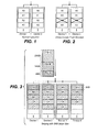
- FIG. 1 shows two devices, device 1 and device 2, which are connected in a mirroring arrangement (also referred to as RAID 1).
- Mirroring means that the same data that is stored in device 1, A0, A1, A2, A3, is also stored in device 2 so that there is a redundant copy of each unit of data in device 2.
- more than two devices may be connected in this way to provide more than two copies of the same data.
- maintaining a separate copy of the same data in two or more devices provides protection against failure of any individual device. Thus, if device 1 fails in FIG. 1 , all the data stored in device 1 can be recovered from device 2 instead.
- particular patterns of data storage may increase the chances of data becoming corrupted. This may occur because of the interaction between adjacent cells, with floating gates of cells affecting not only their underlying channels, but also affecting neighboring channels and thus affecting threshold voltages of neighboring cells. This is especially a problem for MLC memory systems in which small changes in a cell's threshold voltage may result in one or more bits stored in the cell being incorrectly read. The problem tends to become more severe as dimensions in memory arrays become smaller and interactions between cells become stronger.
- an MLC cell that is initially programmed to a low threshold voltage may later have its threshold voltage raised because neighboring cells are programmed to high threshold voltages (large charges on their floating gates).
- This may be considered a form of program disturb.
- Which specific data patterns cause program disturb, and the degree of disturb caused depends on the memory architecture.
- ECC Error Correction Coding
- the data is stored with some redundancy.
- the redundancy allows the data to be checked for errors, and up to some limited number of errors may be corrected.
- a high degree of redundancy is needed (a large number of extra bits) which is not an efficient use of memory space.
- the degree of redundancy used is based on expected error rates (e.g. based on a number of expected defective cells) and may not be sufficient to correct a high number of errors, such as caused by a particular data pattern.
- data pattern induced errors may occur together in the same portion of data in cells that are exposed to similar conditions, and ECC is generally limited to correcting only a limited number of bits in such a portion of data. Thus, ECC alone may not be sufficient to overcome data pattern induced errors in certain memory systems.
- FIG. 2 shows an example where device 1 and device 2 store identical copies of the same data.
- a portion of data A2 has a data pattern such that when A2 is stored and later read, the data that is read has a high number of errors because of interaction between cells. This may include interaction of cells within A2 and interaction with cells outside A2. In particular, cells in a row tend to be affected by cells in adjacent rows of the same block. In this case, the number of errors in data A2 is beyond the correcting capability of the ECC scheme being used and the data is considered to be uncorrectable by ECC.
- Data portion A2 may be any unit of data, such as a sector of 512 bytes (plus overhead), a page (unit of writing) or a block (minimum unit of erase).
- Data A2 is stored identically in both device 1 and device 2, so the same pattern occurs in each device. Therefore, copies of data A2 in both devices are affected and neither copy is recoverable. Thus, in this case, mirroring alone does not provide a sufficient level of reliability to enable all data to be recovered.
- FIG. 3 shows a first example of data striping between different devices (RAID 0). Data is received as three files, File A, File B and File C as shown. These files are then spread out across devices 1-4 as shown. In particular, File A is stored as A0 in device 1 and A1 in device 2. File B is stored as B0-B6, which are spread out across devices 1-4. And File C is stored as C0-C9, which are spread out across devices 1-4.
- a stripe of data in this example consists of one unit of data in each device, e.g. A0, A1, B0 and B1 together make up a stripe. Each stripe contains 2KBytes of data in this example.
- striping does not provide any redundancy, it can improve reliability because data is broken up and data patterns that might otherwise induce errors may be avoided. Striping data may improve performance because it facilitates programming with a high degree of parallelism across multiple devices.
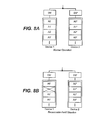
- FIG. 5A shows an example of a memory system using a combination of mirroring and striping.
- Data is striped between device 1 and device 2, and the data in devices 1 and 2 is mirrored in devices 3 and 4.
- This hybrid arrangement applying aspects of RAID 0 and RAID 1 may be referred to as RAID 0+1.
- FIG. 5B this arrangement still suffers problems when certain patterns occur in the stored data. In particular, if storage of data A2 in device 1 causes an uncorrectable number of errors due to the data pattern, then the copy of data A2 stored in device 3 also contains an uncorrectable number of errors. Similarly, the two copies of data A7, in device 2 and device 4, are both uncorrectable, so there is no recoverable copy of either A2 or A7.
- FIG. 6A shows an alternative combination of RAID 0 and RAID 1, which may be referred to as RAID 10.
- RAID 10 data in device 1 is mirrored in device 2.
- the same data that is stored in devices 1 and 2 is striped across device 3 and device 4.
- FIG. 6B where one copy of data A2 is uncorrectable because of its data pattern, then the other copies of data A2 in other devices are also uncorrectable.
- One approach to data patterns that may cause data to be uncorrectable when it is read is to scramble data before storage. Scrambling subjects data to some transformation so that the transformed data has a different pattern to untransformed data. In particular, such scrambling may introduce some randomization into a repeated pattern in the data.
- a simple example of a transformation is to invert (or flip) all bits, i.e. change all zeros to ones and change all ones to zeros.
- Other transformations involve performing exclusive OR (XOR) operations on data to be stored and some series of bits. Unlike ECC, scrambling does not add redundant bits, so the scrambled data includes the same number of bits as the original data. In some cases, a transformation may compress data, reducing the number of bits to be stored.
- FIG. 7A shows an example where a data scrambler unit, or Data Scrambler (DS), is connected to devices 1-4 so that all data to be stored in devices 1-4 is scrambled before storage. Scrambling is indicated in FIG. 7A by an apostrophe so that A0 is transformed to become A0' etc.
- FIG. 7A shows a RAID 10 arrangement as in FIG. 6A , with data mirrored between device 1 and device 2, and the same data striped across device 3 and device 4. While scrambling data may result in transformed data that has a pattern that does not cause disturbs, in some cases the transformed data will have a pattern that causes errors when reading. In some cases, data that without scrambling would not cause errors is transformed into a pattern that does cause errors.
- FIG. 7A shows an example where a data scrambler unit, or Data Scrambler (DS), is connected to devices 1-4 so that all data to be stored in devices 1-4 is scrambled before storage. Scrambling is indicated in FIG. 7A by an apos
- FIG. 8A shows a data storage system.
- the memory system receives a sequence of units of data A0, A1, A2, A3... which are transformed by the first data scrambler DS' according to a first transformation.
- the data transformed by DS' (A0', A1', A2', A3'...) is stored in device 1.
- Data A0, A1, A2, A3... are also transformed by a second data scrambler DS* (into A0*, A1*, A2*, A3*...) and stored.
- data A0 is transformed into A0' for storage in device 1 and data A0 is transformed into A0* for storage in device 2.
- Data A0' has a different pattern to data A0*.
- the threshold voltages of cells of device 1 storing data A0' may not be the same as corresponding cells in device 2 that store data A0*.
- different copies undergo different transformations before storage so that the same data pattern is not reproduced.
- scrambled data may have a pattern that causes the stored data to be uncorrectable.
- FIG. 8B shows transformed data A1' being uncorrectable due to its data pattern when stored.
- transformed data A1* has a different data pattern when stored, so transformed data A1* is not uncorrectable.
- a copy of original (untransformed) data A1 can be obtained from data A1*.
- FIG. 8B provides protection against device failure (i.e. if either device 1 or device 2 fails) and data pattern induced errors. While this method is similar to mirroring in that the data is stored in two independent devices, the two devices hold different data pattern as a result of scrambling. Thus, the data in device 2 does not mirror the data in device 1 and this is not true mirroring.
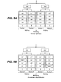
- FIG. 9A shows another example using RAID 0+1 with two different scrambler units DS', DS* performing two different transformations of data.
- Data scrambler DS' serves device 1 and device 2
- data scrambler DS* serves device 3 and device 4.
- All data stored in device 1 and device 2 is subject to a first transformation, while the same data is subject to a second transformation before storage in device 3 and device 4.
- Data is striped between device 1 and device 2, and data is also striped between device 3 and device 4.
- banks of more than two devices may share a data scrambler and have data striped in this manner.
- FIG. 9B shows data pattern induced errors occurring in transformed data A2' and in transformed data A7*.
- Original data A2 may be recovered by reading A2* and transforming it (reversing the transformation that created A2*). Because A2* has a different data pattern than A2' when stored, it is unlikely that both patterns induce errors. Similarly, even though A7* is unrecoverable, original data A7 can be recreated from A7'.
- the striping used in this example may allow a greater degree of parallelism during programming, which improves performance. While a different data scrambler unit may be provided for each device (i.e. separate data scrambler for devices 1, 2, 3, and 4), it is generally sufficient to provide one data scrambler for a group of devices that store striped data because such devices generally do not contain more than one copy of any particular portion of data.
- FIG. 10A shows an alternative memory system that has a RAID 10 configuration.
- Data received by the memory system is subject to a first transformation by data scrambler DS' before it is stored in device 1.
- the received data is also subject to a second transformation by data scrambler DS* before being stored in device 2.
- the received data is also subject to a third transformation by data scrambler DS" before being stored in device 3 and device 4.
- the transformed data is striped across device 3 and device 4.
- FIG. 10B shows data A2' and data A3" being unrecoverable because of data pattern induced errors.
- there are two other versions (A2*, A2", A3' and A3*) from which the original data can be recovered.
- FIG. 10C shows how portions of data A2' and A3" of FIG. 10B that are uncorrectable by ECC when read may be replaced by data generated from another device.
- A2' in device 1 is found to be uncorrectable by ECC
- original data A2 is recovered from data A2* stored in device 2.
- the original data A2 is also subject to yet another transformation to provide data A2**. This transformation is performed by modifying the transformation performed by data scrambler DS' to be different to the earlier transformation. After this replacement, there are three devices from which original data A2 can be recovered.
- data A3" in device 4 is uncorrectable by ECC, but original data A3 is recovered from data A3* in device 2.
- Original data A3 is then transformed to provide data A3**, which replaces uncorrectable data A3".
- the transformation of data A3 to A3** is performed by data scrambler DS", which is modified to perform a different transformation than was performed for previously stored data.
- data A2** and A3** are the result of a similar transformation.
- different transformations may be used in different devices when performing replacement.
- transformed data may be the product of an XOR operation on the original data and a key.
- the key may be changed periodically (e.g. changed for each sector, each page, each block or some other pattern).
- a limited number of keys are used, so that there is a repetitive pattern of key usage.
- only a fraction of the total number of keys may be used in any one device resulting in the key pattern repeating sooner than expected.
- FIG. 11A shows device 1 in which 32 keys (key 0 to key 31) are used to scramble data within a memory system having four devices (device 1 - device 4), the key changing from page to page.
- the pattern of key use repeats after 32 pages.
- this scheme is applied in a memory system using striping as shown in FIG. 11B , then the key repeats much sooner. In this case, after just 8 pages. It is generally undesirable for the pattern to repeat so soon because the risk of memory cells interacting is increased if the keys repeat sooner.
- FIG. 12A shows another example where a single data scrambler DS uses a limited number of keys to scramble data before the data is striped across devices 1-4.
- the keys used in each device are limited to a particular subset of keys, and the keys repeat within a device sooner as a result.
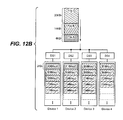
- FIG. 12B shows an alternative configuration where a different data scrambler is used for each device, with each data scrambler using a full set of keys so that all keys are used in each device. This increases the interval between reuse of the same key and so lowers the chances of memory cell states aligning in a manner that would result in data corruption. Thus, even where no redundancy is provided, using different scrambling for each device may be advantageous.
- FIG. 12B shows the same pattern of key use by each data scrambler.
- different data scramblers may use keys in different orders. For example, each data scrambler may start with a different key (e.g.
- data scrambler DS1 may start with key 0, data scrambler DS2 may start with key 8, data scrambler DS3 may start with key 16, and DS4 may start with key 24).
- Each scrambler may have an initial key, or seed, from which subsequent keys are derived.
- One way to ensure different transformations for data in different devices is to initialize their respective data scramblers using different seeds.
- data scramblers may be controlled so that different keys are used by each data scrambler when scrambling the same data.
- FIG. 13 shows an example of maintaining parity data in a dedicated device (RAID 4).
- parity data is stored exclusively in device 4.
- Parity data in device 4 is derived from data stored in devices 1-3. Parity data may be derived before or after data is scrambled. Parity information adds an extra level of protection against failure by allowing data in one device to be reconstructed from data in other devices including parity data.
- using parity data increases redundancy but also incurs a performance penalty because of the time to perform parity operations whenever data is written or read.
- Each device has a dedicated data scrambler, so that data scrambling keys are not frequently repeated within a device.
- FIG. 14 shows an example where parity data is distributed across all devices (RAID 5).
- each stripe includes parity data derived from the other data in the stripe.
- Parity0 is derived from A0, A1 and B0.
- Parity1 is derived from B1, B2 and B3. This example also shows dedicated data scramblers for each device.
- a dedicated data scrambler unit attached to an individual device. This may be achieved through hardware by having a dedicated circuit (e.g. a peripheral circuit on a memory die).
- data scrambling may be achieved by firmware in a controller so that the same hardware is used for different circuits, but the firmware ensures that different transformations are performed according to the destination device.
- Other hardware may also provide different scrambling to more than one device at a time. Thus, different scrambling schemes may be achieved without necessarily requiring different hardware for each device.
- the schemes described above may be combined with, or used to replace, other schemes that provide high reliability.
- the schemes are generally combined with an ECC scheme that provides protection against failure due to a small number of errors in a portion of data.
- the schemes described above are performed within a memory system (e.g. a removable memory card or USB flash drive) and may not be visible to a host.
- the degree of protection, or a particular protection scheme may be selected by a user, through the host, or otherwise.
- the host system may have its own protection scheme that is in addition to any protection scheme in the memory system.
Landscapes
- Engineering & Computer Science (AREA)
- Theoretical Computer Science (AREA)
- Quality & Reliability (AREA)
- Physics & Mathematics (AREA)
- General Engineering & Computer Science (AREA)
- General Physics & Mathematics (AREA)
- Techniques For Improving Reliability Of Storages (AREA)
- Storage Device Security (AREA)
- Error Detection And Correction (AREA)
Claims (15)
- Procédé de stockage sécurisé de données dans une matrice de mémoire non volatile, comprenant les étapes ci-dessous consistant à :transformer une partie de données (A0, A1, A2, A3, ...) selon une première transformation en vue d'obtenir des premières données transformées (A0', A1', A2', A3', ...) ;stocker les premières données transformées dans une première partie de la matrice de mémoire ;transformer la partie de données (A0, A1, A2, A3, ...) selon une deuxième transformation en vue d'obtenir des deuxièmes données transformées (A0*, A1*, A2*, A3*, ...) ;stocker les deuxièmes données transformées dans une deuxième partie de la matrice de mémoire tandis que les premières données transformées sont stockées dans la première partie de la matrice de mémoire, en vue de fournir un stockage redondant de la partie de données ;caractérisé par les étapes ci-dessous consistant à :subséquemment, en réponse à une tentative de lecture des premières données transformées à partir de la première partie de la matrice de mémoire, et à une détermination selon laquelle les premières données transformées (A2') ne peuvent pas être corrigées par un code de correction d'erreur, lire les deuxièmes données transformées (A2*) à partir de la deuxième partie de la matrice de mémoire ; etutiliser les deuxièmes données transformées (A2*) pour récupérer la partie de données (A2) et transformer subséquemment la partie de données selon une troisième transformation en vue d'obtenir des troisièmes données transformées (A2**), stocker les troisièmes données transformées dans une troisième partie de la matrice de mémoire, et effacer les premières données transformées stockées (A2') ;dans lequel les première, deuxième et troisième transformations sont différentes.
- Procédé selon la revendication 1, dans lequel la première transformation embrouille des données sur la base d'une première semence, et la deuxième transformation embrouille des données sur la base d'une seconde semence.
- Procédé selon la revendication 1 ou 2, dans lequel la transformation de la partie de données selon la première transformation est mise en oeuvre en parallèle à la transformation de la partie de données selon la deuxième transformation.
- Procédé selon la revendication 1, 2 ou 3, dans lequel les opérations de transformation et de stockage sont répétées pour de multiples parties de données, dans lequel les transformations incluent l'embrouillage de parties de données sur la base de clés qui changent de page en page d'une même partie de la matrice de mémoire, ou de la première partie de la matrice de mémoire à la deuxième partie de la matrice de mémoire.
- Procédé selon l'une quelconque des revendications précédentes, dans lequel la première partie de la matrice de mémoire correspond à un premier bloc et la deuxième partie de la matrice de mémoire correspond à un second bloc.
- Procédé selon l'une quelconque des revendications 1 à 4, dans lequel la première partie de la matrice de mémoire correspond à un premier plan et la deuxième partie de la matrice de mémoire correspond à un second plan.
- Procédé selon l'une quelconque des revendications 1 à 4, dans lequel la première partie de la matrice de mémoire correspond à une première puce et la deuxième partie de la matrice de mémoire correspond à une seconde puce.
- Système de mémoire non volatile comprenant :une matrice de mémoire ;un contrôleur de mémoire configuré de manière à mettre en oeuvre les opérations ci-dessous consistant à :transformer une partie de données (A0, A1, A2, A3, ...) selon une première transformation en vue d'obtenir des premières données transformées (A0', A1', A2', A3', ...) ;stocker les premières données transformées dans une première partie de la matrice de mémoire ;transformer la partie de données (A0, A1, A2, A3, ...) selon une deuxième transformation en vue d'obtenir des deuxièmes données transformées (A0*, A1*, A2*, A3*, ...) ;stocker les deuxièmes données transformées dans une deuxième partie de la matrice de mémoire tandis que les premières données transformées sont stockées dans la première partie de la matrice de mémoire, en vue de fournir un stockage redondant de la partie de données ;caractérisé en ce que :le contrôleur de mémoire est en outre configuré de manière à mettre en oeuvre les opérations ci-dessous consistant à :subséquemment, en réponse à une tentative de lecture des premières données transformées (A2') à partir de la première partie de la matrice de mémoire, et à une détermination selon laquelle les premières données transformées (A2') ne peuvent pas être corrigées par un code de correction d'erreur, lire les deuxièmes données transformées (A2*) à partir de la deuxième partie de la matrice de mémoire ; etutiliser les deuxièmes données transformées (A2*) pour récupérer la partie de données (A2) et transformer subséquemment la partie de données (A2) selon une troisième transformation en vue d'obtenir des troisièmes données transformées (A2**), stocker les troisièmes données transformées dans une troisième partie de la matrice de mémoire, et effacer les premières données transformées stockées (A2') ;dans lequel les première, deuxième et troisième transformations sont différentes.
- Système de mémoire non volatile selon la revendication 8, dans lequel le contrôleur de mémoire comprend en outre une première unité d'embrouilleur (DS') qui contient un premier circuit OU exclusif (OUX) destiné à mettre en oeuvre des opérations OUX en utilisant un premier nombre, et une seconde unité d'embrouilleur (DS*) qui contient un second circuit OUX destiné à mettre en oeuvre des opérations OUX en utilisant un second nombre.
- Système de mémoire non volatile selon la revendication 8 ou 9, dans lequel la première partie de matrice de mémoire correspond à un premier bloc et la deuxième partie de matrice de mémoire correspond à un second bloc.
- Système de mémoire non volatile selon la revendication 8 ou 9, dans lequel la première partie de matrice de mémoire correspond à un premier plan et la deuxième partie de matrice de mémoire correspond à un second plan.
- Système de mémoire non volatile selon la revendication 8 ou 9, dans lequel la première partie de matrice de mémoire correspond à une première puce et la deuxième partie de matrice de mémoire correspond à une seconde puce.
- Système de mémoire non volatile selon l'une quelconque des revendications 8 à 12, dans lequel le système de mémoire est situé dans une carte mémoire amovible.
- Système de mémoire non volatile selon la revendication 9, dans lequel la première unité d'embrouilleur et la seconde unité d'embrouilleur embrouillent les mêmes données en parallèle.
- Système de mémoire non volatile selon l'une quelconque des revendications 8 à 14, dans lequel les première et deuxième transformations sont des transformations réversibles.
Applications Claiming Priority (2)
| Application Number | Priority Date | Filing Date | Title |
|---|---|---|---|
| US11/861,146 US7873803B2 (en) | 2007-09-25 | 2007-09-25 | Nonvolatile memory with self recovery |
| PCT/US2008/077267 WO2009042554A1 (fr) | 2007-09-25 | 2008-09-22 | Mémoire non volatile avec auto-récupération |
Publications (2)
| Publication Number | Publication Date |
|---|---|
| EP2193523A1 EP2193523A1 (fr) | 2010-06-09 |
| EP2193523B1 true EP2193523B1 (fr) | 2015-02-18 |
Family
ID=40282261
Family Applications (1)
| Application Number | Title | Priority Date | Filing Date |
|---|---|---|---|
| EP08833414.9A Not-in-force EP2193523B1 (fr) | 2007-09-25 | 2008-09-22 | Mémoire non volatile avec auto-récupération |
Country Status (7)
| Country | Link |
|---|---|
| US (1) | US7873803B2 (fr) |
| EP (1) | EP2193523B1 (fr) |
| JP (1) | JP5341896B2 (fr) |
| KR (1) | KR20100075891A (fr) |
| CN (1) | CN101809673B (fr) |
| TW (1) | TWI391931B (fr) |
| WO (1) | WO2009042554A1 (fr) |
Families Citing this family (84)
| Publication number | Priority date | Publication date | Assignee | Title |
|---|---|---|---|---|
| CA2587055A1 (fr) * | 2004-11-05 | 2006-05-18 | Commvault Systems, Inc. | Procede et systeme pour mettre en commun des dispositifs de stockage |
| US8489817B2 (en) | 2007-12-06 | 2013-07-16 | Fusion-Io, Inc. | Apparatus, system, and method for caching data |
| US8935302B2 (en) | 2006-12-06 | 2015-01-13 | Intelligent Intellectual Property Holdings 2 Llc | Apparatus, system, and method for data block usage information synchronization for a non-volatile storage volume |
| US8706968B2 (en) | 2007-12-06 | 2014-04-22 | Fusion-Io, Inc. | Apparatus, system, and method for redundant write caching |
| US9734086B2 (en) | 2006-12-06 | 2017-08-15 | Sandisk Technologies Llc | Apparatus, system, and method for a device shared between multiple independent hosts |
| US9495241B2 (en) | 2006-12-06 | 2016-11-15 | Longitude Enterprise Flash S.A.R.L. | Systems and methods for adaptive data storage |
| US8443134B2 (en) | 2006-12-06 | 2013-05-14 | Fusion-Io, Inc. | Apparatus, system, and method for graceful cache device degradation |
| US9116823B2 (en) | 2006-12-06 | 2015-08-25 | Intelligent Intellectual Property Holdings 2 Llc | Systems and methods for adaptive error-correction coding |
| US9104599B2 (en) | 2007-12-06 | 2015-08-11 | Intelligent Intellectual Property Holdings 2 Llc | Apparatus, system, and method for destaging cached data |
| US7836226B2 (en) | 2007-12-06 | 2010-11-16 | Fusion-Io, Inc. | Apparatus, system, and method for coordinating storage requests in a multi-processor/multi-thread environment |
| US8316277B2 (en) | 2007-12-06 | 2012-11-20 | Fusion-Io, Inc. | Apparatus, system, and method for ensuring data validity in a data storage process |
| US9519540B2 (en) | 2007-12-06 | 2016-12-13 | Sandisk Technologies Llc | Apparatus, system, and method for destaging cached data |
| US8799681B1 (en) * | 2007-12-27 | 2014-08-05 | Emc Corporation | Redundant array of encrypting disks |
| US8588425B1 (en) | 2007-12-27 | 2013-11-19 | Emc Corporation | Encryption key recovery in the event of storage management failure |
| US8301912B2 (en) | 2007-12-31 | 2012-10-30 | Sandisk Technologies Inc. | System, method and memory device providing data scrambling compatible with on-chip copy operation |
| US9830278B1 (en) | 2008-03-06 | 2017-11-28 | EMC IP Holding Company LLC | Tracking replica data using key management |
| US8059455B2 (en) * | 2008-05-09 | 2011-11-15 | Sandisk Il Ltd. | Partial scrambling to reduce correlation |
| US8533559B2 (en) * | 2008-05-12 | 2013-09-10 | Panasonic Corporation | Semiconductor recording device with error recovery |
| JP2009294869A (ja) * | 2008-06-04 | 2009-12-17 | Toshiba Corp | メモリシステム |
| US8843691B2 (en) * | 2008-06-25 | 2014-09-23 | Stec, Inc. | Prioritized erasure of data blocks in a flash storage device |
| KR20100124087A (ko) * | 2009-05-18 | 2010-11-26 | 삼성전자주식회사 | 메모리 컨트롤러, 그것을 포함하는 메모리 시스템 그리고 그것의 동작 방법 |
| TW201103033A (en) * | 2009-07-02 | 2011-01-16 | Silicon Motion Inc | Data accessing method and data accessing system utilizing the method |
| KR101717644B1 (ko) * | 2009-09-08 | 2017-03-27 | 샌디스크 테크놀로지스 엘엘씨 | 고체-상태 저장 디바이스 상에서 데이터를 캐싱하는 장치, 시스템, 및 방법 |
| WO2011031903A2 (fr) | 2009-09-09 | 2011-03-17 | Fusion-Io, Inc. | Appareil, système, et procédé d'attribution de stockage |
| US9122579B2 (en) | 2010-01-06 | 2015-09-01 | Intelligent Intellectual Property Holdings 2 Llc | Apparatus, system, and method for a storage layer |
| TWI497293B (zh) | 2009-12-17 | 2015-08-21 | Ibm | 固態儲存裝置內之資料管理 |
| JP5066199B2 (ja) | 2010-02-12 | 2012-11-07 | 株式会社東芝 | 半導体記憶装置 |
| JP4901968B2 (ja) * | 2010-03-01 | 2012-03-21 | 株式会社東芝 | 半導体記憶装置 |
| JP5017407B2 (ja) | 2010-03-24 | 2012-09-05 | 株式会社東芝 | 半導体記憶装置 |
| US8417877B2 (en) * | 2010-08-31 | 2013-04-09 | Micron Technology, Inc | Stripe-based non-volatile multilevel memory operation |
| US20120239860A1 (en) | 2010-12-17 | 2012-09-20 | Fusion-Io, Inc. | Apparatus, system, and method for persistent data management on a non-volatile storage media |
| JP2012137885A (ja) * | 2010-12-24 | 2012-07-19 | Toshiba Corp | データ記憶装置、メモリ制御装置及びメモリ制御方法 |
| JP5367686B2 (ja) | 2010-12-24 | 2013-12-11 | 株式会社東芝 | データ記憶装置、メモリ制御装置及びメモリ制御方法 |
| US8966184B2 (en) | 2011-01-31 | 2015-02-24 | Intelligent Intellectual Property Holdings 2, LLC. | Apparatus, system, and method for managing eviction of data |
| US9003104B2 (en) | 2011-02-15 | 2015-04-07 | Intelligent Intellectual Property Holdings 2 Llc | Systems and methods for a file-level cache |
| US9201677B2 (en) | 2011-05-23 | 2015-12-01 | Intelligent Intellectual Property Holdings 2 Llc | Managing data input/output operations |
| US8874823B2 (en) | 2011-02-15 | 2014-10-28 | Intellectual Property Holdings 2 Llc | Systems and methods for managing data input/output operations |
| WO2012116369A2 (fr) | 2011-02-25 | 2012-08-30 | Fusion-Io, Inc. | Appareil, système et procédé de gestion du contenu d'une antémémoire |
| US9563555B2 (en) | 2011-03-18 | 2017-02-07 | Sandisk Technologies Llc | Systems and methods for storage allocation |
| US8966191B2 (en) | 2011-03-18 | 2015-02-24 | Fusion-Io, Inc. | Logical interface for contextual storage |
| KR101826137B1 (ko) | 2011-03-24 | 2018-03-22 | 삼성전자주식회사 | 메모리 컨트롤러, 이를 포함하는 장치들, 및 이의 동작 방법 |
| KR101818445B1 (ko) | 2011-07-08 | 2018-01-16 | 삼성전자주식회사 | 메모리 컨트롤러, 이의 동작 방법, 및 상기 메모리 컨트롤러를 포함하는 전자 장치들 |
| JP5644707B2 (ja) * | 2011-07-20 | 2014-12-24 | 株式会社デンソー | 電子制御装置及び制御システム |
| US9417821B2 (en) | 2011-09-30 | 2016-08-16 | Intel Corporation | Presentation of direct accessed storage under a logical drive model |
| US9274937B2 (en) | 2011-12-22 | 2016-03-01 | Longitude Enterprise Flash S.A.R.L. | Systems, methods, and interfaces for vector input/output operations |
| US10102117B2 (en) | 2012-01-12 | 2018-10-16 | Sandisk Technologies Llc | Systems and methods for cache and storage device coordination |
| US9251052B2 (en) | 2012-01-12 | 2016-02-02 | Intelligent Intellectual Property Holdings 2 Llc | Systems and methods for profiling a non-volatile cache having a logical-to-physical translation layer |
| US9767032B2 (en) | 2012-01-12 | 2017-09-19 | Sandisk Technologies Llc | Systems and methods for cache endurance |
| US8782344B2 (en) | 2012-01-12 | 2014-07-15 | Fusion-Io, Inc. | Systems and methods for managing cache admission |
| US9251086B2 (en) | 2012-01-24 | 2016-02-02 | SanDisk Technologies, Inc. | Apparatus, system, and method for managing a cache |
| US9116812B2 (en) | 2012-01-27 | 2015-08-25 | Intelligent Intellectual Property Holdings 2 Llc | Systems and methods for a de-duplication cache |
| US10019353B2 (en) | 2012-03-02 | 2018-07-10 | Longitude Enterprise Flash S.A.R.L. | Systems and methods for referencing data on a storage medium |
| US9459955B2 (en) | 2012-05-24 | 2016-10-04 | Sandisk Technologies Llc | System and method to scramble data based on a scramble key |
| US9612966B2 (en) | 2012-07-03 | 2017-04-04 | Sandisk Technologies Llc | Systems, methods and apparatus for a virtual machine cache |
| US10339056B2 (en) | 2012-07-03 | 2019-07-02 | Sandisk Technologies Llc | Systems, methods and apparatus for cache transfers |
| US10346095B2 (en) | 2012-08-31 | 2019-07-09 | Sandisk Technologies, Llc | Systems, methods, and interfaces for adaptive cache persistence |
| US10318495B2 (en) | 2012-09-24 | 2019-06-11 | Sandisk Technologies Llc | Snapshots for a non-volatile device |
| US10509776B2 (en) | 2012-09-24 | 2019-12-17 | Sandisk Technologies Llc | Time sequence data management |
| FR3001818B1 (fr) * | 2013-02-05 | 2016-06-24 | Airbus Operations Sas | Dispositif de stockage redondant securise et procede de lecture ecriture securise sur un tel dispositif |
| CN104008069B (zh) * | 2013-02-22 | 2018-06-15 | 中兴通讯股份有限公司 | 一种数据保护方法、装置及设备 |
| US9842053B2 (en) | 2013-03-15 | 2017-12-12 | Sandisk Technologies Llc | Systems and methods for persistent cache logging |
| US10558561B2 (en) | 2013-04-16 | 2020-02-11 | Sandisk Technologies Llc | Systems and methods for storage metadata management |
| US10102144B2 (en) | 2013-04-16 | 2018-10-16 | Sandisk Technologies Llc | Systems, methods and interfaces for data virtualization |
| TWI502601B (zh) * | 2013-04-24 | 2015-10-01 | Ind Tech Res Inst | 混合式錯誤修復方法及其記憶體裝置 |
| US9842128B2 (en) | 2013-08-01 | 2017-12-12 | Sandisk Technologies Llc | Systems and methods for atomic storage operations |
| US10019320B2 (en) | 2013-10-18 | 2018-07-10 | Sandisk Technologies Llc | Systems and methods for distributed atomic storage operations |
| US10073630B2 (en) | 2013-11-08 | 2018-09-11 | Sandisk Technologies Llc | Systems and methods for log coordination |
| KR102133542B1 (ko) | 2013-12-03 | 2020-07-14 | 에스케이하이닉스 주식회사 | 랜더마이저 및 디랜더마이저를 포함하는 메모리 시스템 |
| US9747967B2 (en) | 2014-09-26 | 2017-08-29 | Intel Corporation | Magnetic field-assisted memory operation |
| US20160188890A1 (en) * | 2014-12-26 | 2016-06-30 | Intel Corporation | Security mode data protection |
| US9946607B2 (en) | 2015-03-04 | 2018-04-17 | Sandisk Technologies Llc | Systems and methods for storage error management |
| US9952784B2 (en) | 2015-03-11 | 2018-04-24 | Sandisk Technologies Llc | Multichip dual write |
| KR102319402B1 (ko) | 2015-06-30 | 2021-11-01 | 에스케이하이닉스 주식회사 | 복수의 채널들을 통해 반도체 메모리 장치들을 제어하는 메모리 시스템 |
| JP6178909B1 (ja) * | 2016-09-15 | 2017-08-09 | ウィンボンド エレクトロニクス コーポレーション | 不揮発性半導体記憶装置 |
| US20180095985A1 (en) * | 2016-09-30 | 2018-04-05 | Cubistolabs, Inc. | Physical Location Scrambler for Hashed Data De-Duplicating Content-Addressable Redundant Data Storage Clusters |
| US10394648B2 (en) * | 2016-11-07 | 2019-08-27 | Samsung Electronics Co., Ltd. | Method to deliver in-DRAM ECC information through DDR bus |
| CN108572887A (zh) * | 2017-03-14 | 2018-09-25 | 上海骐宏电驱动科技有限公司 | 数据检验校正方法 |
| US10755787B2 (en) | 2018-06-28 | 2020-08-25 | Apple Inc. | Efficient post programming verification in a nonvolatile memory |
| US10762967B2 (en) | 2018-06-28 | 2020-09-01 | Apple Inc. | Recovering from failure in programming a nonvolatile memory |
| US10936455B2 (en) | 2019-02-11 | 2021-03-02 | Apple Inc. | Recovery of data failing due to impairment whose severity depends on bit-significance value |
| US10915394B1 (en) | 2019-09-22 | 2021-02-09 | Apple Inc. | Schemes for protecting data in NVM device using small storage footprint |
| KR102923313B1 (ko) | 2020-03-03 | 2026-02-05 | 에스케이하이닉스 주식회사 | 메모리 컨트롤러 및 그것의 동작 방법 |
| US11250913B2 (en) | 2020-05-21 | 2022-02-15 | Western Digital Technologies, Inc. | Scrambling using different scrambling seeds for defect reduction and improved programming efficiency |
| US11550657B1 (en) | 2021-09-01 | 2023-01-10 | Apple Inc. | Efficient programming schemes in a nonvolatile memory |
Family Cites Families (22)
| Publication number | Priority date | Publication date | Assignee | Title |
|---|---|---|---|---|
| US4092732A (en) | 1977-05-31 | 1978-05-30 | International Business Machines Corporation | System for recovering data stored in failed memory unit |
| DD245068B1 (de) | 1985-12-23 | 1990-03-21 | Freiberg Brennstoffinst | Anordnung zur pruefung von schreib-lesespeichern |
| US4761785B1 (en) | 1986-06-12 | 1996-03-12 | Ibm | Parity spreading to enhance storage access |
| US4870643A (en) | 1987-11-06 | 1989-09-26 | Micropolis Corporation | Parallel drive array storage system |
| JPH0741642U (ja) * | 1993-12-28 | 1995-07-21 | 横河電機株式会社 | 二重化記憶装置 |
| JP3065481B2 (ja) | 1994-04-22 | 2000-07-17 | インターナショナル・ビジネス・マシーンズ・コーポレ−ション | ディスク・アレイ装置およびデータの格納方法 |
| EP0709782B1 (fr) | 1994-10-25 | 1999-03-03 | Hewlett-Packard Company | Système et méthode de détection d'erreurs pour mémoire reflétée entre contrÔleurs doublés de disque mémoire |
| DE19540915A1 (de) | 1994-11-10 | 1996-05-15 | Raymond Engineering | Redundante Anordnung von Festkörper-Speicherbausteinen |
| US6404647B1 (en) | 2000-08-24 | 2002-06-11 | Hewlett-Packard Co. | Solid-state mass memory storage device |
| US20020174295A1 (en) | 2001-01-29 | 2002-11-21 | Ulrich Thomas R. | Enhanced file system failure tolerance |
| DE10113319A1 (de) | 2001-03-20 | 2002-09-26 | Conti Temic Microelectronic | Verfahren zum Betrieb eines von einem Prozessor gesteuerten Systems |
| US6928590B2 (en) | 2001-12-14 | 2005-08-09 | Matrix Semiconductor, Inc. | Memory device and method for storing bits in non-adjacent storage locations in a memory array |
| US6941412B2 (en) | 2002-08-29 | 2005-09-06 | Sandisk Corporation | Symbol frequency leveling in a storage system |
| JP3748847B2 (ja) * | 2002-10-30 | 2006-02-22 | コナミ株式会社 | 格納装置、プログラム、ならびに、格納方法 |
| JP2004361986A (ja) * | 2003-04-08 | 2004-12-24 | Sharp Corp | スクランブル回路 |
| US7139864B2 (en) * | 2003-12-30 | 2006-11-21 | Sandisk Corporation | Non-volatile memory and method with block management system |
| US7093157B2 (en) | 2004-06-17 | 2006-08-15 | International Business Machines Corporation | Method and system for autonomic protection against data strip loss |
| JP4543317B2 (ja) * | 2004-12-07 | 2010-09-15 | 株式会社デンソー | 不揮発性メモリのデータ制御方法 |
| US20060143505A1 (en) | 2004-12-22 | 2006-06-29 | Dell Products L.P. | Method of providing data security between raid controller and disk drives |
| JP4667093B2 (ja) * | 2005-03-17 | 2011-04-06 | 富士通株式会社 | 二重化記憶装置及び二重化記憶装置の制御方法 |
| WO2007089369A2 (fr) * | 2005-12-27 | 2007-08-09 | Sandisk Corporation | Procede d'enregistrement de micrologiciel telechargeable sur supports de masse |
| US7546515B2 (en) | 2005-12-27 | 2009-06-09 | Sandisk Corporation | Method of storing downloadable firmware on bulk media |
-
2007
- 2007-09-25 US US11/861,146 patent/US7873803B2/en active Active
-
2008
- 2008-09-22 EP EP08833414.9A patent/EP2193523B1/fr not_active Not-in-force
- 2008-09-22 KR KR1020107007383A patent/KR20100075891A/ko not_active Withdrawn
- 2008-09-22 JP JP2010526051A patent/JP5341896B2/ja not_active Expired - Fee Related
- 2008-09-22 WO PCT/US2008/077267 patent/WO2009042554A1/fr not_active Ceased
- 2008-09-22 CN CN2008801083019A patent/CN101809673B/zh active Active
- 2008-09-24 TW TW097136681A patent/TWI391931B/zh not_active IP Right Cessation
Also Published As
| Publication number | Publication date |
|---|---|
| JP5341896B2 (ja) | 2013-11-13 |
| JP2010541049A (ja) | 2010-12-24 |
| CN101809673A (zh) | 2010-08-18 |
| TWI391931B (zh) | 2013-04-01 |
| EP2193523A1 (fr) | 2010-06-09 |
| TW200921676A (en) | 2009-05-16 |
| KR20100075891A (ko) | 2010-07-05 |
| WO2009042554A1 (fr) | 2009-04-02 |
| CN101809673B (zh) | 2013-07-03 |
| US20090083485A1 (en) | 2009-03-26 |
| US7873803B2 (en) | 2011-01-18 |
Similar Documents
| Publication | Publication Date | Title |
|---|---|---|
| EP2193523B1 (fr) | Mémoire non volatile avec auto-récupération | |
| US7953930B2 (en) | Device identifiers for nonvolatile memory modules | |
| US11531590B2 (en) | Method and system for host-assisted data recovery assurance for data center storage device architectures | |
| US10635585B2 (en) | On-chip copy with data folding in three-dimensional non-volatile memory array | |
| US8438455B2 (en) | Error correction in a solid state disk | |
| EP1883884B1 (fr) | Procede de gestion de memoire flash resistant a la degradation des donnees par perte d'alimentation | |
| US8132045B2 (en) | Program failure handling in nonvolatile memory | |
| US8473814B2 (en) | MLC self-RAID flash data protection scheme | |
| CN107678695B (zh) | 基于可用存储器空间选择冗余存储配置 | |
| US9037902B2 (en) | Flash memory techniques for recovering from write interrupt resulting from voltage fault | |
| US20120324148A1 (en) | System and method of protecting metadata from nand flash failures | |
| US10133645B2 (en) | Data recovery in three dimensional non-volatile memory array after word line short | |
| US20160216910A1 (en) | Solving MLC NAND paired page program using reduced spatial redundancy | |
| US11029874B2 (en) | Rolling XOR protection in efficient pipeline | |
| CN113302699A (zh) | 存储器中的单调计数器 | |
| CN119025019A (zh) | 存储器装置的数据存取管理的方法、存储器装置的存储器控制器、存储器装置以及电子装置 | |
| TWI862437B (zh) | 用來進行預定通訊架構中的記憶體裝置的資料存取管理的方法、記憶體裝置的記憶體控制器、記憶體裝置以及電子裝置 | |
| CN121666619A (zh) | 用于操作存储器系统的设备、系统和方法 |
Legal Events
| Date | Code | Title | Description |
|---|---|---|---|
| PUAI | Public reference made under article 153(3) epc to a published international application that has entered the european phase |
Free format text: ORIGINAL CODE: 0009012 |
|
| 17P | Request for examination filed |
Effective date: 20100318 |
|
| AK | Designated contracting states |
Kind code of ref document: A1 Designated state(s): AT BE BG CH CY CZ DE DK EE ES FI FR GB GR HR HU IE IS IT LI LT LU LV MC MT NL NO PL PT RO SE SI SK TR |
|
| AX | Request for extension of the european patent |
Extension state: AL BA MK RS |
|
| DAX | Request for extension of the european patent (deleted) | ||
| RAP1 | Party data changed (applicant data changed or rights of an application transferred) |
Owner name: SANDISK TECHNOLOGIES INC. |
|
| 17Q | First examination report despatched |
Effective date: 20120814 |
|
| GRAP | Despatch of communication of intention to grant a patent |
Free format text: ORIGINAL CODE: EPIDOSNIGR1 |
|
| INTG | Intention to grant announced |
Effective date: 20140822 |
|
| GRAS | Grant fee paid |
Free format text: ORIGINAL CODE: EPIDOSNIGR3 |
|
| GRAA | (expected) grant |
Free format text: ORIGINAL CODE: 0009210 |
|
| AK | Designated contracting states |
Kind code of ref document: B1 Designated state(s): AT BE BG CH CY CZ DE DK EE ES FI FR GB GR HR HU IE IS IT LI LT LU LV MC MT NL NO PL PT RO SE SI SK TR |
|
| REG | Reference to a national code |
Ref country code: GB Ref legal event code: FG4D |
|
| REG | Reference to a national code |
Ref country code: CH Ref legal event code: EP |
|
| REG | Reference to a national code |
Ref country code: AT Ref legal event code: REF Ref document number: 710930 Country of ref document: AT Kind code of ref document: T Effective date: 20150315 |
|
| REG | Reference to a national code |
Ref country code: IE Ref legal event code: FG4D |
|
| REG | Reference to a national code |
Ref country code: DE Ref legal event code: R096 Ref document number: 602008036694 Country of ref document: DE Effective date: 20150402 |
|
| REG | Reference to a national code |
Ref country code: NL Ref legal event code: VDEP Effective date: 20150218 |
|
| REG | Reference to a national code |
Ref country code: AT Ref legal event code: MK05 Ref document number: 710930 Country of ref document: AT Kind code of ref document: T Effective date: 20150218 |
|
| REG | Reference to a national code |
Ref country code: LT Ref legal event code: MG4D |
|
| PG25 | Lapsed in a contracting state [announced via postgrant information from national office to epo] |
Ref country code: NO Free format text: LAPSE BECAUSE OF FAILURE TO SUBMIT A TRANSLATION OF THE DESCRIPTION OR TO PAY THE FEE WITHIN THE PRESCRIBED TIME-LIMIT Effective date: 20150518 Ref country code: SE Free format text: LAPSE BECAUSE OF FAILURE TO SUBMIT A TRANSLATION OF THE DESCRIPTION OR TO PAY THE FEE WITHIN THE PRESCRIBED TIME-LIMIT Effective date: 20150218 Ref country code: ES Free format text: LAPSE BECAUSE OF FAILURE TO SUBMIT A TRANSLATION OF THE DESCRIPTION OR TO PAY THE FEE WITHIN THE PRESCRIBED TIME-LIMIT Effective date: 20150218 Ref country code: HR Free format text: LAPSE BECAUSE OF FAILURE TO SUBMIT A TRANSLATION OF THE DESCRIPTION OR TO PAY THE FEE WITHIN THE PRESCRIBED TIME-LIMIT Effective date: 20150218 Ref country code: FI Free format text: LAPSE BECAUSE OF FAILURE TO SUBMIT A TRANSLATION OF THE DESCRIPTION OR TO PAY THE FEE WITHIN THE PRESCRIBED TIME-LIMIT Effective date: 20150218 Ref country code: LT Free format text: LAPSE BECAUSE OF FAILURE TO SUBMIT A TRANSLATION OF THE DESCRIPTION OR TO PAY THE FEE WITHIN THE PRESCRIBED TIME-LIMIT Effective date: 20150218 |
|
| PG25 | Lapsed in a contracting state [announced via postgrant information from national office to epo] |
Ref country code: AT Free format text: LAPSE BECAUSE OF FAILURE TO SUBMIT A TRANSLATION OF THE DESCRIPTION OR TO PAY THE FEE WITHIN THE PRESCRIBED TIME-LIMIT Effective date: 20150218 Ref country code: GR Free format text: LAPSE BECAUSE OF FAILURE TO SUBMIT A TRANSLATION OF THE DESCRIPTION OR TO PAY THE FEE WITHIN THE PRESCRIBED TIME-LIMIT Effective date: 20150519 Ref country code: NL Free format text: LAPSE BECAUSE OF FAILURE TO SUBMIT A TRANSLATION OF THE DESCRIPTION OR TO PAY THE FEE WITHIN THE PRESCRIBED TIME-LIMIT Effective date: 20150218 Ref country code: LV Free format text: LAPSE BECAUSE OF FAILURE TO SUBMIT A TRANSLATION OF THE DESCRIPTION OR TO PAY THE FEE WITHIN THE PRESCRIBED TIME-LIMIT Effective date: 20150218 Ref country code: IS Free format text: LAPSE BECAUSE OF FAILURE TO SUBMIT A TRANSLATION OF THE DESCRIPTION OR TO PAY THE FEE WITHIN THE PRESCRIBED TIME-LIMIT Effective date: 20150618 |
|
| PG25 | Lapsed in a contracting state [announced via postgrant information from national office to epo] |
Ref country code: DK Free format text: LAPSE BECAUSE OF FAILURE TO SUBMIT A TRANSLATION OF THE DESCRIPTION OR TO PAY THE FEE WITHIN THE PRESCRIBED TIME-LIMIT Effective date: 20150218 Ref country code: EE Free format text: LAPSE BECAUSE OF FAILURE TO SUBMIT A TRANSLATION OF THE DESCRIPTION OR TO PAY THE FEE WITHIN THE PRESCRIBED TIME-LIMIT Effective date: 20150218 Ref country code: RO Free format text: LAPSE BECAUSE OF FAILURE TO SUBMIT A TRANSLATION OF THE DESCRIPTION OR TO PAY THE FEE WITHIN THE PRESCRIBED TIME-LIMIT Effective date: 20150218 Ref country code: CZ Free format text: LAPSE BECAUSE OF FAILURE TO SUBMIT A TRANSLATION OF THE DESCRIPTION OR TO PAY THE FEE WITHIN THE PRESCRIBED TIME-LIMIT Effective date: 20150218 Ref country code: SK Free format text: LAPSE BECAUSE OF FAILURE TO SUBMIT A TRANSLATION OF THE DESCRIPTION OR TO PAY THE FEE WITHIN THE PRESCRIBED TIME-LIMIT Effective date: 20150218 |
|
| REG | Reference to a national code |
Ref country code: DE Ref legal event code: R097 Ref document number: 602008036694 Country of ref document: DE |
|
| PG25 | Lapsed in a contracting state [announced via postgrant information from national office to epo] |
Ref country code: PL Free format text: LAPSE BECAUSE OF FAILURE TO SUBMIT A TRANSLATION OF THE DESCRIPTION OR TO PAY THE FEE WITHIN THE PRESCRIBED TIME-LIMIT Effective date: 20150218 |
|
| PLBE | No opposition filed within time limit |
Free format text: ORIGINAL CODE: 0009261 |
|
| STAA | Information on the status of an ep patent application or granted ep patent |
Free format text: STATUS: NO OPPOSITION FILED WITHIN TIME LIMIT |
|
| PG25 | Lapsed in a contracting state [announced via postgrant information from national office to epo] |
Ref country code: IT Free format text: LAPSE BECAUSE OF FAILURE TO SUBMIT A TRANSLATION OF THE DESCRIPTION OR TO PAY THE FEE WITHIN THE PRESCRIBED TIME-LIMIT Effective date: 20150218 |
|
| 26N | No opposition filed |
Effective date: 20151119 |
|
| PG25 | Lapsed in a contracting state [announced via postgrant information from national office to epo] |
Ref country code: SI Free format text: LAPSE BECAUSE OF FAILURE TO SUBMIT A TRANSLATION OF THE DESCRIPTION OR TO PAY THE FEE WITHIN THE PRESCRIBED TIME-LIMIT Effective date: 20150218 |
|
| PG25 | Lapsed in a contracting state [announced via postgrant information from national office to epo] |
Ref country code: LU Free format text: LAPSE BECAUSE OF FAILURE TO SUBMIT A TRANSLATION OF THE DESCRIPTION OR TO PAY THE FEE WITHIN THE PRESCRIBED TIME-LIMIT Effective date: 20150922 Ref country code: MC Free format text: LAPSE BECAUSE OF FAILURE TO SUBMIT A TRANSLATION OF THE DESCRIPTION OR TO PAY THE FEE WITHIN THE PRESCRIBED TIME-LIMIT Effective date: 20150218 |
|
| REG | Reference to a national code |
Ref country code: CH Ref legal event code: PL |
|
| PG25 | Lapsed in a contracting state [announced via postgrant information from national office to epo] |
Ref country code: BE Free format text: LAPSE BECAUSE OF FAILURE TO SUBMIT A TRANSLATION OF THE DESCRIPTION OR TO PAY THE FEE WITHIN THE PRESCRIBED TIME-LIMIT Effective date: 20150218 |
|
| REG | Reference to a national code |
Ref country code: IE Ref legal event code: MM4A |
|
| REG | Reference to a national code |
Ref country code: FR Ref legal event code: ST Effective date: 20160531 |
|
| PG25 | Lapsed in a contracting state [announced via postgrant information from national office to epo] |
Ref country code: IE Free format text: LAPSE BECAUSE OF NON-PAYMENT OF DUE FEES Effective date: 20150922 Ref country code: CH Free format text: LAPSE BECAUSE OF NON-PAYMENT OF DUE FEES Effective date: 20150930 Ref country code: LI Free format text: LAPSE BECAUSE OF NON-PAYMENT OF DUE FEES Effective date: 20150930 |
|
| PG25 | Lapsed in a contracting state [announced via postgrant information from national office to epo] |
Ref country code: FR Free format text: LAPSE BECAUSE OF NON-PAYMENT OF DUE FEES Effective date: 20150930 |
|
| REG | Reference to a national code |
Ref country code: DE Ref legal event code: R082 Ref document number: 602008036694 Country of ref document: DE Representative=s name: MARKS & CLERK (LUXEMBOURG) LLP, LU Ref country code: DE Ref legal event code: R081 Ref document number: 602008036694 Country of ref document: DE Owner name: SANDISK TECHNOLOGIES LLC, PLANO, US Free format text: FORMER OWNER: SANDISK TECHNOLOGIES INC., PLANO, TEX., US |
|
| PG25 | Lapsed in a contracting state [announced via postgrant information from national office to epo] |
Ref country code: MT Free format text: LAPSE BECAUSE OF FAILURE TO SUBMIT A TRANSLATION OF THE DESCRIPTION OR TO PAY THE FEE WITHIN THE PRESCRIBED TIME-LIMIT Effective date: 20150218 |
|
| PG25 | Lapsed in a contracting state [announced via postgrant information from national office to epo] |
Ref country code: HU Free format text: LAPSE BECAUSE OF FAILURE TO SUBMIT A TRANSLATION OF THE DESCRIPTION OR TO PAY THE FEE WITHIN THE PRESCRIBED TIME-LIMIT; INVALID AB INITIO Effective date: 20080922 Ref country code: BG Free format text: LAPSE BECAUSE OF FAILURE TO SUBMIT A TRANSLATION OF THE DESCRIPTION OR TO PAY THE FEE WITHIN THE PRESCRIBED TIME-LIMIT Effective date: 20150218 |
|
| PG25 | Lapsed in a contracting state [announced via postgrant information from national office to epo] |
Ref country code: CY Free format text: LAPSE BECAUSE OF FAILURE TO SUBMIT A TRANSLATION OF THE DESCRIPTION OR TO PAY THE FEE WITHIN THE PRESCRIBED TIME-LIMIT Effective date: 20150218 |
|
| PG25 | Lapsed in a contracting state [announced via postgrant information from national office to epo] |
Ref country code: TR Free format text: LAPSE BECAUSE OF FAILURE TO SUBMIT A TRANSLATION OF THE DESCRIPTION OR TO PAY THE FEE WITHIN THE PRESCRIBED TIME-LIMIT Effective date: 20150218 |
|
| PG25 | Lapsed in a contracting state [announced via postgrant information from national office to epo] |
Ref country code: PT Free format text: LAPSE BECAUSE OF FAILURE TO SUBMIT A TRANSLATION OF THE DESCRIPTION OR TO PAY THE FEE WITHIN THE PRESCRIBED TIME-LIMIT Effective date: 20150218 |
|
| PGFP | Annual fee paid to national office [announced via postgrant information from national office to epo] |
Ref country code: GB Payment date: 20180919 Year of fee payment: 11 |
|
| PGFP | Annual fee paid to national office [announced via postgrant information from national office to epo] |
Ref country code: DE Payment date: 20190910 Year of fee payment: 12 |
|
| GBPC | Gb: european patent ceased through non-payment of renewal fee |
Effective date: 20190922 |
|
| PG25 | Lapsed in a contracting state [announced via postgrant information from national office to epo] |
Ref country code: GB Free format text: LAPSE BECAUSE OF NON-PAYMENT OF DUE FEES Effective date: 20190922 |
|
| REG | Reference to a national code |
Ref country code: DE Ref legal event code: R119 Ref document number: 602008036694 Country of ref document: DE |
|
| PG25 | Lapsed in a contracting state [announced via postgrant information from national office to epo] |
Ref country code: DE Free format text: LAPSE BECAUSE OF NON-PAYMENT OF DUE FEES Effective date: 20210401 |