EP2194425B1 - Anzeigeträger, Anzeigetafel mit dem Anzeigeträger und Anzeigevorrichtung mit der Anzeigetafel - Google Patents
Anzeigeträger, Anzeigetafel mit dem Anzeigeträger und Anzeigevorrichtung mit der Anzeigetafel Download PDFInfo
- Publication number
- EP2194425B1 EP2194425B1 EP09009612.4A EP09009612A EP2194425B1 EP 2194425 B1 EP2194425 B1 EP 2194425B1 EP 09009612 A EP09009612 A EP 09009612A EP 2194425 B1 EP2194425 B1 EP 2194425B1
- Authority
- EP
- European Patent Office
- Prior art keywords
- peripheral
- gate
- lines
- data
- area
- Prior art date
- Legal status (The legal status is an assumption and is not a legal conclusion. Google has not performed a legal analysis and makes no representation as to the accuracy of the status listed.)
- Active
Links
Images




Classifications
-
- G—PHYSICS
- G02—OPTICS
- G02F—OPTICAL DEVICES OR ARRANGEMENTS FOR THE CONTROL OF LIGHT BY MODIFICATION OF THE OPTICAL PROPERTIES OF THE MEDIA OF THE ELEMENTS INVOLVED THEREIN; NON-LINEAR OPTICS; FREQUENCY-CHANGING OF LIGHT; OPTICAL LOGIC ELEMENTS; OPTICAL ANALOGUE/DIGITAL CONVERTERS
- G02F1/00—Devices or arrangements for the control of the intensity, colour, phase, polarisation or direction of light arriving from an independent light source, e.g. switching, gating or modulating; Non-linear optics
- G02F1/01—Devices or arrangements for the control of the intensity, colour, phase, polarisation or direction of light arriving from an independent light source, e.g. switching, gating or modulating; Non-linear optics for the control of the intensity, phase, polarisation or colour
- G02F1/13—Devices or arrangements for the control of the intensity, colour, phase, polarisation or direction of light arriving from an independent light source, e.g. switching, gating or modulating; Non-linear optics for the control of the intensity, phase, polarisation or colour based on liquid crystals, e.g. single liquid crystal display cells
-
- H—ELECTRICITY
- H10—SEMICONDUCTOR DEVICES; ELECTRIC SOLID-STATE DEVICES NOT OTHERWISE PROVIDED FOR
- H10D—INORGANIC ELECTRIC SEMICONDUCTOR DEVICES
- H10D86/00—Integrated devices formed in or on insulating or conducting substrates, e.g. formed in silicon-on-insulator [SOI] substrates or on stainless steel or glass substrates
- H10D86/40—Integrated devices formed in or on insulating or conducting substrates, e.g. formed in silicon-on-insulator [SOI] substrates or on stainless steel or glass substrates characterised by multiple TFTs
- H10D86/60—Integrated devices formed in or on insulating or conducting substrates, e.g. formed in silicon-on-insulator [SOI] substrates or on stainless steel or glass substrates characterised by multiple TFTs wherein the TFTs are in active matrices
-
- G—PHYSICS
- G02—OPTICS
- G02F—OPTICAL DEVICES OR ARRANGEMENTS FOR THE CONTROL OF LIGHT BY MODIFICATION OF THE OPTICAL PROPERTIES OF THE MEDIA OF THE ELEMENTS INVOLVED THEREIN; NON-LINEAR OPTICS; FREQUENCY-CHANGING OF LIGHT; OPTICAL LOGIC ELEMENTS; OPTICAL ANALOGUE/DIGITAL CONVERTERS
- G02F1/00—Devices or arrangements for the control of the intensity, colour, phase, polarisation or direction of light arriving from an independent light source, e.g. switching, gating or modulating; Non-linear optics
- G02F1/01—Devices or arrangements for the control of the intensity, colour, phase, polarisation or direction of light arriving from an independent light source, e.g. switching, gating or modulating; Non-linear optics for the control of the intensity, phase, polarisation or colour
- G02F1/13—Devices or arrangements for the control of the intensity, colour, phase, polarisation or direction of light arriving from an independent light source, e.g. switching, gating or modulating; Non-linear optics for the control of the intensity, phase, polarisation or colour based on liquid crystals, e.g. single liquid crystal display cells
- G02F1/133—Constructional arrangements; Operation of liquid crystal cells; Circuit arrangements
-
- G—PHYSICS
- G02—OPTICS
- G02F—OPTICAL DEVICES OR ARRANGEMENTS FOR THE CONTROL OF LIGHT BY MODIFICATION OF THE OPTICAL PROPERTIES OF THE MEDIA OF THE ELEMENTS INVOLVED THEREIN; NON-LINEAR OPTICS; FREQUENCY-CHANGING OF LIGHT; OPTICAL LOGIC ELEMENTS; OPTICAL ANALOGUE/DIGITAL CONVERTERS
- G02F1/00—Devices or arrangements for the control of the intensity, colour, phase, polarisation or direction of light arriving from an independent light source, e.g. switching, gating or modulating; Non-linear optics
- G02F1/01—Devices or arrangements for the control of the intensity, colour, phase, polarisation or direction of light arriving from an independent light source, e.g. switching, gating or modulating; Non-linear optics for the control of the intensity, phase, polarisation or colour
- G02F1/13—Devices or arrangements for the control of the intensity, colour, phase, polarisation or direction of light arriving from an independent light source, e.g. switching, gating or modulating; Non-linear optics for the control of the intensity, phase, polarisation or colour based on liquid crystals, e.g. single liquid crystal display cells
- G02F1/133—Constructional arrangements; Operation of liquid crystal cells; Circuit arrangements
- G02F1/1333—Constructional arrangements; Manufacturing methods
- G02F1/1345—Conductors connecting electrodes to cell terminals
-
- G—PHYSICS
- G02—OPTICS
- G02F—OPTICAL DEVICES OR ARRANGEMENTS FOR THE CONTROL OF LIGHT BY MODIFICATION OF THE OPTICAL PROPERTIES OF THE MEDIA OF THE ELEMENTS INVOLVED THEREIN; NON-LINEAR OPTICS; FREQUENCY-CHANGING OF LIGHT; OPTICAL LOGIC ELEMENTS; OPTICAL ANALOGUE/DIGITAL CONVERTERS
- G02F1/00—Devices or arrangements for the control of the intensity, colour, phase, polarisation or direction of light arriving from an independent light source, e.g. switching, gating or modulating; Non-linear optics
- G02F1/01—Devices or arrangements for the control of the intensity, colour, phase, polarisation or direction of light arriving from an independent light source, e.g. switching, gating or modulating; Non-linear optics for the control of the intensity, phase, polarisation or colour
- G02F1/13—Devices or arrangements for the control of the intensity, colour, phase, polarisation or direction of light arriving from an independent light source, e.g. switching, gating or modulating; Non-linear optics for the control of the intensity, phase, polarisation or colour based on liquid crystals, e.g. single liquid crystal display cells
- G02F1/133—Constructional arrangements; Operation of liquid crystal cells; Circuit arrangements
- G02F1/136—Liquid crystal cells structurally associated with a semi-conducting layer or substrate, e.g. cells forming part of an integrated circuit
- G02F1/1362—Active matrix addressed cells
- G02F1/136286—Wiring, e.g. gate line, drain line
-
- G—PHYSICS
- G09—EDUCATION; CRYPTOGRAPHY; DISPLAY; ADVERTISING; SEALS
- G09G—ARRANGEMENTS OR CIRCUITS FOR CONTROL OF INDICATING DEVICES USING STATIC MEANS TO PRESENT VARIABLE INFORMATION
- G09G3/00—Control arrangements or circuits, of interest only in connection with visual indicators other than cathode-ray tubes
- G09G3/20—Control arrangements or circuits, of interest only in connection with visual indicators other than cathode-ray tubes for presentation of an assembly of a number of characters, e.g. a page, by composing the assembly by combination of individual elements arranged in a matrix no fixed position being assigned to or needed to be assigned to the individual characters or partial characters
-
- H—ELECTRICITY
- H10—SEMICONDUCTOR DEVICES; ELECTRIC SOLID-STATE DEVICES NOT OTHERWISE PROVIDED FOR
- H10D—INORGANIC ELECTRIC SEMICONDUCTOR DEVICES
- H10D86/00—Integrated devices formed in or on insulating or conducting substrates, e.g. formed in silicon-on-insulator [SOI] substrates or on stainless steel or glass substrates
- H10D86/40—Integrated devices formed in or on insulating or conducting substrates, e.g. formed in silicon-on-insulator [SOI] substrates or on stainless steel or glass substrates characterised by multiple TFTs
- H10D86/441—Interconnections, e.g. scanning lines
-
- G—PHYSICS
- G02—OPTICS
- G02F—OPTICAL DEVICES OR ARRANGEMENTS FOR THE CONTROL OF LIGHT BY MODIFICATION OF THE OPTICAL PROPERTIES OF THE MEDIA OF THE ELEMENTS INVOLVED THEREIN; NON-LINEAR OPTICS; FREQUENCY-CHANGING OF LIGHT; OPTICAL LOGIC ELEMENTS; OPTICAL ANALOGUE/DIGITAL CONVERTERS
- G02F2201/00—Constructional arrangements not provided for in groups G02F1/00 - G02F7/00
- G02F2201/56—Substrates having a particular shape, e.g. non-rectangular
-
- G—PHYSICS
- G09—EDUCATION; CRYPTOGRAPHY; DISPLAY; ADVERTISING; SEALS
- G09G—ARRANGEMENTS OR CIRCUITS FOR CONTROL OF INDICATING DEVICES USING STATIC MEANS TO PRESENT VARIABLE INFORMATION
- G09G2300/00—Aspects of the constitution of display devices
- G09G2300/04—Structural and physical details of display devices
- G09G2300/0421—Structural details of the set of electrodes
- G09G2300/0426—Layout of electrodes and connections
-
- G—PHYSICS
- G09—EDUCATION; CRYPTOGRAPHY; DISPLAY; ADVERTISING; SEALS
- G09G—ARRANGEMENTS OR CIRCUITS FOR CONTROL OF INDICATING DEVICES USING STATIC MEANS TO PRESENT VARIABLE INFORMATION
- G09G2310/00—Command of the display device
- G09G2310/02—Addressing, scanning or driving the display screen or processing steps related thereto
- G09G2310/0264—Details of driving circuits
- G09G2310/0281—Arrangement of scan or data electrode driver circuits at the periphery of a panel not inherent to a split matrix structure
Definitions
- the present invention relates to a display substrate, a display panel having the display substrate and a display device having the display panel. More particularly, the present invention relates to a display substrate used in a liquid crystal display (“LCD”) device, a display panel having the display substrate and a display device having the display panel.
- LCD liquid crystal display
- a liquid crystal display (“LCD”) device includes an LCD panel which displays an image using a light transmissivity of liquid crystal, and a backlight assembly which applies light to the LCD panel.
- LCD liquid crystal display
- the LCD panel includes a first substrate, a second substrate facing the first substrate and a liquid crystal layer interposed between the first substrate and the second substrate.
- the first substrate includes gate lines disposed along a first direction, data lines disposed along a second direction crossing, e.g., substantially perpendicular to, the first direction, thin-film transistors ("TFTs") electrically connected to the gate lines and the data lines, and pixel electrodes electrically connected to the TFTs.
- TFTs thin-film transistors
- the second substrate includes color filters corresponding to the pixel electrode and a common electrode disposed on a surface of the second substrate. An arrangement of the liquid crystal layer is altered by an electric field formed between the pixel electrode and the common electrode. Thus, light transmissivity through the liquid crystal layer is varied.
- the gate lines extend in the first direction to receive a gate signal from a gate driving part
- the data lines extend in the second direction crossing the first direction to receive a data signal from a data driving part
- the gate driving part is disposed at a first portion of the first substrate along the first direction to be electrically connected to the gate lines
- the data driving part is disposed at a second portion of the first substrate along the second direction to be electrically connected to the data lines.
- the LCD panel may have a rectangular shape when viewed from a top plan view perspective.
- US 5 270 693 is the document coming closest to the invention. It forms the preamble of claim 1.
- the said document discloses a matrix addressable display.
- the presently claimed subjected matter distinguishes from the teaching of the said document inter alia in the first gate driving part being electrically connected to the second data driving part by a first gate control line formed on the first peripheral area, the second gate driving part being electrically connected to the first data driving part by the second gate control line formed on the third peripheral area such that the first gate driving part is driven by the second data driving part and the second gate driving part is driven by the first data driving part.
- the entire routing circuitry can be carried out in a single plane on the substrate. Accordingly, it may be derived as an objective technical problem to provide a display device which provides for a reduction of the amount of electrical components, a reduced complexity in routing circuitry and lower costs of manufacture.
- Exemplary embodiments of the present invention provide a display substrate capable of having various shapes other than a rectangular shape.
- Exemplary embodiments of the present invention also provide a display panel having the display substrate.
- Exemplary embodiments of the present invention also provide a display device having the display panel.
- a display substrate includes a base substrate, a gate line portion, a data line portion and a pixel portion.
- the base substrate includes a first divided display area, a second divided display area, a third divided display area and a fourth divided display area that are sequentially disposed along a clockwise direction by dividing a display area into four areas for displaying an image; and a first peripheral area, a second peripheral area, a third peripheral area and a fourth peripheral area that are formed at peripheral portions of the first to fourth divided display areas, respectively.
- the gate line portion includes a plurality of first gate lines formed on the first and second divided display areas substantially parallel with the first direction, the first gate line being extended on the first peripheral area; and a plurality of second gate lines formed on the third and fourth dividing areas substantially parallel with the first direction, the second gate lines being extended on the third peripheral area.
- the data line portion includes a plurality of first data lines formed on the fourth and first divided display areas substantially parallel with the second direction, the first data line being extended on the fourth peripheral area; and a plurality of second data lines formed on the second and third divided display areas substantially parallel with the second direction, the second data lines being extended on the second peripheral area.
- the pixel portions are disposed in the display area in a matrix pattern. Each of the pixel portions is electrically connected to one of the first and second gate lines and one of the first and second data lines.
- the first gate lines may include a plurality of first gate main lines formed on the first and second divided display areas substantially parallel with the first direction, and a plurality of first gate peripheral lines formed on the first peripheral area to be connected to terminals of the first gate main lines, respectively.
- the second gate lines may include a plurality of second gate main lines formed on the third and fourth divided display areas substantially parallel with the first direction, and a plurality of gate peripheral lines formed on the third peripheral area to be connected to a terminal of the second gate main lines, respectively.
- the first data lines may include a plurality of first data main lines formed on the fourth and first divided display areas substantially parallel with the second direction, and a plurality of first data peripheral lines formed on the fourth peripheral area to be connected to a terminal of the first data main lines, respectively.
- the second data lines may include a plurality of second data main lines formed on the second and third divided display areas substantially parallel with the second direction, and a plurality of second data peripheral lines formed on the second peripheral area to be connected to a terminal of the second data main lines, respectively.
- the first gate peripheral lines may be extended in a longitudinal direction of the first peripheral area, and the second gate peripheral lines may be extended in a longitudinal direction of the third peripheral area.
- the first data peripheral lines may be extended in a longitudinal direction of the fourth peripheral area, and the second data peripheral lines may be extended in a longitudinal direction of the second peripheral area.
- all of the first and second gate peripheral lines and the first and second data peripheral lines may be extended in the same direction, which is identical to the clockwise direction or a counterclockwise direction.
- first gate peripheral lines may be extended in the clockwise direction, and another portion of the first gate peripheral lines may be extended in the counterclockwise direction.
- a portion of the second gate peripheral lines may be extended in the clockwise direction, and another portion of the second gate peripheral lines may be extended in the counterclockwise direction.
- a portion of the first data peripheral lines may be extended in the clockwise direction, and another portion of the first data peripheral lines may be extended in the counterclockwise direction.
- a portion of the second data peripheral lines may be extended in the clockwise direction, and another portion of the second data peripheral lines may be extended in the counterclockwise direction.
- the number of the clockwise first gate peripheral lines may be substantially equal to the number of the counterclockwise first gate peripheral lines.
- the number of the clockwise second gate peripheral lines may be substantially equal to the number of the counterclockwise second gate peripheral lines.
- the number of the clockwise first data peripheral lines may be substantially equal to the number of the counterclockwise first data peripheral lines.
- the number of the clockwise second data peripheral lines may be substantially equal to the number of the counterclockwise second data peripheral lines.
- first gate peripheral lines and the second gate peripheral lines may be extended in a direction identical to the clockwise direction or the counterclockwise direction
- first data peripheral lines and the second data peripheral lines may be extended in a direction identical to the clockwise direction or the counterclockwise direction.
- the first gate peripheral lines and the first data peripheral lines may be extended in directions opposite to each other
- the second gate peripheral lines and the second data peripheral lines may be extended in directions opposite to each other.
- the display area may have a circular or polygonal shape.
- the display area may have a symmetrical shape with respect to the first and second directions.
- all of the first to fourth peripheral areas may be extended along the peripheral portions of the display area.
- the base substrate may further include a first protruding area extended outwardly from the first peripheral area; a second protruding area extended outwardly from the second peripheral area; a third protruding area extended outwardly from the third peripheral area; and a fourth protruding area extended outwardly from the fourth peripheral area.
- the first gate lines may be extended from the first peripheral area to the first protruding area
- the second gate lines may be extended from the third peripheral area to the third protruding area
- the first data lines may be extended from the fourth peripheral area to the fourth protruding area
- the second data lines may be extended from the second peripheral area to the second protruding area.
- the display substrate may further include a first gate driving part formed on the first protruding area to be electrically connected to the first gate lines, the first gate driving part applying each of first gate signals to the first gate lines; and a second gate driving part formed on the third protruding area to be electrically connected to the second gate lines, the second gate driving part applying each of second gate signals to the second gate lines.
- each of the pixel portions may include a thin-film transistor ("TFT") electrically connected to one of the first and second gate lines and one of the first and second data lines; and a pixel electrode electrically connected to the TFT.
- the pixel electrode may include an optically transparent and electrically conductive material.
- the first and second gate driving parts may be formed through a process substantially same as a forming process of the TFT.
- the display substrate may further include a first data driving part mounted on the fourth protruding area in a chip form to be electrically connected to the first data lines, the first data driving part applying the first data signals to the first data lines, respectively; and a second data driving part mounted on the second protruding area in a chip form to be electrically connected to the second data lines, the second data driving part applying the second data signals to the second data lines, respectively.
- the display substrate may include a first integrated driving chip and a second integrated driving chip.
- the first integrated driving chip is electrically connected to the first gate lines and the first data lines through the first and fourth protruding areas that are connected to each other to be integrally formed.
- the first integrated driving chip applies the first gate signals to the first gate lines, respectively, and applies the first data signals to the first data lines, respectively.
- the second integrated driving chip is electrically connected to the second gate lines and the second data lines through the second and third protruding areas that are connected to each other to be integrally formed.
- the second integrated driving chip applies the second gate signals to the second gate lines, respectively, and applies the second data signals to the second data lines, respectively.
- a display panel includes a first substrate, a second substrate and a liquid crystal layer.
- the second substrate faces the first substrate.
- the liquid crystal layer is interposed between the first and second substrates.
- the first substrate includes a base substrate, a gate line portion, a data line portion and a plurality of pixel portions.
- the base substrate includes a first divided display area, a second divided display area, a third divided display area and a fourth divided display area that are sequentially disposed along a clockwise direction by dividing a display area into four areas for displaying an image; and a first peripheral area, a second peripheral area, a third peripheral area and a fourth peripheral area that are formed at peripheral portions of the first to fourth divided display areas, respectively.
- the gate line portion includes a plurality of first gate lines formed on the first and second divided display areas substantially parallel with the first direction, the first gate line being extended on the first peripheral area; and a plurality of second gate lines formed on the third and fourth dividing areas substantially parallel with the first direction, the second gate lines being extended on the third peripheral area.
- the data line portion includes a plurality of first data lines formed on the fourth and first divided display areas substantially parallel with the second direction, the first data line being extended on the fourth peripheral area; and a plurality of second data lines formed on the second and third divided display areas substantially parallel with the second direction, the second data lines being extended on the second peripheral area.
- the pixel portions are disposed in the display area in a matrix pattern. Each of the pixel portions is electrically connected to one of the first and second gate lines and one of the first and second data lines.
- a display panel includes a display panel, a controller board and a plurality of flexible circuit films.
- the display panel includes a first substrate, a second substrate facing the first substrate, and a liquid crystal layer interposed between the first substrate and the second substrate.
- the controller board is electrically connected the display panel to control the display panel.
- the flexible circuit films connect to the display panel and the controller board.
- the first substrate includes a base substrate, a gate line portion, a data line portion and a plurality of pixel portions.
- the base substrate includes a first divided display area, a second divided display area, a third divided display area and a fourth divided display area that are sequentially disposed along a clockwise direction by dividing a display area into four areas for displaying an image; and a first peripheral area, a second peripheral area, a third peripheral area and a fourth peripheral area that are formed at peripheral portions of the first to fourth divided display areas, respectively.
- the gate line portion includes a plurality of first gate lines formed on the first and second divided display areas substantially parallel with the first direction, the first gate line being extended on the first peripheral area; and a plurality of second gate lines formed on the third and fourth dividing areas substantially parallel with the first direction, the second gate lines being extended on the third peripheral area.
- the data line portion includes a plurality of first data lines formed on the fourth and first divided display areas substantially parallel with the second direction, the first data line being extended on the fourth peripheral area; and a plurality of second data lines formed on the second and third divided display areas substantially parallel with the second direction, the second data lines being extended on the second peripheral area.
- the pixel portions are disposed in the display area in a matrix pattern. The pixel portions are electrically connected to the first and second gate lines and the first and second data lines, respectively.
- the display device may further include a backlight unit disposed below the display panel to provide the display panel with light.
- the display panel may further include a first data driving part electrically connected to the first data lines, and a second data driving part electrically connected to the second data lines.
- the first and second data driving parts may be mounted on the flexible circuit films.
- a display area and a peripheral area are divided into four areas and gate lines or data lines are formed on each of the divided display and peripheral areas, so that a first substrate of a display panel may be manufactured in various shapes other than a rectangular shape.
- first, second, third, etc. may be used herein to describe various elements, components, regions, layers and/or sections, these elements, components, regions, layers and/or sections should not be limited by these terms. These terms are only used to distinguish one element, component, region, layer or section from another region, layer or section. Thus, a first element, component, region, layer or section discussed below could be termed a second element, component, region, layer or section without departing from the teachings of the present invention.
- spatially relative terms such as “beneath,” “below,” “lower,” “above,” “upper” and the like, may be used herein for ease of description to describe one element or feature's relationship to another element(s) or feature(s) as illustrated in the figures. It will be understood that the spatially relative terms are intended to encompass different orientations of the device in use or operation in addition to the orientation depicted in the figures. For example, if the device in the figures is turned over, elements described as “below” or “beneath” other elements or features would then be oriented “above” the other elements or features. Thus, the exemplary term “below” can encompass both an orientation of above and below. The device may be otherwise oriented (rotated 90 degrees or at other orientations) and the spatially relative descriptors used herein are to be interpreted accordingly.
- Example embodiments of the invention are described herein with reference to cross-sectional illustrations that are schematic illustrations of idealized example embodiments (and intermediate structures) of the present invention. As such, variations from the shapes of the illustrations as a result, for example, of manufacturing techniques and/or tolerances, are to be expected. Thus, example embodiments of the present invention should not be construed as being limited to the particular shapes of regions illustrated herein but are to include deviations in shapes that result, for example, from manufacturing. For example, an implanted region illustrated as a rectangle will, typically, have rounded or curved features and/or a gradient of implant concentration at its edges rather than a binary change from implanted to non-implanted region.
- a buried region formed by implantation may result in some implantation in the region between the buried region and the surface through which the implantation takes place.
- the regions illustrated in the figures are schematic in nature and their shapes are not intended to illustrate the actual shape of a region of a device and are not intended to limit the scope of the present invention.
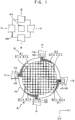
- FIG. 1 is a plan view schematically illustrating an exemplary embodiment of a display device.
- FIG. 2 is a plan view schematically illustrating areas of a first substrate of the display panel of FIG. 1 .
- FIG. 3 is a cross-sectional view illustrating a portion of the display device of FIG. 1 .
- FIG. 4 is a circuit diagram conceptually illustrating a unit pixel of the display panel of FIG. 1 .
- the display device may include a display panel PN displaying an image, a controller board 800 for controlling the display panel PN, a first flexible circuit film 410, a second flexible circuit film 510, a third flexible circuit film 610, a fourth flexible circuit film 710, and a backlight unit BLU disposed below the display panel PN to provide the display panel PN with light.
- the first to fourth flexible circuit film 410, 510, 610 and 710 connect to the display panel PN and the controller board 800.
- the controller board 800 may be disposed below the backlight unit BLU.
- the controller board 800 may include a timing controller 810.
- the timing controller 810 converts an image signal applied from an external device (not shown) into an image control signal for controlling the display panel PN.
- the display panel PN may include a first substrate 100, a second substrate 200 facing the first substrate 100 and a liquid crystal layer 300 interposed between the first substrate 100 and the second substrate 200.
- the first substrate 100 may include a base substrate 110, a gate line portion GL, a gate insulation layer 120, a data line portion DL, a plurality of thin-film transistors (TFTs) 130, a protective layer 140 and a plurality of pixel electrodes 150.
- TFTs thin-film transistors
- the gate line portion GL may include a plurality of gate lines formed on the base substrate 110 to be extended along a first direction DI1.
- the gate insulation layer 120 may be formed on the base substrate 110 to cover the gate line portion GL.
- the data line portion DL may be formed on the gate insulation layer 120 to have a plurality of data lines being extended in a second direction DI2 crossing the first direction DI1.
- the first and second directions DI1 and DI2 may be substantially perpendicular to each other.
- Each of the TFTs 130 may be connected to one of the gate lines to receive a gate signal, and may be connected to one of the data lines to receive a data signal.
- the protective layer 140 may be formed on the gate insulation layer 120 to cover the data line DL and the TFTs 130.
- the pixel electrodes 150 may be formed on the protective layer 140 in a matrix shape, and may be electrically connected to the TFTs 130 through a contact hole formed through the protective layer 140.
- a TFT 130 and a pixel electrode 150 formed on a unit pixel area may define a pixel part.
- the second substrate 200 may include an opposite base substrate 210, a light-blocking pattern 220, a plurality of color filters 230, an organic insulation layer 240 and a common electrode 250.
- the opposite base substrate 210 may be disposed to face the base substrate 110 of the first substrate 100.
- the light-blocking pattern 220 may be formed on the opposite base substrate 210 to cover the gate line portion GL, the data line portion DL and the TFTs 130.
- the color filters 230 may be formed on the opposite base substrate 210 so as to correspond to the pixel electrodes 150.
- the color filters 230 may include red color filters R, green color filters G and blue color filters B.
- the organic insulation layer 240 may cover the light-blocking pattern 220 and the color filters 230 to planarize a surface of the light-blocking pattern 220 and the color filters 230.
- the common electrode 250 may be formed on the organic insulation layer 240 to receive a common voltage Vcom from an external device (not shown).
- the arrangement of liquid crystals in the liquid crystal layer 300 is altered by an electric field formed between the pixel electrodes 150 and the common electrode 250, and thus the transmissivity of light through the liquid crystal layer 300 is changed.
- the base substrate 110 may include a display area displaying an image and a peripheral area surrounding the display area.
- the display area has a circular shape
- the peripheral area has a ring shape surrounding peripheral portions of the display area.
- the display area is divided into four areas by first and second lines that are substantially perpendicular to each other. That is, the display area may include a first divided display area DA1, a second divided display area DA2, a third divided display area DA3 and a fourth divided display area DA4 that are sequentially disposed along a clockwise direction.
- the first to fourth divided display areas DA1, DA2, DA3 and DA4 may have substantially the same size.
- the peripheral area may include a first peripheral area PEA1, a second peripheral area PEA2, a third peripheral area PEA3 and a fourth peripheral area PEA4 formed at peripheral portions of the first to fourth divided display areas DA1, DA2, DA3 and DA4, respectively. All of the first and fourth peripheral areas PEA1, PEA2, PEA3 and PEA4 may be extended along the peripheral portions of the display area. In an embodiment, the first to fourth peripheral areas PEA1, PEA2, PEA3 and PEA4 may have substantially the same size.
- the peripheral area may further include a first protruding area PA1 extended from the first peripheral area PEA1 in the outward direction thereof, a second protruding area PA2 extended from the second peripheral area PEA2 in the outward direction thereof, a third protruding area PA3 extended from the third peripheral area PEA3 in the outward direction thereof, and a fourth protruding area PA4 extended from the fourth peripheral area PEA4 in the outward direction thereof.
- the first protruding area PA1 is disposed adjacent to the fourth peripheral area PEA4, the second protruding area PA2 is disposed adjacent to the first peripheral area PEA1, the third protruding area PA3 is disposed adjacent to the second peripheral area PEA2, and the fourth protruding area PA4 is disposed adjacent to the third peripheral area PEA3.
- the first to fourth protruding areas PA1, PA2, PA3 and PA4 may have substantially the same shape, and may have substantially the same size.
- the gate line portion GL may include a plurality of first gate lines GL1 and a plurality of second gate lines GL2.
- the first gate lines GL1 may be formed on the first and second divided display areas DA1 and DA2 substantially parallel with the first direction DI1, and may be extended on the first peripheral area PEA1.
- the second gate lines GL2 be formed on the third and fourth divided display areas DA3 and DA4 substantially parallel with the first direction DI1, and may be extended on the third peripheral area PEA3.
- the first gate lines GL1 may include a plurality of first gate main lines GL1-a and a plurality of first gate peripheral lines GL1-b.
- the first gate main lines GL1-a are formed on the first and second divided display areas DA1 and DA2 substantially parallel with the first direction DI1.
- the first gate peripheral lines GL1-b are formed on the first peripheral area PEA1 to be connected to a terminal of the first gate main lines GL1-a, respectively.
- the first gate peripheral lines GL1-b may be formed along a length direction of the first peripheral area PEA1, and may be further extended outwardly on the first protruding area PA1.
- the second gate lines GL2 may include a plurality of second gate main lines GL2-a and a plurality of second gate peripheral lines GL2-b.
- the second gate main lines GL2-a are formed on the third and fourth divided display areas DA3 and DA4 substantially parallel with the first direction DI1.
- the second gate peripheral lines GL2-b are formed on the third peripheral area PEA3 to be connected to a terminal of the second gate main lines GL2-a, respectively.
- the second gate peripheral lines GL2-b may be formed along a length direction of the third peripheral area PEA3, and may be further extended outwardly on the third protruding area PA3.
- the data line portion DL may include a plurality of first data lines DL1 and a plurality of second data lines DL2.
- the first data lines DL1 may be formed on the fourth and first divided display areas DA4 and DA1 substantially parallel with the second direction DI2, and may be extended on the fourth peripheral area PEA4.
- the second data lines DL2 may be formed on the second and third divided display areas DA2 and DA3 substantially parallel with the second direction DI2, and may be extended on the second peripheral area PEA2.
- the first data lines DL1 may include a plurality of first data main lines DL1-a and a plurality of first data peripheral lines DL1-b.
- the first data main lines DL1-a are formed on the first and fourth divided display areas DA1 and DA4 substantially parallel with the second direction DI2.
- the first data peripheral lines DL1-b are formed on the fourth peripheral area PEA4 to be connected to a terminal of the first data main lines DL1-a respectively.
- the first data peripheral lines DL1-b may be formed along a length direction of the fourth peripheral area PEA4, and may be further extended outwardly on the fourth protruding area PA4.
- the second data lines DL2 may include a plurality of second data main lines DL2-a and a plurality of second data peripheral lines DL2-b.
- the second data main lines are formed on the second and third divided display areas DA2 and DA3 substantially parallel with the second direction DI2.
- the second data peripheral lines DL2-b are formed on the second peripheral area PEA2 to be connected to a terminal of the second data main lines DL2-a, respectively.
- the second data peripheral lines DL2-b may be formed along a length direction of the second peripheral area PEA2, and may be further extended outwardly on the second protruding area PA2.
- the first gate peripheral lines GL1-b, the second gate peripheral lines GL2-b, the first data peripheral lines DL1-b and the second data peripheral lines DL2-b are extended in a direction identical to a clockwise direction or a counterclockwise direction.
- the first flexible circuit film 410 is attached on the first protruding area PA1 to be electrically connected to the first gate peripheral lines GL1-b.
- the first flexible circuit film 410 may be electrically connected to the first gate peripheral lines GL1-b by first gate pad parts (not shown) and a first anisotropic conductive film (not shown) formed on a terminal of the first gate peripheral lines GL1-b.
- the second flexible circuit film 510 is attached on the third protruding area PA3 to be electrically connected to the second gate peripheral lines GL2-b.
- the second flexible circuit film 510 may be electrically connected to the second gate peripheral lines GL2-b by second gate pad parts (not shown) and a second anisotropic conductive film (not shown) formed on a terminal of the second gate peripheral lines GL2-b.
- the third flexible circuit film 610 is attached on the fourth protruding area PA4 to be electrically connected to the first data peripheral lines DL1-b.
- the third flexible circuit film 610 may be electrically connected to the first data peripheral lines DL1-b by first data pad parts (not shown) and a third anisotropic conductive film (not shown) formed on a terminal of the first data peripheral lines DL1-b.
- the fourth flexible circuit film 710 is attached on the second protruding area PA2 to be electrically connected to the second data peripheral lines DL2-b.
- the fourth flexible circuit film 710 may be electrically connected to the second data peripheral lines DL2-b by second data pad parts (not shown) and a fourth anisotropic conductive film (not shown) formed on a terminal of the second data peripheral lines DL2-b.
- the display panel PN may further include a first gate driving part 400, a second gate driving part 500, a first data driving part 600 and a second data driving part 700.
- the first gate driving part 400 having a chip form is mounted on the first flexible circuit film 410 to receive the image controlling signal from the controller board 800.
- the first gate driving part 400 generates first gate signals in response to the image controlling signal, and applies the first gate signals to each of the first gate lines GL1.
- the second gate driving part 500 is mounted on the second flexible circuit film 510 in a chip form to receive the image controlling signal from the controller board 800.
- the second gate driving part 500 generates second gate signals in response to the image controlling signal, and applies the second gate signals to each of the second gate lines GL2.
- the first data driving part 600 is mounted on the third flexible circuit film 610 in a chip form to receive the image controlling signal from the controller board 800.
- the first data driving part 600 generates first data signals in response to the image controlling signal, and applies the first data signals to each of the first data lines DL1.
- the second data driving part 700 is mounted on the fourth flexible circuit film 710 in a chip form to receive the image controlling signal from the controller board 800.
- the second data driving part 700 generates second data signals in response to the image controlling signal, and applies to each of the second data lines DL2.
- the first and second gate driving parts 400 and 500, and the first and second data driving parts 600 and 700 are mounted on the first to fourth flexible circuit films 410, 510, 610 and 710, respectively.
- the first and second gate driving parts 400 and 500, and the first and second data driving parts 600 and 700 may be mounted on the first substrate 100. That is, the first gate driving part 400 is mounted on the first protruding area PA1 to be electrically connected to the first gate peripheral lines GL1-b.
- the second gate driving part 500 is mounted on the third protruding area PA3 to be electrically connected to the second gate peripheral lines GL2-b.
- the first data driving part 600 is mounted on the fourth protruding area PA4 to be electrically connected to the first data peripheral lines DL1-b.
- the second data driving part 700 is mounted on the second protruding area PA2 to be electrically connected to the second gate peripheral lines DL2-b.
- the display area having a circular shape is divided into four areas, that is, the first to fourth divided display areas DA1, DA2, DA3 and DA4.
- the first to fourth peripheral areas PEA1, PEA2, PEA3 and PEA4 are formed on the peripheral portions of each the first to fourth divided display areas DA1, DA2, DA3 and DA4.
- the first gate lines GL1 are formed on the first and second divided display areas DA1 and DA2 and the first peripheral area PEA1 to be driven by the first gate driving part 400.
- the second gate lines GL2 are formed on the third and fourth divided display areas DA3 and DA4 and the third peripheral area PEA3 to be driven by the second gate driving part 500.
- the first data lines DL1 are formed on the first and fourth divided display areas DA1 and DA4 and the fourth peripheral area PEA4 to be driven by the first data driving part 600.
- the second data lines DL2 is formed on the second and third divided display areas DA2 and DA3 and the second peripheral area PEA2 to be driven by the second data driving part 700.
- the display panel PN may display an image of a circular shape.
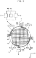
- FIG. 5 is a plan view schematically illustrating the display device according to the present invention.
- the display device of this embodiment is substantially identical to the previous embodiment of the display device described in connection with FIGS. 1 to 4 , except for the omission of the first and second flexible circuit films 410 and 510. Accordingly, the same reference numerals will be used to refer to the same elements as those described, and detailed explanation thereof may be omitted.
- the first and second gate driving parts 400 and 500 are formed on the base substrate 110 by a process substantially identical to the TFTs 130.
- the first gate driving parts 400 are formed on the first protruding area PA1 to be electrically connected to the first gate peripheral lines GL1-b.
- the first gate driving parts 400 may include a first driving TFTs (not shown) formed by a process substantially identical to the TFTs 130.
- the second gate driving parts 500 are formed on the third protruding area PA3 to be electrically connected to the second gate peripheral lines GL2-b.
- the second gate driving parts 500 may include a second driving TFTs (not shown) formed by a process substantially identical to the TFTs 130.
- the first gate driving part 400 may be electrically connected to the second data driving part 700 by a first gate control line 10 formed on the first peripheral area PEA1.
- the second gate driving part 500 may be electrically connected to the first data driving part 600 by a second gate control line 20 formed on the third peripheral area PEA3.
- the first gate driving part 400 may be driven by the second data driving part 700.
- the second gate driving part 500 may be driven by the first data driving part 600.
- first gate driving part 400 may be electrically connected to the first data driving part 700 to be controlled.
- the second gate driving part 500 may be electrically connected to the second data driving part 600 to be controlled.
- first and second gate driving parts 400 and 500 are formed on the base substrate 110, manufacturing costs and the volume of the display device may be reduced.
- FIG. 6 is a plan view schematically illustrating an exemplary embodiment of a display device.
- the display device in this embodiment is substantially identical to the previous embodiment of the display device described in conjunction with FIGS. 1 to 4 , except for the shape of the base substrate 110. Accordingly, the same reference numerals will be used to refer to the same elements as those described, and detailed explanation thereon may be omitted.
- the base substrate 110 may have various shapes other than a circular shape as shown in FIG. 1 . That is, a display area of the base substrate 110 may have various shapes other than a circular shape. In an embodiment, the display area may have a symmetrical shape with respect to the first and second directions DI1 and DI2. In exemplary embodiments, the display area may have an oval shape, a polygonal shape, a star shape, a heart shape, and the like. In an embodiment, a display area may have an octagonal shape as shown in FIG. 6 .
- All of the first to fourth peripheral areas PEA1, PEA2, PEA3 and PEA4 may be extended along the peripheral portions of the display area.
- the display panel PN may display an image having various shapes other than a circular shape.
- FIG. 7 is a plan view schematically illustrating an exemplary embodiment of a display device.
- the display device in this embodiment is substantially identical to the previous embodiment of the display device described in connection with FIGS. 1 to 4 , except for positions of the first to fourth protruding areas PA1, PA2, PA3 and PA4. Accordingly, the same reference numerals will be used to refer to the same elements as those described, and detailed explanation thereon may be omitted.
- the first protruding area PA1 may be disposed at any position in the first peripheral area PEA1 that are not adjacent to the fourth peripheral area PEA4 and the second peripheral area PEA2. Accordingly, a portion of the first gate peripheral lines GL1-b is extended in a clockwise direction, and the remaining portion of the first gate peripheral lines GL1-b is extended in a counterclockwise direction. In an embodiment, the number of the clockwise first gate peripheral lines GL1-b is equal to that of the counterclockwise first gate peripheral lines GL1-b.
- the first protruding area PA1 is disposed at a middle position of the first peripheral area PEA1 that are not adjacent to the fourth peripheral area PEA4 and the second peripheral area PEA2. That is, the first gate peripheral lines GL1-b is formed on the first protruding area PA1 in a peripheral direction, and is extended along a length direction of the first peripheral area PEA1 in a clockwise direction and a counterclockwise direction with respect to the first protruding area PA1 to be connected to the first gate main lines GL1-a.
- the third protruding area PA3 may be disposed at any position in the third peripheral area PEA3 that are not adjacent to the second peripheral area PEA2 and the fourth peripheral area PEA4. Accordingly, a portion of the second gate peripheral lines GL2-b is extended in a clockwise direction, and the remaining portion of the second gate peripheral lines GL2-b is extended in a counterclockwise direction. In an embodiment, the number of the clockwise second gate peripheral lines GL2-b is equal to that of the counterclockwise second gate peripheral lines GL2-b.
- the third protruding area PA3 is disposed at a middle position of the third peripheral area PEA3 that are not adjacent to the second peripheral area PEA2 and the fourth peripheral area PEA4. That is, the second gate peripheral lines GL2-b is formed on the third protruding area PA3 in a peripheral direction, and is extended along a length direction of the third peripheral area PEA3 in a clockwise direction and a counterclockwise direction with respect to the third protruding area PA3 to be connected to the second gate main lines GL2-a.
- the fourth protruding area PA4 may be disposed at any position in the fourth peripheral area PEA4 that are not adjacent to the first peripheral area PEA1 and the third peripheral area PEA3., Accordingly, a portion of the first data peripheral lines DL1-b is extended in a clockwise direction, and the remaining portion of the first data peripheral lines DL1-b is extended in a counterclockwise direction. In an embodiment, the number of the clockwise first data peripheral lines DL1-b is equal to that of the counterclockwise first data peripheral lines DL1-b.
- the fourth protruding area PA4 is disposed at a middle position of the fourth peripheral area PEA4 that are not adjacent to the first peripheral area PEA1 and the third peripheral area PEA3. That is, the first data peripheral lines DL1-b is formed on the fourth protruding area PA4 in a peripheral direction, and is extended along a length direction of the fourth peripheral area PEA4 in a clockwise direction and a counterclockwise direction with respect to the fourth protruding area PA4 to be connected to the first data main lines DL1-a.
- the second protruding area PA2 may be disposed at any position in the second peripheral area PEA2 that are not adjacent to the first peripheral area PEA1 and the third peripheral area PEA3. Accordingly, a portion of the second data peripheral lines DL2-b is extended in a clockwise direction, and the remaining portion of the second data peripheral lines DL2-b is extended in a counterclockwise direction. In an embodiment, the number of the clockwise second data peripheral lines DL2-b is equal to that of the counterclockwise second gate peripheral lines DL2-b.
- the second data peripheral lines DL2-b is formed on the second protruding area PA2 in a peripheral direction, and is extended along a length direction of the second peripheral area PEA2 in a clockwise direction and a counterclockwise direction with respect to the second protruding area PA2 to be connected to the second data main lines DL2-a.
- the widths of the first to fourth peripheral areas PEA1, PEA2, PEA3 and PEA4 may be reduced.
- FIG. 8 is a plan view schematically illustrating an exemplary embodiment of a display device.
- the display device in this embodiment is substantially identical to the previous embodiment of the display device described in connection with FIGS. 1 to 4 , except for the structure of the protruding areas, and their associated configurations of the gate and data driving parts and the flexible circuit films, and the like. Accordingly, the same reference numerals will be used to refer to the same elements as those described, and detailed explanation thereon may be omitted.
- the first and fourth protruding areas PA1 and PA4 are integrated into a first integrated protruding area PA14, and the second and third protruding areas PA2 and PA3 are integrated into a second integrated protruding area PA23.
- the first gate peripheral lines GL1-b is formed on the first peripheral area PEA1 in a counterclockwise direction with respect to the first integrated protruding area PA14, and is outwardly extended to the first integrated protruding area PA14.
- the second gate peripheral lines GL2-b is formed on the fourth peripheral area PEA4 in a clockwise direction with respect to the second integrated protruding area PA23, and is outwardly extended to the second integrated protruding area PA23.
- a side of the first flexible circuit film FP1 is attached on the first integrated protruding areas PA14 to be electrically connected to the first gate peripheral lines GL1-b and the first data peripheral lines DL1-b. Another side of the first flexible circuit film FP1 is attached on the controller board 800 to be electrically connected.
- a side of the second flexible circuit film FP2 is attached on the second integrated protruding areas PA23 to be electrically connected to the second gate peripheral lines GL2-b and the second data peripheral lines DL2-b. Another side of the second flexible circuit film FP2 is attached on the controller board 800 to be electrically connected.
- the first integrated driving chip TIC1 is mounted on the first flexible circuit film FP1 to receive the image controlling signal from the controller board 800.
- the first integrated driving chip TIC1 responds to the image controlling signal to generate first gate signals and first data signals.
- the first gate signals are applied to the first gate peripheral lines GL1-b through the first flexible circuit film FP1, respectively.
- the first data signals are applied to the first data peripheral lines DL1-b through the first flexible circuit film FP1, respectively.
- the first integrated driving chip TIC1 is a driving chip integrating the first gate driving part 400 and the first data driving part 600 in the previous embodiment shown in FIGS. 1 to 4 .
- the second integrated driving chip TIC2 is mounted on the second flexible circuit film FP2 to receive the image controlling signal from the controller board 800.
- the second integrated driving chip TIC2 responds to the image controlling signal to generate second gate signals and second data signals.
- the second gate signals are applied to the second gate peripheral lines GL2-b through the second flexible circuit film FP2, respectively.
- the second data signals are applied to the second data peripheral lines DL2-b through the second flexible circuit film FP2, respectively.
- the second integrated driving chip TIC2 is a driving chip integrating the second gate driving part 500 and the second data driving part 700 in the previous embodiment of FIGS. 1 to 4 .
- the first and second integrated driving chips TIC1 and TIC2 are formed on the first and second flexible circuit films FP1 and FP2, respectively.
- the first integrated driving chips TIC1 may be mounted on the first and fourth protruding areas PA1 and PA4 that are integrated to each other to be electrically connected to the first gate peripheral lines GL1-b and the first data peripheral lines DL1-b.
- the second integrated driving chips TIC2 may be mounted on the second and third protruding areas PA2 and PA3 that are integrated to each other to be electrically connected to the second gate peripheral lines GL2-b and the second data peripheral lines DL2-b.
- first and fourth protruding areas PA1 and PA4 are connected to each other to be integrally formed, and the second and third protruding areas PA2 and PA3 are connected to each other to be integrally formed.
- first and second protruding areas PA1 and PA2 may be connected to each other to be integrally formed, and the third and fourth protruding areas PA3 and PA4 may be connected to each other to be integrally formed.
- the first integrated driving chip TIC1 integrates the first gate driving part 400 and the second data driving part 700
- the second integrated driving chip TIC2 integrates the second gate driving part 500 and the first data driving part 600. Accordingly, manufacturing costs and the volume of the display device may be reduced.
- a display area displaying an image and a peripheral area surrounding the display area are divided into four areas. Gate lines or the data lines are formed on each area. Accordingly, a first substrate of a display panel may have various shapes other than a rectangle. Thus, the display panel may display an image having various shapes other than a rectangular.
Landscapes
- Physics & Mathematics (AREA)
- Nonlinear Science (AREA)
- General Physics & Mathematics (AREA)
- Chemical & Material Sciences (AREA)
- Crystallography & Structural Chemistry (AREA)
- Optics & Photonics (AREA)
- Mathematical Physics (AREA)
- Engineering & Computer Science (AREA)
- Microelectronics & Electronic Packaging (AREA)
- Theoretical Computer Science (AREA)
- Computer Hardware Design (AREA)
- Devices For Indicating Variable Information By Combining Individual Elements (AREA)
- Liquid Crystal (AREA)
Claims (8)
- Anzeigevorrichtung mit einem Anzeigeträger und einer Anzeigetafel, wobei der Anzeigeträger umfasst:einen Basisträger, umfassend:einen Anzeigebereich, der in einen ersten geteilten Anzeigebereich (DA1), einen zweiten geteilten Anzeigebereich (DA2), einen dritten geteilten Anzeigebereich (DA3) und einen vierten geteilten Anzeigebereich (DA4) geteilt ist, die nacheinander im Uhrzeigersinn angeordnet sind; undeinen Randbereich, der an einem Randabschnitt des Anzeigebereichs angeordnet ist;einen Gate-Leitungsabschnitt, umfassend:erste Gate-Hauptleitungen (GL1-a), die auf dem ersten und zweiten geteilten Anzeigebereich (DA1, DA2) im Wesentlichen parallel zu einer ersten Richtung angeordnet sind; undzweite Gate-Hauptleitungen (GL2-a), die auf dem dritten und vierten geteilten Bereich (DA3, DA4) im Wesentlichen parallel zu der ersten Richtung angeordnet sind;einen Datenleitungsabschnitt, umfassend:erste Datenhauptleitungen (DL1-a), die auf dem vierten und ersten geteilten Anzeigebereich (DA4, DA1) im Wesentlichen parallel zu einer zweiten Richtung angeordnet sind, die im Wesentlichen senkrecht zu der ersten Richtung ist; undzweite Datenhauptleitungen (DL2-a), die auf dem zweiten und dritten geteilten Anzeigebereich (DA2, DA3) im Wesentlichen parallel zu der zweiten Richtung angeordnet sind; undPixelabschnitte, die in dem Anzeigebereich in einem Matrixmuster angeordnet sind, wobei die Pixelabschnitte elektrisch mit den ersten und zweiten Gate-Hauptleitungen und den ersten und zweiten Datenhauptleitungen verbunden sind, wobei der Randbereich einen ersten Randbereich (PEA1), einen zweiten Randbereich (PEA2), einen dritten Randbereich (PEA3) und einen vierten Randbereich (PEA4) beinhaltet, die jeweils dem ersten bis vierten geteilten Anzeigebereich entsprechen;wobei die Anzeigetafel (PN) ferner ein erstes Gate-Treiberteil (400), ein zweites Gate-Treiberteil (500), ein erstes Datentreiberteil (600) und ein zweites Datentreiberteil (700) beinhaltet;gekennzeichnet durch die folgenden Merkmale:
das erste Gate-Treiberteil (400) ist elektrisch mit dem zweiten Datentreiberteil (700) durch eine erste Gate-Steuerleitung (10) verbunden, die auf dem ersten Randbereich (PEA1) ausgebildet ist, das zweite Gate-Treiberteil (500) ist elektrisch mit dem ersten Datentreiberteil (600) durch eine zweite Gate-Steuerleitung (20) verbunden, die auf dem dritten Randbereich (PEA3) ausgebildet ist, sodass das erste Gate-Treiberteil (400) durch das zweite Datentreiberteil (700) angesteuert wird und das zweite Gate-Treiberteil (500) durch das erste Datentreiberteil (600) angesteuert wird. - Anzeigevorrichtung nach Anspruch 1, wobei
die Anzeigevorrichtung beinhaltet:eine Steuerplatine (800) zum Steuern der Anzeigetafel (PN), eine erste flexible Schaltungsfolie (610), eine zweite flexible Schaltungsfolie (710), wobei die flexiblen Schaltungsfolien (610, 710) mit der Anzeigetafel (PN) und der Steuerplatine (800) verbunden sind,eine Hintergrundbeleuchtungseinheit (BLU), die unter der Anzeigetafel (PN) angeordnet ist, um die Anzeigetafel (PN) mit Licht zu versorgen. - Anzeigeträger nach Anspruch 1, wobei der Gate-Leitungsabschnitt ferner umfasst:erste Gate-Randleitungen (GL1-b), die mit Anschlüssen der ersten Gate-Hauptleitungen verbunden sind, wobei die ersten Gate-Randleitungen (GL1-b) auf dem Randbereich angeordnet sind; undzweite Gate-Randleitungen (GL2-b), die mit Anschlüssen der zweiten Gate-Hauptleitungen verbunden sind, wobei die zweiten Gate-Randleitungen (GL2-b) auf dem Randbereich angeordnet sind, wobei der Datenleitungsabschnitt ferner umfasst:erste Datenrandleitungen (DL1-b), die mit Anschlüssen der ersten Datenhauptleitungen verbunden sind, wobei die ersten Datenrandleitungen (DL1-b) auf dem Randbereich angeordnet sind; undzweite Datenrandleitungen (DL2-b), die mit Anschlüssen der zweiten Datenhauptleitungen verbunden sind, wobei die zweiten Datenrandleitungen (DL2-b) auf dem Randbereich angeordnet sind.
- Anzeigeträger nach Anspruch 3, wobei sich die ersten Gate-Randleitungen (GL1 - b) in einer Längsrichtung des Randbereichs erstrecken,
sich die zweiten Gate-Randleitungen (GL2-b) in einer Längsrichtung des Randbereichs erstrecken,
sich die ersten Datenrandleitungen (DL1-b) in einer Längsrichtung des Randbereichs erstrecken; und
sich die zweiten Datenrandleitungen (DL2-b) in einer Längsrichtung des Randbereichs erstrecken. - Anzeigeträger nach Anspruch 4, wobei sich die ersten und zweiten Gate-Randleitungen (GL1-b, GL2-b) und die ersten und zweiten Datenrandleitungen (DL1-b, DL2-b) im gleichen Uhrzeigersinn bzw. Gegenuhrzeigersinn im Randbereich erstrecken.
- Anzeigeträger nach Anspruch 3, wobei
sich die ersten Gate-Randleitungen (GL1-b) und die ersten Datenrandleitungen (DL1-b) in entgegengesetzte Richtungen voneinander erstrecken und
sich die zweiten Gate-Randleitungen (GL2-b) und die zweiten Datenrandleitungen (DL2-b) in entgegengesetzte Richtungen voneinander erstrecken. - Anzeigeträger nach Anspruch 1, wobei der Anzeigebereich eines aus einer runden Form und einer vieleckigen Form aufweist.
- Anzeigeträger nach Anspruch 1, wobei der Anzeigebereich eine symmetrische Form in Bezug auf die erste und zweite Richtung aufweist.
Applications Claiming Priority (1)
| Application Number | Priority Date | Filing Date | Title |
|---|---|---|---|
| KR1020080120856A KR101535929B1 (ko) | 2008-12-02 | 2008-12-02 | 표시기판, 이를 갖는 표시패널 및 이를 갖는 표시장치 |
Publications (3)
| Publication Number | Publication Date |
|---|---|
| EP2194425A2 EP2194425A2 (de) | 2010-06-09 |
| EP2194425A3 EP2194425A3 (de) | 2012-04-11 |
| EP2194425B1 true EP2194425B1 (de) | 2018-09-12 |
Family
ID=41136827
Family Applications (1)
| Application Number | Title | Priority Date | Filing Date |
|---|---|---|---|
| EP09009612.4A Active EP2194425B1 (de) | 2008-12-02 | 2009-07-24 | Anzeigeträger, Anzeigetafel mit dem Anzeigeträger und Anzeigevorrichtung mit der Anzeigetafel |
Country Status (3)
| Country | Link |
|---|---|
| US (2) | US8432523B2 (de) |
| EP (1) | EP2194425B1 (de) |
| KR (1) | KR101535929B1 (de) |
Families Citing this family (56)
| Publication number | Priority date | Publication date | Assignee | Title |
|---|---|---|---|---|
| KR20140109261A (ko) * | 2013-03-05 | 2014-09-15 | 가부시키가이샤 한도오따이 에네루기 켄큐쇼 | 표시 장치 및 전자 기기 |
| CN106463082B (zh) * | 2014-06-23 | 2019-07-16 | 株式会社半导体能源研究所 | 显示装置及电子设备 |
| KR102295874B1 (ko) * | 2014-07-24 | 2021-08-31 | 엘지디스플레이 주식회사 | 디스플레이 장치 |
| WO2016021512A1 (ja) * | 2014-08-06 | 2016-02-11 | シャープ株式会社 | 表示装置およびこれを備えた装置 |
| KR102253455B1 (ko) * | 2014-08-25 | 2021-05-20 | 삼성디스플레이 주식회사 | 표시 패널 |
| KR102313861B1 (ko) * | 2014-09-03 | 2021-10-18 | 엘지디스플레이 주식회사 | 웨어러블 디바이스 |
| TWI518650B (zh) * | 2014-10-27 | 2016-01-21 | 群創光電股份有限公司 | 顯示裝置 |
| KR102244072B1 (ko) * | 2014-10-30 | 2021-04-26 | 삼성디스플레이 주식회사 | 표시 장치 |
| US9780157B2 (en) * | 2014-12-23 | 2017-10-03 | Lg Display Co., Ltd. | Flexible display device with gate-in-panel circuit |
| KR102342868B1 (ko) * | 2014-12-31 | 2021-12-23 | 삼성디스플레이 주식회사 | 비사각형 디스플레이 및 그 구동 방법 |
| KR102315671B1 (ko) | 2015-01-19 | 2021-10-21 | 삼성디스플레이 주식회사 | 표시 장치 |
| US9678588B2 (en) | 2015-01-28 | 2017-06-13 | Sony Corporation | Wire-bonded borderless display |
| KR20160095311A (ko) * | 2015-02-02 | 2016-08-11 | 삼성디스플레이 주식회사 | 유기 발광 표시 장치 |
| KR102370353B1 (ko) | 2015-02-13 | 2022-03-07 | 삼성디스플레이 주식회사 | 디스플레이 장치 |
| KR102544696B1 (ko) * | 2015-02-16 | 2023-06-16 | 삼성디스플레이 주식회사 | 원형 터치 패널 및 그 제조 방법 |
| JP6154086B2 (ja) * | 2015-03-10 | 2017-06-28 | シャープ株式会社 | 表示装置 |
| US10036909B2 (en) * | 2015-03-10 | 2018-07-31 | Sharp Kabushiki Kaisha | Display device |
| US10067583B2 (en) | 2015-03-31 | 2018-09-04 | Sony Corporation | Virtual borderless display |
| US10204535B2 (en) | 2015-04-06 | 2019-02-12 | Semiconductor Energy Laboratory Co., Ltd. | Display device and electronic device |
| US9547208B2 (en) * | 2015-04-27 | 2017-01-17 | Sony Corporation | Divided backlight configuration of a display |
| KR102293411B1 (ko) * | 2015-05-08 | 2021-08-25 | 삼성디스플레이 주식회사 | 비사각형 디스플레이 |
| KR102519819B1 (ko) * | 2015-05-28 | 2023-04-12 | 엘지디스플레이 주식회사 | 표시장치 |
| US9940866B2 (en) * | 2015-06-01 | 2018-04-10 | Apple Inc. | Electronic device having display with curved edges |
| KR102354970B1 (ko) * | 2015-06-22 | 2022-01-25 | 삼성디스플레이 주식회사 | 디스플레이 장치 |
| KR102342556B1 (ko) | 2015-07-31 | 2021-12-23 | 엘지전자 주식회사 | 반도체 발광 소자를 이용한 디스플레이 장치 |
| CN105096804B (zh) * | 2015-08-28 | 2018-06-01 | 友达光电股份有限公司 | 显示面板 |
| US20180286316A1 (en) * | 2015-09-11 | 2018-10-04 | Sharp Kabushiki Kaisha | Display device and circuit member |
| KR102483379B1 (ko) * | 2015-09-21 | 2023-01-02 | 삼성디스플레이 주식회사 | 표시장치 |
| CN105137687B (zh) * | 2015-09-29 | 2019-05-28 | 京东方科技集团股份有限公司 | 阵列基板及其制作方法、显示装置 |
| US10162311B2 (en) * | 2015-12-15 | 2018-12-25 | Qualcomm Incorporated | Display panel with minimum borders |
| EP3907729B1 (de) | 2016-01-21 | 2025-02-26 | Apple Inc. | Leistungs- und datenroutingstrukturen für anzeigen mit organischen leuchtdioden |
| JP2017134338A (ja) | 2016-01-29 | 2017-08-03 | 株式会社ジャパンディスプレイ | 表示装置 |
| JP6689088B2 (ja) * | 2016-02-08 | 2020-04-28 | 株式会社ジャパンディスプレイ | 表示装置 |
| CN107305757A (zh) * | 2016-04-21 | 2017-10-31 | 瀚宇彩晶股份有限公司 | 显示装置 |
| KR102654508B1 (ko) | 2016-05-04 | 2024-04-04 | 삼성디스플레이 주식회사 | 표시 장치 |
| KR102581759B1 (ko) * | 2016-05-23 | 2023-09-25 | 삼성디스플레이 주식회사 | 표시 장치 |
| JP6773277B2 (ja) * | 2016-08-05 | 2020-10-21 | 天馬微電子有限公司 | 表示装置 |
| KR20180018930A (ko) * | 2016-08-11 | 2018-02-22 | 삼성디스플레이 주식회사 | 표시장치 및 그의 구동방법 |
| US10409102B2 (en) * | 2016-09-08 | 2019-09-10 | Japan Display Inc. | Display device |
| CN107807480B (zh) * | 2016-09-08 | 2021-04-20 | 株式会社日本显示器 | 显示装置 |
| CN108073003B (zh) | 2016-11-09 | 2020-08-18 | 元太科技工业股份有限公司 | 显示面板、像素阵列衬底与线路阵列结构 |
| US10475371B2 (en) | 2016-11-14 | 2019-11-12 | Int Tech Co., Ltd. | Pixel circuit in an electroluminescent display |
| KR102619425B1 (ko) | 2016-11-21 | 2023-12-29 | 엘지디스플레이 주식회사 | 표시장치 |
| JP2019070744A (ja) * | 2017-10-10 | 2019-05-09 | 三菱電機株式会社 | 液晶表示装置 |
| CN108447390B (zh) * | 2018-02-27 | 2020-07-03 | 上海天马微电子有限公司 | 环形显示模组和显示装置 |
| KR101883890B1 (ko) * | 2018-03-13 | 2018-08-01 | 엘지디스플레이 주식회사 | 디스플레이 장치 |
| CN110349547A (zh) * | 2018-04-03 | 2019-10-18 | 群创光电股份有限公司 | 显示装置 |
| CN108389516B (zh) * | 2018-05-14 | 2021-06-29 | 昆山国显光电有限公司 | 异形显示屏及显示装置 |
| KR20200046913A (ko) | 2018-10-26 | 2020-05-07 | 엘지디스플레이 주식회사 | 링크 배선의 구조 및 이를 이용한 표시패널 |
| CN109712558A (zh) * | 2019-03-19 | 2019-05-03 | 成都京东方光电科技有限公司 | 异形显示面板、显示装置 |
| KR102715253B1 (ko) * | 2019-10-10 | 2024-10-10 | 엘지디스플레이 주식회사 | 디스플레이 장치 및 구동 방법 |
| JP6995917B2 (ja) * | 2020-04-07 | 2022-01-17 | 株式会社ジャパンディスプレイ | 表示装置 |
| WO2021237725A1 (zh) | 2020-05-29 | 2021-12-02 | 京东方科技集团股份有限公司 | 显示基板和显示装置 |
| US12525161B2 (en) | 2022-04-28 | 2026-01-13 | E Ink Holdings Inc. | Narrow border reflective display device |
| US20230386387A1 (en) * | 2022-05-31 | 2023-11-30 | Innolux Corporation | Modulating device |
| US20260112327A1 (en) * | 2022-09-23 | 2026-04-23 | Fuzhou Boe Optoelectronics Technology Co., Ltd. | Display Panel and Display Module |
Family Cites Families (8)
| Publication number | Priority date | Publication date | Assignee | Title |
|---|---|---|---|---|
| US5270693A (en) * | 1991-08-19 | 1993-12-14 | Smiths Industries, Inc. | Enlarged area addressable matrix |
| JP2003108021A (ja) * | 2001-09-28 | 2003-04-11 | Hitachi Ltd | 表示装置 |
| GB0212566D0 (en) | 2002-05-31 | 2002-07-10 | Koninkl Philips Electronics Nv | Display device |
| GB0411970D0 (en) | 2004-05-28 | 2004-06-30 | Koninkl Philips Electronics Nv | Non-rectangular display device |
| GB0412782D0 (en) * | 2004-06-09 | 2004-07-14 | Koninkl Philips Electronics Nv | Non-rectangular display device |
| KR101154332B1 (ko) * | 2005-08-24 | 2012-06-21 | 삼성전자주식회사 | 박막트랜지스터 표시패널 |
| JP4320682B2 (ja) * | 2006-07-20 | 2009-08-26 | セイコーエプソン株式会社 | 表示装置、表示装置の駆動方法及び電子機器 |
| JP4300229B2 (ja) | 2006-09-11 | 2009-07-22 | 株式会社 日立ディスプレイズ | 表示装置 |
-
2008
- 2008-12-02 KR KR1020080120856A patent/KR101535929B1/ko active Active
-
2009
- 2009-07-17 US US12/505,154 patent/US8432523B2/en active Active
- 2009-07-24 EP EP09009612.4A patent/EP2194425B1/de active Active
-
2013
- 2013-03-15 US US13/839,073 patent/US8958046B2/en active Active
Non-Patent Citations (1)
| Title |
|---|
| None * |
Also Published As
| Publication number | Publication date |
|---|---|
| KR20100062290A (ko) | 2010-06-10 |
| US8958046B2 (en) | 2015-02-17 |
| US20100134743A1 (en) | 2010-06-03 |
| EP2194425A3 (de) | 2012-04-11 |
| EP2194425A2 (de) | 2010-06-09 |
| KR101535929B1 (ko) | 2015-07-10 |
| US8432523B2 (en) | 2013-04-30 |
| US20130207134A1 (en) | 2013-08-15 |
Similar Documents
| Publication | Publication Date | Title |
|---|---|---|
| EP2194425B1 (de) | Anzeigeträger, Anzeigetafel mit dem Anzeigeträger und Anzeigevorrichtung mit der Anzeigetafel | |
| TWI444735B (zh) | 液晶顯示面板及其製造方法 | |
| US9140944B2 (en) | Nanocrystal display including black matrix between common electrode and data line in boundary between pixel areas | |
| US10921652B2 (en) | Display apparatus | |
| US9778521B2 (en) | Display apparatus | |
| US8446538B2 (en) | Display substrate and display apparatus having the same | |
| US10185180B2 (en) | Liquid crystal display device provided with a reflective-type monochromatic display screen in addition to a color display screen | |
| US20070146518A1 (en) | Array substrate and liquid crystal display device having the same | |
| KR101746862B1 (ko) | 액정표시장치 | |
| US9897846B2 (en) | Liquid crystal display device | |
| US10739894B2 (en) | Display device | |
| US20230088779A1 (en) | Display device | |
| KR20250020567A (ko) | 이형 액정 표시 패널 | |
| US10732474B2 (en) | Display apparatus | |
| CN101000413A (zh) | 液晶显示器及其形成方法和薄膜晶体管基板 | |
| US9716111B2 (en) | Display device | |
| US10360834B2 (en) | Display substrate having gate driving circuit | |
| US20160139462A1 (en) | Curved liquid crystal display | |
| US10126606B2 (en) | Liquid crystal display panel | |
| US8169557B2 (en) | Display substrate for liquid crystal display panel | |
| US9869899B2 (en) | Display device having improved control force over directers of liquid crystals | |
| US11543713B2 (en) | Display device | |
| KR20070087331A (ko) | 액정 표시 장치 |
Legal Events
| Date | Code | Title | Description |
|---|---|---|---|
| PUAI | Public reference made under article 153(3) epc to a published international application that has entered the european phase |
Free format text: ORIGINAL CODE: 0009012 |
|
| AK | Designated contracting states |
Kind code of ref document: A2 Designated state(s): AT BE BG CH CY CZ DE DK EE ES FI FR GB GR HR HU IE IS IT LI LT LU LV MC MK MT NL NO PL PT RO SE SI SK SM TR |
|
| AX | Request for extension of the european patent |
Extension state: AL BA RS |
|
| PUAL | Search report despatched |
Free format text: ORIGINAL CODE: 0009013 |
|
| AK | Designated contracting states |
Kind code of ref document: A3 Designated state(s): AT BE BG CH CY CZ DE DK EE ES FI FR GB GR HR HU IE IS IT LI LT LU LV MC MK MT NL NO PL PT RO SE SI SK SM TR |
|
| AX | Request for extension of the european patent |
Extension state: AL BA RS |
|
| RIC1 | Information provided on ipc code assigned before grant |
Ipc: G02F 1/1345 20060101AFI20120306BHEP Ipc: G02F 1/1362 20060101ALI20120306BHEP |
|
| 17P | Request for examination filed |
Effective date: 20120801 |
|
| RAP1 | Party data changed (applicant data changed or rights of an application transferred) |
Owner name: SAMSUNG ELECTRONICS CO., LTD. |
|
| RAP1 | Party data changed (applicant data changed or rights of an application transferred) |
Owner name: SAMSUNG DISPLAY CO., LTD. |
|
| RAP1 | Party data changed (applicant data changed or rights of an application transferred) |
Owner name: SAMSUNG DISPLAY CO., LTD. |
|
| 17Q | First examination report despatched |
Effective date: 20151028 |
|
| GRAP | Despatch of communication of intention to grant a patent |
Free format text: ORIGINAL CODE: EPIDOSNIGR1 |
|
| STAA | Information on the status of an ep patent application or granted ep patent |
Free format text: STATUS: GRANT OF PATENT IS INTENDED |
|
| INTG | Intention to grant announced |
Effective date: 20180328 |
|
| GRAS | Grant fee paid |
Free format text: ORIGINAL CODE: EPIDOSNIGR3 |
|
| GRAA | (expected) grant |
Free format text: ORIGINAL CODE: 0009210 |
|
| STAA | Information on the status of an ep patent application or granted ep patent |
Free format text: STATUS: THE PATENT HAS BEEN GRANTED |
|
| AK | Designated contracting states |
Kind code of ref document: B1 Designated state(s): AT BE BG CH CY CZ DE DK EE ES FI FR GB GR HR HU IE IS IT LI LT LU LV MC MK MT NL NO PL PT RO SE SI SK SM TR |
|
| REG | Reference to a national code |
Ref country code: GB Ref legal event code: FG4D |
|
| REG | Reference to a national code |
Ref country code: CH Ref legal event code: EP |
|
| REG | Reference to a national code |
Ref country code: IE Ref legal event code: FG4D |
|
| REG | Reference to a national code |
Ref country code: DE Ref legal event code: R096 Ref document number: 602009054427 Country of ref document: DE |
|
| REG | Reference to a national code |
Ref country code: AT Ref legal event code: REF Ref document number: 1041310 Country of ref document: AT Kind code of ref document: T Effective date: 20181015 |
|
| REG | Reference to a national code |
Ref country code: NL Ref legal event code: MP Effective date: 20180912 |
|
| REG | Reference to a national code |
Ref country code: LT Ref legal event code: MG4D |
|
| PG25 | Lapsed in a contracting state [announced via postgrant information from national office to epo] |
Ref country code: FI Free format text: LAPSE BECAUSE OF FAILURE TO SUBMIT A TRANSLATION OF THE DESCRIPTION OR TO PAY THE FEE WITHIN THE PRESCRIBED TIME-LIMIT Effective date: 20180912 Ref country code: BG Free format text: LAPSE BECAUSE OF FAILURE TO SUBMIT A TRANSLATION OF THE DESCRIPTION OR TO PAY THE FEE WITHIN THE PRESCRIBED TIME-LIMIT Effective date: 20181212 Ref country code: SE Free format text: LAPSE BECAUSE OF FAILURE TO SUBMIT A TRANSLATION OF THE DESCRIPTION OR TO PAY THE FEE WITHIN THE PRESCRIBED TIME-LIMIT Effective date: 20180912 Ref country code: LT Free format text: LAPSE BECAUSE OF FAILURE TO SUBMIT A TRANSLATION OF THE DESCRIPTION OR TO PAY THE FEE WITHIN THE PRESCRIBED TIME-LIMIT Effective date: 20180912 Ref country code: GR Free format text: LAPSE BECAUSE OF FAILURE TO SUBMIT A TRANSLATION OF THE DESCRIPTION OR TO PAY THE FEE WITHIN THE PRESCRIBED TIME-LIMIT Effective date: 20181213 Ref country code: NO Free format text: LAPSE BECAUSE OF FAILURE TO SUBMIT A TRANSLATION OF THE DESCRIPTION OR TO PAY THE FEE WITHIN THE PRESCRIBED TIME-LIMIT Effective date: 20181212 |
|
| PG25 | Lapsed in a contracting state [announced via postgrant information from national office to epo] |
Ref country code: ES Free format text: LAPSE BECAUSE OF FAILURE TO SUBMIT A TRANSLATION OF THE DESCRIPTION OR TO PAY THE FEE WITHIN THE PRESCRIBED TIME-LIMIT Effective date: 20180912 Ref country code: HR Free format text: LAPSE BECAUSE OF FAILURE TO SUBMIT A TRANSLATION OF THE DESCRIPTION OR TO PAY THE FEE WITHIN THE PRESCRIBED TIME-LIMIT Effective date: 20180912 Ref country code: LV Free format text: LAPSE BECAUSE OF FAILURE TO SUBMIT A TRANSLATION OF THE DESCRIPTION OR TO PAY THE FEE WITHIN THE PRESCRIBED TIME-LIMIT Effective date: 20180912 |
|
| REG | Reference to a national code |
Ref country code: AT Ref legal event code: MK05 Ref document number: 1041310 Country of ref document: AT Kind code of ref document: T Effective date: 20180912 |
|
| PG25 | Lapsed in a contracting state [announced via postgrant information from national office to epo] |
Ref country code: IS Free format text: LAPSE BECAUSE OF FAILURE TO SUBMIT A TRANSLATION OF THE DESCRIPTION OR TO PAY THE FEE WITHIN THE PRESCRIBED TIME-LIMIT Effective date: 20190112 Ref country code: EE Free format text: LAPSE BECAUSE OF FAILURE TO SUBMIT A TRANSLATION OF THE DESCRIPTION OR TO PAY THE FEE WITHIN THE PRESCRIBED TIME-LIMIT Effective date: 20180912 Ref country code: CZ Free format text: LAPSE BECAUSE OF FAILURE TO SUBMIT A TRANSLATION OF THE DESCRIPTION OR TO PAY THE FEE WITHIN THE PRESCRIBED TIME-LIMIT Effective date: 20180912 Ref country code: NL Free format text: LAPSE BECAUSE OF FAILURE TO SUBMIT A TRANSLATION OF THE DESCRIPTION OR TO PAY THE FEE WITHIN THE PRESCRIBED TIME-LIMIT Effective date: 20180912 Ref country code: AT Free format text: LAPSE BECAUSE OF FAILURE TO SUBMIT A TRANSLATION OF THE DESCRIPTION OR TO PAY THE FEE WITHIN THE PRESCRIBED TIME-LIMIT Effective date: 20180912 Ref country code: RO Free format text: LAPSE BECAUSE OF FAILURE TO SUBMIT A TRANSLATION OF THE DESCRIPTION OR TO PAY THE FEE WITHIN THE PRESCRIBED TIME-LIMIT Effective date: 20180912 Ref country code: IT Free format text: LAPSE BECAUSE OF FAILURE TO SUBMIT A TRANSLATION OF THE DESCRIPTION OR TO PAY THE FEE WITHIN THE PRESCRIBED TIME-LIMIT Effective date: 20180912 Ref country code: PL Free format text: LAPSE BECAUSE OF FAILURE TO SUBMIT A TRANSLATION OF THE DESCRIPTION OR TO PAY THE FEE WITHIN THE PRESCRIBED TIME-LIMIT Effective date: 20180912 |
|
| PG25 | Lapsed in a contracting state [announced via postgrant information from national office to epo] |
Ref country code: SM Free format text: LAPSE BECAUSE OF FAILURE TO SUBMIT A TRANSLATION OF THE DESCRIPTION OR TO PAY THE FEE WITHIN THE PRESCRIBED TIME-LIMIT Effective date: 20180912 Ref country code: SK Free format text: LAPSE BECAUSE OF FAILURE TO SUBMIT A TRANSLATION OF THE DESCRIPTION OR TO PAY THE FEE WITHIN THE PRESCRIBED TIME-LIMIT Effective date: 20180912 Ref country code: PT Free format text: LAPSE BECAUSE OF FAILURE TO SUBMIT A TRANSLATION OF THE DESCRIPTION OR TO PAY THE FEE WITHIN THE PRESCRIBED TIME-LIMIT Effective date: 20190112 |
|
| REG | Reference to a national code |
Ref country code: DE Ref legal event code: R097 Ref document number: 602009054427 Country of ref document: DE |
|
| PLBE | No opposition filed within time limit |
Free format text: ORIGINAL CODE: 0009261 |
|
| STAA | Information on the status of an ep patent application or granted ep patent |
Free format text: STATUS: NO OPPOSITION FILED WITHIN TIME LIMIT |
|
| PG25 | Lapsed in a contracting state [announced via postgrant information from national office to epo] |
Ref country code: DK Free format text: LAPSE BECAUSE OF FAILURE TO SUBMIT A TRANSLATION OF THE DESCRIPTION OR TO PAY THE FEE WITHIN THE PRESCRIBED TIME-LIMIT Effective date: 20180912 |
|
| 26N | No opposition filed |
Effective date: 20190613 |
|
| PG25 | Lapsed in a contracting state [announced via postgrant information from national office to epo] |
Ref country code: SI Free format text: LAPSE BECAUSE OF FAILURE TO SUBMIT A TRANSLATION OF THE DESCRIPTION OR TO PAY THE FEE WITHIN THE PRESCRIBED TIME-LIMIT Effective date: 20180912 |
|
| PG25 | Lapsed in a contracting state [announced via postgrant information from national office to epo] |
Ref country code: MC Free format text: LAPSE BECAUSE OF FAILURE TO SUBMIT A TRANSLATION OF THE DESCRIPTION OR TO PAY THE FEE WITHIN THE PRESCRIBED TIME-LIMIT Effective date: 20180912 |
|
| REG | Reference to a national code |
Ref country code: CH Ref legal event code: PL |
|
| GBPC | Gb: european patent ceased through non-payment of renewal fee |
Effective date: 20190724 |
|
| PG25 | Lapsed in a contracting state [announced via postgrant information from national office to epo] |
Ref country code: TR Free format text: LAPSE BECAUSE OF FAILURE TO SUBMIT A TRANSLATION OF THE DESCRIPTION OR TO PAY THE FEE WITHIN THE PRESCRIBED TIME-LIMIT Effective date: 20180912 |
|
| REG | Reference to a national code |
Ref country code: BE Ref legal event code: MM Effective date: 20190731 |
|
| PG25 | Lapsed in a contracting state [announced via postgrant information from national office to epo] |
Ref country code: GB Free format text: LAPSE BECAUSE OF NON-PAYMENT OF DUE FEES Effective date: 20190724 |
|
| PG25 | Lapsed in a contracting state [announced via postgrant information from national office to epo] |
Ref country code: LI Free format text: LAPSE BECAUSE OF NON-PAYMENT OF DUE FEES Effective date: 20190731 Ref country code: LU Free format text: LAPSE BECAUSE OF NON-PAYMENT OF DUE FEES Effective date: 20190724 Ref country code: CH Free format text: LAPSE BECAUSE OF NON-PAYMENT OF DUE FEES Effective date: 20190731 Ref country code: BE Free format text: LAPSE BECAUSE OF NON-PAYMENT OF DUE FEES Effective date: 20190731 |
|
| PG25 | Lapsed in a contracting state [announced via postgrant information from national office to epo] |
Ref country code: FR Free format text: LAPSE BECAUSE OF NON-PAYMENT OF DUE FEES Effective date: 20190731 |
|
| PG25 | Lapsed in a contracting state [announced via postgrant information from national office to epo] |
Ref country code: IE Free format text: LAPSE BECAUSE OF NON-PAYMENT OF DUE FEES Effective date: 20190724 |
|
| PG25 | Lapsed in a contracting state [announced via postgrant information from national office to epo] |
Ref country code: CY Free format text: LAPSE BECAUSE OF FAILURE TO SUBMIT A TRANSLATION OF THE DESCRIPTION OR TO PAY THE FEE WITHIN THE PRESCRIBED TIME-LIMIT Effective date: 20180912 |
|
| PG25 | Lapsed in a contracting state [announced via postgrant information from national office to epo] |
Ref country code: MT Free format text: LAPSE BECAUSE OF FAILURE TO SUBMIT A TRANSLATION OF THE DESCRIPTION OR TO PAY THE FEE WITHIN THE PRESCRIBED TIME-LIMIT Effective date: 20180912 Ref country code: HU Free format text: LAPSE BECAUSE OF FAILURE TO SUBMIT A TRANSLATION OF THE DESCRIPTION OR TO PAY THE FEE WITHIN THE PRESCRIBED TIME-LIMIT; INVALID AB INITIO Effective date: 20090724 |
|
| PG25 | Lapsed in a contracting state [announced via postgrant information from national office to epo] |
Ref country code: MK Free format text: LAPSE BECAUSE OF FAILURE TO SUBMIT A TRANSLATION OF THE DESCRIPTION OR TO PAY THE FEE WITHIN THE PRESCRIBED TIME-LIMIT Effective date: 20180912 |
|
| P01 | Opt-out of the competence of the unified patent court (upc) registered |
Effective date: 20230515 |
|
| PGFP | Annual fee paid to national office [announced via postgrant information from national office to epo] |
Ref country code: DE Payment date: 20250624 Year of fee payment: 17 |