EP2194460A2 - Appareil de traitement d'informations, procédé et programme de traitement d'informations - Google Patents
Appareil de traitement d'informations, procédé et programme de traitement d'informations Download PDFInfo
- Publication number
- EP2194460A2 EP2194460A2 EP09177809A EP09177809A EP2194460A2 EP 2194460 A2 EP2194460 A2 EP 2194460A2 EP 09177809 A EP09177809 A EP 09177809A EP 09177809 A EP09177809 A EP 09177809A EP 2194460 A2 EP2194460 A2 EP 2194460A2
- Authority
- EP
- European Patent Office
- Prior art keywords
- data
- transmitted
- signal
- line
- received
- Prior art date
- Legal status (The legal status is an assumption and is not a legal conclusion. Google has not performed a legal analysis and makes no representation as to the accuracy of the status listed.)
- Granted
Links
Images





Classifications
-
- G—PHYSICS
- G06—COMPUTING OR CALCULATING; COUNTING
- G06F—ELECTRIC DIGITAL DATA PROCESSING
- G06F13/00—Interconnection of, or transfer of information or other signals between, memories, input/output devices or central processing units
- G06F13/38—Information transfer, e.g. on bus
- G06F13/42—Bus transfer protocol, e.g. handshake; Synchronisation
- G06F13/4282—Bus transfer protocol, e.g. handshake; Synchronisation on a serial bus, e.g. I2C bus, SPI bus
-
- G—PHYSICS
- G06—COMPUTING OR CALCULATING; COUNTING
- G06F—ELECTRIC DIGITAL DATA PROCESSING
- G06F13/00—Interconnection of, or transfer of information or other signals between, memories, input/output devices or central processing units
- G06F13/14—Handling requests for interconnection or transfer
- G06F13/20—Handling requests for interconnection or transfer for access to input/output bus
- G06F13/24—Handling requests for interconnection or transfer for access to input/output bus using interrupt
-
- G—PHYSICS
- G06—COMPUTING OR CALCULATING; COUNTING
- G06F—ELECTRIC DIGITAL DATA PROCESSING
- G06F13/00—Interconnection of, or transfer of information or other signals between, memories, input/output devices or central processing units
- G06F13/14—Handling requests for interconnection or transfer
- G06F13/20—Handling requests for interconnection or transfer for access to input/output bus
- G06F13/32—Handling requests for interconnection or transfer for access to input/output bus using combination of interrupt and burst mode transfer
-
- H—ELECTRICITY
- H04—ELECTRIC COMMUNICATION TECHNIQUE
- H04B—TRANSMISSION
- H04B5/00—Near-field transmission systems, e.g. inductive or capacitive transmission systems
- H04B5/40—Near-field transmission systems, e.g. inductive or capacitive transmission systems characterised by components specially adapted for near-field transmission
- H04B5/48—Transceivers
-
- Y—GENERAL TAGGING OF NEW TECHNOLOGICAL DEVELOPMENTS; GENERAL TAGGING OF CROSS-SECTIONAL TECHNOLOGIES SPANNING OVER SEVERAL SECTIONS OF THE IPC; TECHNICAL SUBJECTS COVERED BY FORMER USPC CROSS-REFERENCE ART COLLECTIONS [XRACs] AND DIGESTS
- Y02—TECHNOLOGIES OR APPLICATIONS FOR MITIGATION OR ADAPTATION AGAINST CLIMATE CHANGE
- Y02B—CLIMATE CHANGE MITIGATION TECHNOLOGIES RELATED TO BUILDINGS, e.g. HOUSING, HOUSE APPLIANCES OR RELATED END-USER APPLICATIONS
- Y02B70/00—Technologies for an efficient end-user side electric power management and consumption
- Y02B70/30—Systems integrating technologies related to power network operation and communication or information technologies for improving the carbon footprint of the management of residential or tertiary loads, i.e. smart grids as climate change mitigation technology in the buildings sector, including also the last stages of power distribution and the control, monitoring or operating management systems at local level
-
- Y—GENERAL TAGGING OF NEW TECHNOLOGICAL DEVELOPMENTS; GENERAL TAGGING OF CROSS-SECTIONAL TECHNOLOGIES SPANNING OVER SEVERAL SECTIONS OF THE IPC; TECHNICAL SUBJECTS COVERED BY FORMER USPC CROSS-REFERENCE ART COLLECTIONS [XRACs] AND DIGESTS
- Y02—TECHNOLOGIES OR APPLICATIONS FOR MITIGATION OR ADAPTATION AGAINST CLIMATE CHANGE
- Y02D—CLIMATE CHANGE MITIGATION TECHNOLOGIES IN INFORMATION AND COMMUNICATION TECHNOLOGIES [ICT], I.E. INFORMATION AND COMMUNICATION TECHNOLOGIES AIMING AT THE REDUCTION OF THEIR OWN ENERGY USE
- Y02D10/00—Energy efficient computing, e.g. low power processors, power management or thermal management
-
- Y—GENERAL TAGGING OF NEW TECHNOLOGICAL DEVELOPMENTS; GENERAL TAGGING OF CROSS-SECTIONAL TECHNOLOGIES SPANNING OVER SEVERAL SECTIONS OF THE IPC; TECHNICAL SUBJECTS COVERED BY FORMER USPC CROSS-REFERENCE ART COLLECTIONS [XRACs] AND DIGESTS
- Y02—TECHNOLOGIES OR APPLICATIONS FOR MITIGATION OR ADAPTATION AGAINST CLIMATE CHANGE
- Y02D—CLIMATE CHANGE MITIGATION TECHNOLOGIES IN INFORMATION AND COMMUNICATION TECHNOLOGIES [ICT], I.E. INFORMATION AND COMMUNICATION TECHNOLOGIES AIMING AT THE REDUCTION OF THEIR OWN ENERGY USE
- Y02D30/00—Reducing energy consumption in communication networks
- Y02D30/70—Reducing energy consumption in communication networks in wireless communication networks
Definitions
- the invention relates to an information-processing apparatus, an information-processing method, and a program.
- the invention relates to an information-processing apparatus using half-duplex communication, an information-processing method using half-duplex communication, and a program using half-duplex communication.
- apparatuses are connected to one another with a serial interface, and data is transmitted and received through the serial interface (see, for example, Japanese Unexamined Patent Application Publication No. 2001-290764 ).
- a command data to decrease data length, and to reduce circuit size and power consumption.
- the omitted transmission and reception of a command data results in reduction of data length when transmission and reception of data is performed between apparatuses connected to one another.
- a circuit or a program for analyzing (decoding) the command data may be reduced when a command data is not transmitted and received.
- a first information-processing apparatus including:
- the first information-processing apparatus transmits an interrupt signal to an apparatus connected by using wire communication when data is received from another apparatus by using wireless communication.
- the apparatus receiving the interrupt signal supplies a clock signal. After that, the apparatus receiving the data length of data determines that data reception is terminated, when the data length of received data reaches the data length of data.
- the data transmitted from the reader/writer includes a command
- the module analyzes the command when data is received from the reader/writer with the communication means
- the interrupt-signal output means outputs the interrupt signal to the processing means in response to the analysis result of the command analyzed by the module.
- a second information-processing apparatus including:
- the data transmitted from the first apparatus includes a command
- the command is analyzed when data is received from the first apparatus
- the interrupt signal is transmitted to the second apparatus in response to the analysis result of the command.
- the clock signal is received from the second apparatus through the second line after the interrupt signal is transmitted to the second apparatus through the first line, and the data length of data is transmitted to the second apparatus through the third line after the clock signal is received, the data being transmitted to the second apparatus through the third line in synchronization with the clock signal.
- the second information-processing apparatus further includes a fourth line included in the interface and used for receiving a signal which indicates whether data is transmitted to or received from the second apparatus.
- a recording medium storing a first computer readable program configured to cause an information-processing apparatus to execute processing, the information-processing apparatus performing wireless communication with a first apparatus and wire communication with a second apparatus, the computer readable program including the steps of:
- an interrupt signal is transmitted by using wire communication when data is received from another apparatus by using wireless communication. Then, in response to the transmitted interrupt signal, a clock signal is received.
- a third information-processing apparatus including:
- the clock signal is transmitted to the second apparatus through the second line after the interrupt signal is received from the second apparatus through the first line;
- the third information-processing apparatus further includes a fourth line included in the interface and used for transmitting a signal to the second apparatus, the signal indicating whether data is transmitted to or received from the second apparatus.
- a recording medium storing a second computer readable program configured to cause an information-processing apparatus to execute processing, the information-processing apparatus performing wireless communication with a first apparatus and wire communication with a second apparatus, the computer readable program including the steps of:
- an interrupt signal is received from the apparatus connected by using wire communication when data is received from another apparatus by using wireless communication. Then, in response to the received interrupt signal, a clock signal is transmitted.
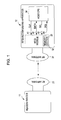
- Fig. 1 is a diagram showing a configuration of a system according to an embodiment of the present invention.
- the system shown in Fig. 1 includes a reader/writer 11 and an RFID-incorporated apparatus 12.
- RFID is an abbreviation of "Radio Frequency Identification”.
- RFID by using near-field wireless communication based on electromagnetic fields or radio waves, information is transmitted to and received from a tag embedded with ID information.
- the reader/writer 11 includes an RF antenna 21, and the RFID-incorporated apparatus 12 includes an RF antenna 31.
- the reader/writer 11 and the RFID-incorporated apparatus 12 communicate with each other by using the RF antenna 21 and the RF antenna 31.
- the RFID-incorporated apparatus 12 includes an RFID module 32 and a host CPU (Central Processing Unit) 34.
- the RFID module 32 controls communication with the reader/writer 11 through the RF antenna 31. Then, the RFID module 32 communicates with the host CPU 34.
- the RFID module 32 includes a memory section 33 such as a RAM (Random Access Memory), a register, or a nonvolatile memory. Then, the RFID module 32 temporarily stores data, transmitted from the reader/writer 11 or the host CPU 34, in the memory section 33.
- the RFID module 32 and the host CPU 34 are connected to each other by using wire communication configured to include four lines.
- the wire communication includes a CLK line 41 used for supplying a clock signal from the host CPU 34 to the RFID module 32 and an interactive DATA line 42 used for transmitting and receiving data between the RFID module 32 and the host CPU 34.
- the wire communication includes a SEL line 43 used for supplying, from the host CPU 34 to the RFID module 32, an instruction expressing the direction of data transfer and an IRQ line 44 used for supplying, from the RFID module 32 to the host CPU 34, an instruction expressing an interrupt.
- the RFID-incorporated apparatus 12 may include the RFID module 32 and the host CPU 34 as shown in Fig. 1
- the RFID module 32 and the host CPU 34 may be separately provided.
- the RFID module 32 and the host CPU 34 are connected to each other by using a predetermined interface, and the RFID module 32 is detachable from an apparatus including the host CPU 34.
- the apparatus including the host CPU 34 and having no function to communicate with the reader/writer 11, can communicate with the reader/writer 11 when the RFID module 32 is attached to the apparatus, for example. In this way, data stored in the apparatus including the host CPU 34 can be supplied to the reader/writer 11 when the RFID module 32 is attached as necessary, for example.
- the RFID-incorporated apparatus 12 including the RFID module 32 and the host CPU 34 as shown in Fig. 1 will be described as an example.
- the reader/writer 11 and the RFID-incorporated apparatus 12 communicate with each other by using wireless communication
- the RFID module 32 and the host CPU 34 communicate with each other by using wire communication.
- An example of communication will be described with reference to Fig. 2 .
- a process relating to communication will be briefly described with reference to Fig. 2 and, after that, be described in detail with reference to Figs. 4 to 7 .
- Step S11 data is transmitted from the host CPU 34 to the RFID module 32.
- the data is initial data. Fractional amounts of the data divided by a predetermined unit are transmitted more than once.
- Step S31 the RFID module 32 receives, more than once, data transmitted from the host CPU 34. The data is transmitted through the DATA line 42. Then, the data transmission starts when the host CPU 34 is ready.
- Step S32 the RFID module 32 receives the notice of data-transmission completion from the host CPU 34. At this time, the RFID module 32 detects the rise of a SEL signal transmitted through the SEL line 43. In this way, data transmission from the host CPU 34 to the RFID module 32 is performed.
- Step S61 the reader/writer 11 sends a polling request.
- the reader/writer 11 detects an apparatus which is located near and capable of communicating, in this case, the RFID-incorporated apparatus 12, the reader/writer 11 starts communication with the detected apparatus.
- the RFID module 32 included in the RFID-incorporated apparatus 12 receives the polling request from the reader/writer 11 in Step S33 and sends a polling response in Step S34.
- the reader/writer 11 receives the polling response in Step S62 and sends a command request in Step S63.
- Step S35 the RFID module 32 receives the command request.
- the RFID module 32 When the RFID module 32 receives the command request, the RFID module 32 stores a necessary portion of the received command request in the memory section 33, the portion including "Length” and "DATA".
- the "Length” refers to the data length of the "DATA”
- the "DATA” refers to the main part of the data.
- Step S36 the RFID module 32 sends a notice of data reception to the host CPU 34 through the IRQ line 44. Namely, the RFID module 32 sends an interrupt signal to the host CPU 34.
- Step S37 when the host CPU 34 is ready, the RFID module 32 reads out the "Length” and the "DATA" from the memory section 33 in synchronization with the clock signal supplied by the host CPU through the CLK line 41. Then, the RFID module 32 transmits, more than once, fractional amounts of the data divided by a predetermined unit to the host CPU 34 through the DATA line 42.
- Step S14 the host CPU 34 receives the "Length” and the "DATA" transmitted more than once from the RFID module 32. Then, the transfer is terminated.
- a command request 71 includes data 72 indicating the "Length”, data 73 including a command code, data 74 including the "DATA" as the main part of the data, and data 75 including CRC (Cyclic Redundancy Checking).
- the command request 71 is transmitted and received between the reader/writer 11 and the RFID module 32.
- the RFID module 32 analyzes a data portion including the data 73, that is, a command code.
- a command code When, on the basis of an analysis result of the command code, it is determined that transmission of data 74 (DATA) to the host CPU 34 is necessary, the RFID module 32 transmits data as shown in Fig. 3B to the host CPU 34.
- the data 72 and the data 74 are transmitted from the RFID module 32 to the host CPU 34.
- the data 72, the "Length", indicating the data length of the data 74 is transmitted from the RFID module 32 to the host CPU 34.
- the data 74, the main part of the data is transmitted.
- the data transmitted from the reader/writer 11 is data including a command.
- the RFID module 32 analyzes the command included in the received data and transmits (transfers) the main part of the data to the host CPU 34 on the basis of the analysis result. Therefore, when, on the basis of the analysis result, it is determined that transmission of the main part of the data to the host CPU 34 is not necessary, the main part of the data is not transferred to the host CPU 34, as the case may be. In this way, since the host CPU 34 avoids the analysis of the command included in the command request transmitted from the reader/writer 11, a circuit or a program used for the analysis may be reduced in size.
- the host CPU 34 when the host CPU 34 sends, to the RFID module 32, a reply in response to a command response, the host CPU 34 switches the status of the SEL signal transmitted through the SEL line 43 from H (High) to L (Low) and switches the transfer direction of the DATA line 42 to a direction in which data is transferred from the host CPU 34 to the RFID module 32.
- Step S15 data is transmitted from the host CPU 34 to the RFID module 32.
- the host CPU 34 transmits data to the RFID module 32 through the DATA line 42, the transmission of data being more than once and in synchronization with the clock signal supplied by the host CPU through the CLK line 41.
- the RFID module 32 receives the data.
- the RFID module 32 stores the received data in the memory section 33 as necessary.
- Step S39 the RFID module 32 receives the notice of data-transmission completion from the host CPU 34. At this time, the RFID module 32 detects the rise of the SEL signal transmitted through the SEL line 43. In this way, data transmission from the host CPU 34 to the RFID module 32 is performed.
- Step S40 the RFID module 32 reads out the data stored in the memory section 33, adds necessary information to the data, and sends a command response (the read out data) to the reader/writer 11.
- Step S64 the reader/writer 11 receives the command response from the RFID module 32.
- the "DATA" which the host CPU 34 is scheduled to transmit to the RFID module 32 corresponds to data 81.
- Content which the host CPU 34 is scheduled to transmit to the reader/writer 11 as a command response is described in the data 81.
- the RFID module 32 When the RFID module 32 receives the data 81, the RFID module 32 generates a command response 82 as shown in Fig. 3D and transmits the command response 82 to the reader/writer 11.
- the command request 82 includes data 83 indicating the "Length”, data 84 including a command code, data 81 including the "DATA” as the main part of the data, and data 85 including CRC (Cyclic Redundancy Checking).
- the RFID module 32 generates the command response 82 by adding, to the data 81, the data 83 corresponding to "Length", the data 84 including a command code, and the data 85 including CRC.
- the data 83 indicates the data length of the data 81, and the command code instructs the reader/writer 11 on the content of a process.
- the command response 82 is transmitted and received between the reader/writer 11 and the RFID module 32.
- the data 81 may include the "Length”. Namely, when the host CPU 34 supplies the data 81, the "Length" data included in the data 81 may be supplied to the RFID module 32. In this case, the "Length” data included in the data 81 may be extracted in the RFID module 32 and be supplied to the command response 82 as the data 83.
- the RFID module 32 adds a command code to the data 81 transmitted from the host CPU 34, the host CPU 34 does not recognize a command for the reader/writer 11. Therefore, a circuit or a program used for the recognition may be reduced in size.
- the communication between the reader/writer 11 and the RFID module 32 is performed by using wireless communication. Therefore, even though the communication channel is relatively unstable, data transmission and reception are correctly performed by adding the data 75 (the data 85) including CRC to data to transmit and receive. Compared with the wireless communication, the communication between the RFID module 32 and the host CPU 34 is performed by using wire communication. Therefore, since the communication channel is relatively stable, data transmission and reception are performed by adding no data including CRC. Even though data transmission and reception are accomplished during a relatively short period of time such as contact time in a system in which contactless communication is performed, data transmission and reception are robustly performed with the well-controlled communication mentioned above.
- the communication between the reader/writer 11 and the RFID-incorporated apparatus 12 is performed. Then, in this way, the communication between the RFID module 32 and the host CPU 34 is performed. In addition, the communication between the RFID module 32 and the host CPU 34 will be further described.
- four patterns may be applied to the communication between the RFID module 32 and the host CPU 34. Namely, in the first pattern, data transmission from the RFID module 32 to the host CPU 34 is performed and terminated. In the second pattern, data transmission from the host CPU 34 to the RFID module 32 is performed and terminated.
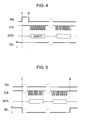
- the first pattern will be described with reference to Fig. 4 .
- the first pattern is a process related to the communication between the RFID module 32 and the host CPU 34, in which data transmission from the RFID module 32 to the host CPU 34 is performed and terminated. For example, the communication is performed when a command request from the reader/writer 11 is received.
- the RFID module 32 When the RFID module 32 receives, for example, a command request from the reader/writer 11 at timing t1, the RFID module 32 sends an IRQ signal to the host CPU 34 through the IRQ line 44. In this way, when the RFID module 32 is scheduled to supply data to the host CPU 34, the RFID module 32 sends the IRQ signal (an interrupt signal) to the host CPU 34 through the IRQ line 44.
- the host CPU 34 If the host CPU 34 receives the IRQ signal, the host CPU 34 supplies a clock signal to the RFID module 32 through the CLK line 41 when, at timing t2, the host CPU 34 is ready for receiving the data.
- the RFID module 32 receives the clock signal, the RFID module 32 transmits the data in synchronization with the clock signal.
- the first data which the RFID module 32 sends to the host CPU 34 is "Length” indicating the data length of data. After the “Length” is transferred, data such as a command from the reader/writer 11 is transferred. Therefore, the “Length” indicates the data length of data transferred (transmitted) after the "Length".
- the host CPU By receiving the "Length”, the host CPU recognizes the data length of the transferred data. Then, by recognizing the data length of the transferred data, the host CPU can determine whether or not data transfer is terminated. Namely, after receiving the "Length", the host CPU starts counting the data length of the transferred data (received data). Then, the host CPU detects the termination of data transfer when a count value corresponding to counted data length is equal to or greater than data length indicated by the "Length".
- an H (High) state of a signal communicated through the SEL line 43 is retained.
- the signal communicated through the SEL line 43 has two states, H (High) and L (Low).
- the H (High) state of the signal communicated through the SEL line 43 indicates a state in which data is transmitted from the RFID module 32 to the host CPU 34.
- the L (Low) state of the signal communicated through the SEL line 43 indicates a state in which data is transmitted from the host CPU 34 to the RFID module 32.
- the signal communicated through the SEL line 43 indicates the direction of data transmission. Then, the direction of data transmission in the communication between the RFID module 32 and the host CPU 34 is switched by switching the state of the signal communicated through the SEL line 43.
- the H (High) state of the signal communicated through the SEL line 43 data is transmitted from the RFID module 32 to the host CPU 34
- the L (Low) state of the signal communicated through the SEL line 43 data is transmitted from the host CPU 34 to the RFID module 32.
- descriptions, as below, relating to data communication are based on the above condition. Instead, an opposite condition may be set up. The opposite condition is that data is transmitted from the RFID module 32 to the host CPU 34 in the L (Low) state of the SEL line 43 and data is transmitted from the host CPU 34 to the RFID module 32 in the H (High) state of the SEL line 43.
- the host CPU 34 When the host CPU 34 is scheduled to transmit data to the RFID module 32 at timing t1, the host CPU 34 switches the state of the signal communicated through the SEL line 43 from H (high) to L (Low). Then, in this case, usually (in a standby state) the state of the SEL line 43 is set to the H (high) state. This is because the H (High) state means that data transmission from the RFID module 32 to the host CPU 34 can be performed and the host CPU 34 is maintained in a state in which an interrupt signal (IRQ signal) from the RFID module 32 can be received.
- IRQ signal interrupt signal
- the host CPU 34 switches the state of the signal communicated through the SEL line 43 from H (High) to L (Low) and the RFID module 32 detects the switching of the state. Accordingly, the RFID module 32 detects scheduled data transmission from the host CPU 34. Then, the RFID module 32 transits to a state in which data from the host CPU 34 can be received.
- the host CPU 34 When the host CPU 34 is ready after switching the state of the signal communicated through the SEL line 43 from H (High) to L (Low), the host CPU 34 transmits, to the RFID module 32, a clock signal through the CLK line 41 and data through the DATA line 42, the transmission of data being in synchronization with the clock signal.
- data When data is transmitted from the host CPU 34 to the RFID module 32, data itself is transmitted from the beginning and no data indicating data length such as the "Length" is transmitted. This is because the termination of data transmission from the host CPU 34 is not determined in the RFID module 32.
- the RFID module 32 detects the switching of the state. Accordingly, the RFID module 32 detects the termination of data transmission from the host CPU 34.
- the RFID module 32 does not transmit and receive a command which is transmitted and received in the communication of the related art, when data transmission is started or terminated. Accordingly, since a circuit or a program for generating or analyzing the command data may be unnecessary for the RFID module 32, the size of a circuit or memory size may be reduced. Therefore, reduction of power consumption may be realized.
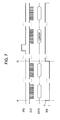
- communication in the third pattern will be described with reference to Fig. 6 .
- data transmission from the RFID module 32 to the host CPU 34 is performed, and, after that, data transmission from the host CPU 34 to the RFID module 32 is performed and terminated.
- the communication in the third pattern the communication in the first pattern and the communication in the second pattern are sequentially performed in this order.
- the communication in the third pattern is performed when a command request is received from the reader/writer 11 and a command response is sent in response to the command request.
- the RFID module 32 when the RFID module 32 receives the command request from the reader/writer 11 at timing t1, the RFID module 32 stores a necessary portion of the received command request in the memory section 33, the portion including "Length” and "DATA". Then, the RFID module 32 transmits an IRQ signal to the host CPU 34 through the IRQ line 44. If the host CPU 34 receives the IRQ signal, the host CPU 34 supplies a clock signal to the RFID module 32 through the CLK line 41 when, at timing t2, the host CPU 34 is ready for receiving data. When the RFID module 32 receives the clock signal, the RFID module 32 transmits data, such as the "Length" indicating data length, to the host CPU 34 in synchronization with the clock signal.
- the host CPU 34 When the host CPU 34 receives the "Length", the host CPU 34 recognizes the data length of transferred data and starts counting the data length of data transferred afterward (the data length of received data). Then, the host CPU detects the termination of data transfer when a count value corresponding to the counted data length is equal to data length indicated by the "Length". In response to the detection, the host CPU switches the state of a signal communicated through the SEL line 43 from H (High) to L (Low) at timing t3.
- the host CPU 34 transmits, to the RFID module 32, the clock signal through the CLK line 41 and data through the DATA line 42, the transmission of data being in synchronization with the clock signal.
- the host CPU 34 arranges a reply (data) in response to the command, transferred from the RFID module 32, of the reader/writer 11.
- the host CPU 34 transmits the reply through the DATA line 42 in synchronization with the clock signal.
- the host CPU 34 When the host CPU 34 terminates the data transmission at timing t4, the host CPU 34 returns the state of the signal communicated through the SEL line 43 from L (Low) to H (High). Accordingly, the RFID module 32 detects the termination of data transmission from the host CPU 34. After that, as necessary, the RFID module 32 adds necessary information to the data transmitted from the host CPU 34 and transmits a command response to the reader/writer 11.
- the host CPU 34 When the host CPU 34 is scheduled to transmit data to the RFID module 32 at timing t1, the host CPU 34 switches the state of a signal communicated through the SEL line 43 from H (high) to L (Low).
- the RFID module 32 detects the switching of the state of the signal communicated through the SEL line 43. Accordingly, the RFID module 32 detects scheduled data transmission from the host CPU 34. Then, the RFID module 32 transits to a state in which data from the host CPU 34 can be received.
- the host CPU 34 When the host CPU 34 is ready after switching the state of the signal communicated through the SEL line 43 from H (High) to L (Low), the host CPU 34 transmits, to the RFID module 32, a clock signal through the CLK line 41 and data through the DATA line 42, the transmission of data being in synchronization with the clock signal. When all data is transmitted, the host CPU 34 returns the state of the signal communicated through the SEL line 43 from L (Low) to H (High) at timing t2. Accordingly, the RFID module 32 detects the termination of data transmission from the host CPU 34.
- the RFID module 32 When the RFID module 32 transmits data to the host CPU 34 at a time point later than the timing t2, the RFID module 32 sends an IRQ signal to the host CPU 34 through the IRQ line 44. If the host CPU 34 receives the IRQ signal, the host CPU 34 supplies the clock signal to the RFID module 32 through the CLK line 41 when the host CPU 34 is ready for receiving data. When the RFID module 32 receives the clock signal, the RFID module 32 outputs data in synchronization with the clock signal.
- the RFID module 32 transmits data, such as "Length” indicating the data length of data, to the host CPU 34. Then, The RFID module 32 transmits data scheduled to be transmitted. After receiving the "Length", the host CPU starts counting the data length of the transmitted data (received data). Then, the host CPU detects the termination of data transfer when a count value corresponding to the counted data length is equal to or greater than data length indicated by the "Length". After detecting the termination of data transfer, the host CPU detects stops supplying the clock signal to the RFID module 32.
- the RFID module 32 and the host CPU 34 avoid sending forth a command used for instructing the start and termination of communication. Therefore, data length may be reduced when a command data is omitted.
- the start of communication is detected, if the host CPU 34 receives the IRQ signal or if the host CPU 34 switches the state of the signal communicated through the SEL line 43 from H (High) to L (Low) and supplies the clock signal through the CLK line 41.
- the start of communication is not performed by transmission and reception of a command code, the omitted command data may result in reduction of data length.
- the termination of communication is detected, if the host CPU 34 determines the termination on the basis of the "Length" from the RFID module 32, the "Length” being data relating to data length, or if the host CPU 34 switches the state of the signal communicated through the SEL line 43 from L (Low) to H (High).
- the termination of communication is not performed by transmission and reception of a command code, the omitted command data may result in reduction of data length.
- a function for generating or analyzing the command code may be omitted. Accordingly, in the RFID module 32 and the host CPU 34, the size of a circuit or memory size may be reduced and reduction of power consumption may be realized.
- the above-mentioned communication may be realized with no interface including an added signal line.
- the interrupt signal (IRQ signal) is used as a substitute for a signal line used for starting data transmission
- the data-transmission-direction signal line (SEL line) is used as a substitute for a signal line used for terminating data transmission
- data length is appended to the leading portion of data transmitted from the RFID module 32 (Slave) to the host CPU 34 (Master).
- the configuration realizes the above-mentioned communication. Therefore, a command code and decoding circuit used for analyzing the command code may be omitted with no signal line added to an interface. Therefore, according to an embodiment of the present invention, it may be expected that transfer efficiency is increased by reducing the amount of data, circuit size is reduced by reducing an encoding circuit and a decoding circuit or memory size, and power consumption is reduced.
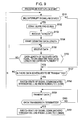
- Fig. 8 is a flowchart illustrating the process in the RFID module 32.
- Step S101 the RFID module 32 determines whether or not a command request is received from the reader/writer 11.
- a trigger starting data communication from the RFID module 32 to the host CPU 34 is reception of the command request from the reader/writer 11. Therefore, descriptions, as below, relating to the process is based on the above condition that, in Step S101, the RFID module 32 determines whether or not the command request is received from the reader/writer 11.
- the process in Step S101 is a process in which occurrence of such a trigger is determined.
- Step S101 the RFID module 32 determines that the command request is received from the reader/writer 11, the process proceeds to Step S102.
- Step S102 the received polling command is analyzed, and "Length" and "DATA" as an analysis result are stored in the memory section 33 as necessary. Namely, as described with reference to Fig. 3 , the command request 71 including the data 72 to the data 75 is received and a command code included in the data 73 is analyzed. Then, in response to the analysis result, the "Length" included in the data 72 and the "DATA" included in the data 74 are stored in the memory section 33.
- the RFID module 32 While the RFID module 32 does not analyze a command in communication between the RFID module 32 and the host CPU 34, the RFID module 32 analyzes a command from the reader/writer 11 in communication between the RFID module 32 and the reader/writer 11. The RFID module 32 analyzes the command from the reader/writer 11 and, in response to the analysis result, the RFID module 32 may perform communication between the RFID module 32 and the host CPU 34.
- the RFID module 32 may simply transfer the command from the reader/writer 11 to the host CPU 34 while the RFID module 32 does not analyze the command from the reader/writer 11.
- Step S103 the RFID module 32 outputs an IRQ signal (an interrupt signal) to the host CPU 34 through the IRQ line 44. Then, when the host CPU 34 starts supplying a clock signal through the CLK line 41 in response to the interrupt signal, the RFID module 32 outputs the "Length” in Step S104. For example, the RFID module 32 supplies the data length of a command as the "Length" to the host CPU 34, the data length being stored in the memory section 33.
- Step S105 the RFID module 32 transmits data, which is to be supplied to the host CPU 34, through the DATA line 42, the data being in synchronization with the supplied clock signal. Namely, data including the data 72 and the data 74 as shown in Fig. 3B is transmitted from the RFID module 32 to the host CPU 34. Since the RFID module 32 transmits data with no determination of whether or not data transmission is terminated, the RFID module 32 may proceed to a next process after data transmission is terminated.
- Step S101 After the data transmission is terminated or when, in Step S101, it is determined that no command request is received, the process proceeds to Step S106.
- the process from Step S101 through Step S105 as described above is a process in which the first patter is realized.
- Step S106 the RFID module 32 determines whether or not it is detected that the state of the signal communicated through the SEL line 43 is switched from H (High) to L (Low).
- Step S106 the RFID module 32 determines that it is not detected that the state of the signal communicated through the SEL line 43 is switched from H (High) to L (Low)
- the process returns to Step S101 and the following process is repeated.
- Step S106 the RFID module 32 determines that it is detected that the state of the signal communicated through the SEL line 43 is switched from H (High) to L (Low)
- the process proceeds to Step S107.
- Step S107 data transmitted from the host CPU 34 in synchronization with the clock signal (for example, the data 81 shown in Fig. 3C ) is received and stored in the memory section 33 as necessary.
- Step S108 the RFID module 32 determines whether or not it is detected that the state of the signal communicated through the SEL line 43 is switched from L (Low) to H (High).
- Step S108 the RFID module 32 determines that it is not detected that the state of the signal communicated through the SEL line 43 is switched from L (Low) to H (High), that is, when the host CPU 34 are transmitting data, the process returns to Step S107 and reception and storing of data are continued.
- Step S108 the RFID module 32 determines that it is detected that the state of the signal communicated through the SEL line 43 is switched from L (Low) to H (High), the process proceeds to Step S109.
- the RFID module 32 adds necessary information to the data stored in the memory section 33 and transmits the data to the reader/writer 11. Namely, as shown in Fig. 3D , the data 83 (the "Length"), the data 84 (a command code), and the data 85 (CRC) are appended to the data 81 transmitted from the host CPU 34, and the command response 82 is generated and transmitted to the reader/writer 11.
- Step S106 through Step S109 is a process in which the above-mentioned second patter is realized.
- the process in which Steps S101 to S109 are performed is a process in which the above-mentioned third patter is performed.
- the process in which Steps S106 to S109 are performed and, after that, Steps S101 to S105 are performed is a process in which the above-mentioned fourth patter is performed.
- the host CPU 32 sets the state of a signal communicated through the SEL line 43 to L (Low).
- Step S151 the host CPU 34 determines whether or not an IRQ signal (an interrupt signal) is received from the RFID module 32 through the IRQ line 44.
- an IRQ signal an interrupt signal
- the process proceeds to Step S152.
- the process proceeds to Step S157.
- Step S152 the host CPU 34 starts supplying a clock signal through the CLK line 41 when the host CPU 34 is ready for receiving data transmitted from the RFID module 32. If the clock signal is supplied to the RFID module 32, data corresponding to "Length", which is transmitted from the RFID module 32, is received in Step S153 in response to the clock signal. When the data corresponding to the "Length" is received, in Step S154 the host CPU starts counting the data length of the received data.
- Step S155 data transmitted from the RFID module 32 through the DATA line 42 is received. Every time the data is received, the data length of the received data is counted. Then, in Step S156, the host CPU determines whether or not the data length of the received data, that is, the counted data length is equal to or greater than data length indicated by the "Length".
- Step S156 the counted data length is determined to be smaller than data length indicated by the "Length", that is, the RFID module 32 is transmitting data, the process returns to S155 and data reception is continued.
- Step S156 the counted data length is determined to be equal to or greater than data length indicated by the "Length", that is, data transmission from the RFID module 32 is terminated, the process proceeds to S157.
- Step S151 through Step S156 is a process in which the above-mentioned first patter is realized.
- Step S157 the host CPU 34 determined whether or not data is scheduled to be transmitted to the RFID module 32.
- Step S157 it is determined that data is scheduled to be transmitted to the RFID module 32, the process proceeds to Step S158.
- Step S158 the process returns to Step S151 and the following process is repeated.
- Step S158 the host CPU 34 switches the state of the signal communicated through the SEL line 43 from H (high) to L (Low) so as to notify the RFID module 32 that data is scheduled to be transmitted. In this way, the state of the signal communicated through the SEL line 43 being switched, the state that the RFID module 32 can receive data is set. In addition to the state, when the host CPU 34 is ready for transmitting data, the process proceeds to Step S159.
- Step S159 the host CPU 34 transmits data to the RFID module 32 through the DATA line 42.
- the clock signal is not supplied to the RFID module 32 through the CLK line 41, supply of the clock signal starts before data transmission is performed.
- Step S160 the host CPU 34 determines whether or not data transmission is terminated. When data transmission is not determined to be terminated, the process returns to Step S159 and data transmission to the RFID module 32 is continued. On the other hand, when in Step S160 data transmission is determined to be terminated, the process proceeds to Step S161.
- Step S161 the host CPU 34 returns the state of the signal communicated through the SEL line 43 from L (Low) to H (High). In this way, the state of the signal communicated through the SEL line 43 being switched, the RFID module 32 detects the termination of data transmission and proceeds to a following process.
- Step S157 through Step S161 is a process in which the above-mentioned second patter is realized.
- the process in which Steps S151 to S161 are performed is a process in which the above-mentioned third patter is performed.
- the process in which Steps S157 to S161 are performed and, after that, Steps S151 to S156 are performed is a process in which the above-mentioned fourth patter is performed.
- a function for generating or analyzing the command may be unnecessary and the size of a circuit or memory size may be reduced. Furthermore, since such a function may be unnecessary in communication between the RFID module and the host CPU 34, no processing load may be necessary for analyzing the command. Therefore, overall processing load may be reduced and, as a result, power consumption may be reduced.
- the above-mentioned series of process may be performed with hardware or software.
- a program including the software is installed to a computer.
- the computer represents a computer embedded in a dedicated hardware and a computer, such as a universal personal computer, capable of executing various kinds of functions by installing various kinds of programs.
- Fig. 10 is a block diagram illustrating a hardware configuration example of a computer performing the above-mentioned series of process with a program.
- a CPU 101 In the computer, a CPU 101, a ROM (Read Only Memory) 102, and a RAM (Random Access Memory) 103 are connected with one another through a bus 104. Furthermore, an input-output interface 105 is connected to the bus 104. An input section 106, an output section 107, a memory section 108, a communication section 109, and a drive section 110 are connected to the input-output interface 105.
- the input section 106 includes a keyboard, a mouse, and a microphone.
- the output section 107 includes a display and a speaker.
- the memory section 108 includes a hard disk drive and a nonvolatile memory.
- the communication section 109 includes a network interface.
- the drive section 110 drives a removable medium 111 such as a magnetic disk, an optical disk, a magnet-optical disk, and a semiconductor memory.
- the CPU 101 loads a program, for example, stored in the memory section 108 into the RAM 103 through the input-output interface 105 and the bus 104 and performs the above-mentioned series of process.
- a program executed by the computer may be recorded in the removable medium 111 as a package medium and be provided.
- the program may be provided through a wire or wireless transmission medium such as local area network, internet, or Digital Satellite Broadcasting.
- the program may be installed to the memory section 108 through the input-output interface 105.
- the program may be received through a wire or wireless transmission medium and installed to the memory section 108.
- the program may be installed to the ROM 102 or the memory section 108 in advance.
- the program executed by the computer may be a program processed in temporal sequence along the order described in the specification, a program processed in parallel, or a program processed at necessary timing when a program call is executed.
- a system represents a whole apparatus including a plurality of apparatuses.
Landscapes
- Engineering & Computer Science (AREA)
- Theoretical Computer Science (AREA)
- Physics & Mathematics (AREA)
- General Engineering & Computer Science (AREA)
- General Physics & Mathematics (AREA)
- Signal Processing (AREA)
- Computer Networks & Wireless Communication (AREA)
- Information Transfer Systems (AREA)
- Mobile Radio Communication Systems (AREA)
- Communication Control (AREA)
- Near-Field Transmission Systems (AREA)
- Computer And Data Communications (AREA)
- Bus Control (AREA)
- Selective Calling Equipment (AREA)
Applications Claiming Priority (1)
| Application Number | Priority Date | Filing Date | Title |
|---|---|---|---|
| JP2008309577A JP5217982B2 (ja) | 2008-12-04 | 2008-12-04 | 情報処理装置および方法、並びにプログラム |
Publications (3)
| Publication Number | Publication Date |
|---|---|
| EP2194460A2 true EP2194460A2 (fr) | 2010-06-09 |
| EP2194460A3 EP2194460A3 (fr) | 2010-10-20 |
| EP2194460B1 EP2194460B1 (fr) | 2012-07-25 |
Family
ID=42122945
Family Applications (1)
| Application Number | Title | Priority Date | Filing Date |
|---|---|---|---|
| EP09177809A Not-in-force EP2194460B1 (fr) | 2008-12-04 | 2009-12-03 | Appareil de traitement d'informations, procédé et programme de traitement d'informations |
Country Status (4)
| Country | Link |
|---|---|
| US (2) | US8918556B2 (fr) |
| EP (1) | EP2194460B1 (fr) |
| JP (1) | JP5217982B2 (fr) |
| CN (2) | CN102902649B (fr) |
Cited By (3)
| Publication number | Priority date | Publication date | Assignee | Title |
|---|---|---|---|---|
| EP2693368A4 (fr) * | 2011-03-31 | 2014-06-11 | Panasonic Corp | Dispositif rfid, dispositif hôte, appareil sur lequel est monté un dispositif rfid et procédé de commande d'un dispositif rfid |
| CN106933762A (zh) * | 2015-09-30 | 2017-07-07 | 天工方案公司 | 内部串行接口 |
| CN113726498A (zh) * | 2020-10-26 | 2021-11-30 | 深圳市宏电技术股份有限公司 | 基于spi的双全工通信方法、主机、从机及存储介质 |
Families Citing this family (8)
| Publication number | Priority date | Publication date | Assignee | Title |
|---|---|---|---|---|
| JP4931912B2 (ja) * | 2006-04-26 | 2012-05-16 | パナソニック株式会社 | 信号伝送方法、送受信装置及び通信システム |
| WO2008035296A2 (fr) * | 2006-09-22 | 2008-03-27 | Koninklijke Philips Electronics N.V. | Fonctionnalité étendue de dispositifs d'identification par radiofréquence rfid |
| JP5217982B2 (ja) * | 2008-12-04 | 2013-06-19 | ソニー株式会社 | 情報処理装置および方法、並びにプログラム |
| KR101581853B1 (ko) * | 2010-12-23 | 2016-01-04 | 한국전자통신연구원 | 무선 주파수 인식 보안 리더 |
| JP5935235B2 (ja) | 2011-02-18 | 2016-06-15 | ソニー株式会社 | 通信装置、通信システムおよび通信方法 |
| JP2013140541A (ja) | 2012-01-06 | 2013-07-18 | Toshiba Corp | 半導体記憶装置 |
| JP6117562B2 (ja) * | 2013-02-13 | 2017-04-19 | ソニー株式会社 | 情報処理装置、情報処理方法および情報処理システム |
| EP2911066B1 (fr) * | 2014-02-19 | 2016-11-30 | Nxp B.V. | Procédé de transfert de données, dispositif de programme informatique et étiquette |
Citations (2)
| Publication number | Priority date | Publication date | Assignee | Title |
|---|---|---|---|---|
| JP2001290764A (ja) | 2000-04-06 | 2001-10-19 | Ricoh Co Ltd | データ転送システム装置及びそのデータ転送方法 |
| US20080143487A1 (en) | 2006-12-19 | 2008-06-19 | Broadcom Corporation | System and method for enabling interrupts for rfid tags |
Family Cites Families (29)
| Publication number | Priority date | Publication date | Assignee | Title |
|---|---|---|---|---|
| JPS6120182A (ja) * | 1984-07-06 | 1986-01-28 | Toshiba Corp | デ−タ処理システム |
| GB2173326B (en) * | 1985-03-18 | 1989-06-21 | Nitsuko Ltd | Data transmission system |
| JPH03278157A (ja) * | 1990-03-27 | 1991-12-09 | Seiko Epson Corp | 情報処理装置 |
| JP2650001B2 (ja) * | 1991-10-18 | 1997-09-03 | 富士通株式会社 | シリアル転送受信完了判別方式 |
| JP3451628B2 (ja) * | 1992-03-24 | 2003-09-29 | ソニー株式会社 | 4線式同期シリアル通信方式 |
| TW234228B (fr) * | 1992-05-28 | 1994-11-11 | Motorola Inc | |
| JP3315684B2 (ja) * | 1999-08-02 | 2002-08-19 | セコム株式会社 | 画像監視装置 |
| US6728908B1 (en) * | 1999-11-18 | 2004-04-27 | California Institute Of Technology | I2C bus protocol controller with fault tolerance |
| JP2002247157A (ja) * | 2001-02-15 | 2002-08-30 | Toppan Forms Co Ltd | 携帯電話機及び携帯電話機に用いられるタグ、並びに該携帯電話機の使用方法 |
| US6799233B1 (en) * | 2001-06-29 | 2004-09-28 | Koninklijke Philips Electronics N.V. | Generalized I2C slave transmitter/receiver state machine |
| JP4006274B2 (ja) * | 2002-06-25 | 2007-11-14 | 株式会社リコー | 記録方法、プログラム及び記録媒体、情報処理装置、情報記録装置、並びに情報記録システム |
| JP2004005842A (ja) * | 2002-05-31 | 2004-01-08 | Ricoh Co Ltd | 記録方法、記録媒体、プログラム及び情報記録媒体、並びに情報記録装置 |
| JP2005084791A (ja) * | 2003-09-05 | 2005-03-31 | Alpine Electronics Inc | データ通信方法 |
| JP4539071B2 (ja) * | 2003-10-23 | 2010-09-08 | ソニー株式会社 | 携帯無線通信装置。 |
| KR20050076924A (ko) * | 2004-01-26 | 2005-07-29 | 삼성전자주식회사 | 양방향 통신이 가능한 i2c 통신시스템 및 그 방법 |
| JP3809839B2 (ja) * | 2004-03-09 | 2006-08-16 | セイコーエプソン株式会社 | データ転送制御装置、電子機器及びデータ転送制御方法 |
| JP2006119693A (ja) * | 2004-10-19 | 2006-05-11 | Sony Corp | 情報処理装置及び情報処理方法、並びにコンピュータ・プログラム |
| US7769963B1 (en) * | 2005-02-09 | 2010-08-03 | Tc License Ltd. | RF tag system with single step read and write commands |
| US7604178B2 (en) * | 2005-05-11 | 2009-10-20 | Intelleflex Corporation | Smart tag activation |
| US8248211B2 (en) * | 2005-07-20 | 2012-08-21 | Intelleflex Corporation | Selective RF device activation |
| DE102006004346A1 (de) * | 2006-01-30 | 2007-10-18 | Deutsche Thomson-Brandt Gmbh | Datenbusschnittstelle mit abschaltbarem Takt |
| US8508369B2 (en) * | 2006-09-01 | 2013-08-13 | Intermec Ip Corp. | RFID tag system with block coding, such as space-time block coding |
| JP2008186350A (ja) * | 2007-01-31 | 2008-08-14 | Kyocera Mita Corp | 通信システム及び画像形成装置 |
| JP2008270978A (ja) * | 2007-04-17 | 2008-11-06 | Toshiba Tec Corp | 無線通信装置 |
| JP5355936B2 (ja) * | 2007-06-28 | 2013-11-27 | 日本信号株式会社 | リーダライタ、及び物品仕分システム |
| US20090033493A1 (en) * | 2007-07-31 | 2009-02-05 | Symbol Technologies, Inc. | Method, System and Apparatus for Writing Common Information to a Plurality of Radio Frequency Identification (RFID) Tags |
| EP2179364B1 (fr) * | 2007-08-15 | 2011-01-12 | Nxp B.V. | Interface de bus i 2 c à mode opératoire parallèle |
| US20090259786A1 (en) * | 2008-04-10 | 2009-10-15 | Chu-Ming Lin | Data transfer system and method for host-slave interface with automatic status report |
| JP5217982B2 (ja) * | 2008-12-04 | 2013-06-19 | ソニー株式会社 | 情報処理装置および方法、並びにプログラム |
-
2008
- 2008-12-04 JP JP2008309577A patent/JP5217982B2/ja not_active Expired - Fee Related
-
2009
- 2009-11-04 US US12/590,232 patent/US8918556B2/en not_active Expired - Fee Related
- 2009-12-03 EP EP09177809A patent/EP2194460B1/fr not_active Not-in-force
- 2009-12-04 CN CN201210165889.XA patent/CN102902649B/zh not_active Expired - Fee Related
- 2009-12-04 CN CN2009102531818A patent/CN101751587B/zh not_active Expired - Fee Related
-
2014
- 2014-11-24 US US14/551,559 patent/US9864723B2/en not_active Expired - Fee Related
Patent Citations (2)
| Publication number | Priority date | Publication date | Assignee | Title |
|---|---|---|---|---|
| JP2001290764A (ja) | 2000-04-06 | 2001-10-19 | Ricoh Co Ltd | データ転送システム装置及びそのデータ転送方法 |
| US20080143487A1 (en) | 2006-12-19 | 2008-06-19 | Broadcom Corporation | System and method for enabling interrupts for rfid tags |
Cited By (4)
| Publication number | Priority date | Publication date | Assignee | Title |
|---|---|---|---|---|
| EP2693368A4 (fr) * | 2011-03-31 | 2014-06-11 | Panasonic Corp | Dispositif rfid, dispositif hôte, appareil sur lequel est monté un dispositif rfid et procédé de commande d'un dispositif rfid |
| US9141904B2 (en) | 2011-03-31 | 2015-09-22 | Panasonic Intellectual Property Corporation Of America | RFID device, host, RFID-embedded apparatus, and method of controlling RFID device |
| CN106933762A (zh) * | 2015-09-30 | 2017-07-07 | 天工方案公司 | 内部串行接口 |
| CN113726498A (zh) * | 2020-10-26 | 2021-11-30 | 深圳市宏电技术股份有限公司 | 基于spi的双全工通信方法、主机、从机及存储介质 |
Also Published As
| Publication number | Publication date |
|---|---|
| US8918556B2 (en) | 2014-12-23 |
| EP2194460B1 (fr) | 2012-07-25 |
| CN101751587A (zh) | 2010-06-23 |
| CN102902649A (zh) | 2013-01-30 |
| JP2010134672A (ja) | 2010-06-17 |
| JP5217982B2 (ja) | 2013-06-19 |
| EP2194460A3 (fr) | 2010-10-20 |
| US9864723B2 (en) | 2018-01-09 |
| CN101751587B (zh) | 2012-12-26 |
| US20100141387A1 (en) | 2010-06-10 |
| US20150081939A1 (en) | 2015-03-19 |
| CN102902649B (zh) | 2017-11-03 |
Similar Documents
| Publication | Publication Date | Title |
|---|---|---|
| EP2194460B1 (fr) | Appareil de traitement d'informations, procédé et programme de traitement d'informations | |
| KR100912076B1 (ko) | 리더/태그 통합형 rfid 장치 및 방법 | |
| EP2124155B1 (fr) | Appareil de traitement d'informations, système de traitement d'informations, procédé de traitement d'informations, et programme informatique | |
| US20100088454A1 (en) | Bridging device with power-saving function | |
| EP3293887B1 (fr) | Dispositif de communication de champ proche | |
| CN101404057A (zh) | 减小rfid交换中的处理等待时间 | |
| US9703996B2 (en) | Method for managing communication between an electronic device, for example a contactless chip card, and a communication apparatus, for example a reader, and corresponding electronic device | |
| JP7434413B2 (ja) | 電子機器、および制御方法 | |
| US9007176B2 (en) | Portable electronic apparatus and control method of portable electronic apparatus | |
| EP2163968A2 (fr) | Puce CI, dispositif de traitement d'informations, système de traitement des informations et programmes | |
| CN112613329A (zh) | 用于电路之间的通信的方法 | |
| EP2360626A1 (fr) | Dispositif électronique portable et procédé de contrôle d'un dispositif électronique portable | |
| KR100736405B1 (ko) | Fifo없이 dma를 수행할 수 있는 반도체 장치와 상기반도체 장치의 데이터 처리방법 | |
| JP4803017B2 (ja) | 通信処理装置、通信処理方法、およびプログラム | |
| KR100848350B1 (ko) | 모드 상태에 따라 전원 공급을 제어하기 위한 rfid장치 | |
| EP1895426A1 (fr) | Émetteur et système de transmission qui l'utilise | |
| EP1983443A1 (fr) | Procédé de communication en série et système de communication en série | |
| WO2025141509A1 (fr) | Cœur numérique d'étiquette rfid, interprétateur de démodulation rfid et circuit de préparation et de mise en forme de réponse rfid | |
| CN111756390A (zh) | 一种多通道射频读写装置 | |
| KR20180028872A (ko) | 근거리 무선 통신 장치 |
Legal Events
| Date | Code | Title | Description |
|---|---|---|---|
| PUAI | Public reference made under article 153(3) epc to a published international application that has entered the european phase |
Free format text: ORIGINAL CODE: 0009012 |
|
| 17P | Request for examination filed |
Effective date: 20091203 |
|
| AK | Designated contracting states |
Kind code of ref document: A2 Designated state(s): AT BE BG CH CY CZ DE DK EE ES FI FR GB GR HR HU IE IS IT LI LT LU LV MC MK MT NL NO PL PT RO SE SI SK SM TR |
|
| PUAL | Search report despatched |
Free format text: ORIGINAL CODE: 0009013 |
|
| AK | Designated contracting states |
Kind code of ref document: A3 Designated state(s): AT BE BG CH CY CZ DE DK EE ES FI FR GB GR HR HU IE IS IT LI LT LU LV MC MK MT NL NO PL PT RO SE SI SK SM TR |
|
| RIC1 | Information provided on ipc code assigned before grant |
Ipc: G06F 13/32 20060101AFI20100504BHEP Ipc: H04B 5/02 20060101ALI20100914BHEP |
|
| GRAP | Despatch of communication of intention to grant a patent |
Free format text: ORIGINAL CODE: EPIDOSNIGR1 |
|
| GRAS | Grant fee paid |
Free format text: ORIGINAL CODE: EPIDOSNIGR3 |
|
| GRAA | (expected) grant |
Free format text: ORIGINAL CODE: 0009210 |
|
| AK | Designated contracting states |
Kind code of ref document: B1 Designated state(s): AT BE BG CH CY CZ DE DK EE ES FI FR GB GR HR HU IE IS IT LI LT LU LV MC MK MT NL NO PL PT RO SE SI SK SM TR |
|
| REG | Reference to a national code |
Ref country code: GB Ref legal event code: FG4D |
|
| REG | Reference to a national code |
Ref country code: CH Ref legal event code: EP |
|
| REG | Reference to a national code |
Ref country code: AT Ref legal event code: REF Ref document number: 567956 Country of ref document: AT Kind code of ref document: T Effective date: 20120815 Ref country code: IE Ref legal event code: FG4D |
|
| REG | Reference to a national code |
Ref country code: DE Ref legal event code: R096 Ref document number: 602009008463 Country of ref document: DE Effective date: 20120920 |
|
| REG | Reference to a national code |
Ref country code: NL Ref legal event code: VDEP Effective date: 20120725 |
|
| REG | Reference to a national code |
Ref country code: AT Ref legal event code: MK05 Ref document number: 567956 Country of ref document: AT Kind code of ref document: T Effective date: 20120725 |
|
| REG | Reference to a national code |
Ref country code: LT Ref legal event code: MG4D Effective date: 20120725 |
|
| PG25 | Lapsed in a contracting state [announced via postgrant information from national office to epo] |
Ref country code: HR Free format text: LAPSE BECAUSE OF FAILURE TO SUBMIT A TRANSLATION OF THE DESCRIPTION OR TO PAY THE FEE WITHIN THE PRESCRIBED TIME-LIMIT Effective date: 20120725 Ref country code: AT Free format text: LAPSE BECAUSE OF FAILURE TO SUBMIT A TRANSLATION OF THE DESCRIPTION OR TO PAY THE FEE WITHIN THE PRESCRIBED TIME-LIMIT Effective date: 20120725 Ref country code: LT Free format text: LAPSE BECAUSE OF FAILURE TO SUBMIT A TRANSLATION OF THE DESCRIPTION OR TO PAY THE FEE WITHIN THE PRESCRIBED TIME-LIMIT Effective date: 20120725 Ref country code: CY Free format text: LAPSE BECAUSE OF FAILURE TO SUBMIT A TRANSLATION OF THE DESCRIPTION OR TO PAY THE FEE WITHIN THE PRESCRIBED TIME-LIMIT Effective date: 20120725 Ref country code: FI Free format text: LAPSE BECAUSE OF FAILURE TO SUBMIT A TRANSLATION OF THE DESCRIPTION OR TO PAY THE FEE WITHIN THE PRESCRIBED TIME-LIMIT Effective date: 20120725 Ref country code: NO Free format text: LAPSE BECAUSE OF FAILURE TO SUBMIT A TRANSLATION OF THE DESCRIPTION OR TO PAY THE FEE WITHIN THE PRESCRIBED TIME-LIMIT Effective date: 20121025 Ref country code: BE Free format text: LAPSE BECAUSE OF FAILURE TO SUBMIT A TRANSLATION OF THE DESCRIPTION OR TO PAY THE FEE WITHIN THE PRESCRIBED TIME-LIMIT Effective date: 20120725 Ref country code: IS Free format text: LAPSE BECAUSE OF FAILURE TO SUBMIT A TRANSLATION OF THE DESCRIPTION OR TO PAY THE FEE WITHIN THE PRESCRIBED TIME-LIMIT Effective date: 20121125 |
|
| PG25 | Lapsed in a contracting state [announced via postgrant information from national office to epo] |
Ref country code: GR Free format text: LAPSE BECAUSE OF FAILURE TO SUBMIT A TRANSLATION OF THE DESCRIPTION OR TO PAY THE FEE WITHIN THE PRESCRIBED TIME-LIMIT Effective date: 20121026 Ref country code: SI Free format text: LAPSE BECAUSE OF FAILURE TO SUBMIT A TRANSLATION OF THE DESCRIPTION OR TO PAY THE FEE WITHIN THE PRESCRIBED TIME-LIMIT Effective date: 20120725 Ref country code: LV Free format text: LAPSE BECAUSE OF FAILURE TO SUBMIT A TRANSLATION OF THE DESCRIPTION OR TO PAY THE FEE WITHIN THE PRESCRIBED TIME-LIMIT Effective date: 20120725 Ref country code: PT Free format text: LAPSE BECAUSE OF FAILURE TO SUBMIT A TRANSLATION OF THE DESCRIPTION OR TO PAY THE FEE WITHIN THE PRESCRIBED TIME-LIMIT Effective date: 20121126 Ref country code: PL Free format text: LAPSE BECAUSE OF FAILURE TO SUBMIT A TRANSLATION OF THE DESCRIPTION OR TO PAY THE FEE WITHIN THE PRESCRIBED TIME-LIMIT Effective date: 20120725 Ref country code: SE Free format text: LAPSE BECAUSE OF FAILURE TO SUBMIT A TRANSLATION OF THE DESCRIPTION OR TO PAY THE FEE WITHIN THE PRESCRIBED TIME-LIMIT Effective date: 20120725 |
|
| PG25 | Lapsed in a contracting state [announced via postgrant information from national office to epo] |
Ref country code: NL Free format text: LAPSE BECAUSE OF FAILURE TO SUBMIT A TRANSLATION OF THE DESCRIPTION OR TO PAY THE FEE WITHIN THE PRESCRIBED TIME-LIMIT Effective date: 20120725 |
|
| PG25 | Lapsed in a contracting state [announced via postgrant information from national office to epo] |
Ref country code: CZ Free format text: LAPSE BECAUSE OF FAILURE TO SUBMIT A TRANSLATION OF THE DESCRIPTION OR TO PAY THE FEE WITHIN THE PRESCRIBED TIME-LIMIT Effective date: 20120725 Ref country code: RO Free format text: LAPSE BECAUSE OF FAILURE TO SUBMIT A TRANSLATION OF THE DESCRIPTION OR TO PAY THE FEE WITHIN THE PRESCRIBED TIME-LIMIT Effective date: 20120725 Ref country code: EE Free format text: LAPSE BECAUSE OF FAILURE TO SUBMIT A TRANSLATION OF THE DESCRIPTION OR TO PAY THE FEE WITHIN THE PRESCRIBED TIME-LIMIT Effective date: 20120725 Ref country code: DK Free format text: LAPSE BECAUSE OF FAILURE TO SUBMIT A TRANSLATION OF THE DESCRIPTION OR TO PAY THE FEE WITHIN THE PRESCRIBED TIME-LIMIT Effective date: 20120725 Ref country code: ES Free format text: LAPSE BECAUSE OF FAILURE TO SUBMIT A TRANSLATION OF THE DESCRIPTION OR TO PAY THE FEE WITHIN THE PRESCRIBED TIME-LIMIT Effective date: 20121105 |
|
| PG25 | Lapsed in a contracting state [announced via postgrant information from national office to epo] |
Ref country code: IT Free format text: LAPSE BECAUSE OF FAILURE TO SUBMIT A TRANSLATION OF THE DESCRIPTION OR TO PAY THE FEE WITHIN THE PRESCRIBED TIME-LIMIT Effective date: 20120725 Ref country code: SK Free format text: LAPSE BECAUSE OF FAILURE TO SUBMIT A TRANSLATION OF THE DESCRIPTION OR TO PAY THE FEE WITHIN THE PRESCRIBED TIME-LIMIT Effective date: 20120725 |
|
| PLBE | No opposition filed within time limit |
Free format text: ORIGINAL CODE: 0009261 |
|
| STAA | Information on the status of an ep patent application or granted ep patent |
Free format text: STATUS: NO OPPOSITION FILED WITHIN TIME LIMIT |
|
| 26N | No opposition filed |
Effective date: 20130426 |
|
| PG25 | Lapsed in a contracting state [announced via postgrant information from national office to epo] |
Ref country code: MC Free format text: LAPSE BECAUSE OF NON-PAYMENT OF DUE FEES Effective date: 20121231 Ref country code: BG Free format text: LAPSE BECAUSE OF FAILURE TO SUBMIT A TRANSLATION OF THE DESCRIPTION OR TO PAY THE FEE WITHIN THE PRESCRIBED TIME-LIMIT Effective date: 20121025 |
|
| REG | Reference to a national code |
Ref country code: DE Ref legal event code: R097 Ref document number: 602009008463 Country of ref document: DE Effective date: 20130426 |
|
| REG | Reference to a national code |
Ref country code: IE Ref legal event code: MM4A |
|
| PG25 | Lapsed in a contracting state [announced via postgrant information from national office to epo] |
Ref country code: IE Free format text: LAPSE BECAUSE OF NON-PAYMENT OF DUE FEES Effective date: 20121203 |
|
| PG25 | Lapsed in a contracting state [announced via postgrant information from national office to epo] |
Ref country code: MT Free format text: LAPSE BECAUSE OF FAILURE TO SUBMIT A TRANSLATION OF THE DESCRIPTION OR TO PAY THE FEE WITHIN THE PRESCRIBED TIME-LIMIT Effective date: 20120725 |
|
| PG25 | Lapsed in a contracting state [announced via postgrant information from national office to epo] |
Ref country code: TR Free format text: LAPSE BECAUSE OF FAILURE TO SUBMIT A TRANSLATION OF THE DESCRIPTION OR TO PAY THE FEE WITHIN THE PRESCRIBED TIME-LIMIT Effective date: 20120725 |
|
| PG25 | Lapsed in a contracting state [announced via postgrant information from national office to epo] |
Ref country code: SM Free format text: LAPSE BECAUSE OF FAILURE TO SUBMIT A TRANSLATION OF THE DESCRIPTION OR TO PAY THE FEE WITHIN THE PRESCRIBED TIME-LIMIT Effective date: 20120725 Ref country code: LU Free format text: LAPSE BECAUSE OF NON-PAYMENT OF DUE FEES Effective date: 20121203 |
|
| PG25 | Lapsed in a contracting state [announced via postgrant information from national office to epo] |
Ref country code: HU Free format text: LAPSE BECAUSE OF FAILURE TO SUBMIT A TRANSLATION OF THE DESCRIPTION OR TO PAY THE FEE WITHIN THE PRESCRIBED TIME-LIMIT Effective date: 20091203 |
|
| REG | Reference to a national code |
Ref country code: CH Ref legal event code: PL |
|
| PG25 | Lapsed in a contracting state [announced via postgrant information from national office to epo] |
Ref country code: LI Free format text: LAPSE BECAUSE OF NON-PAYMENT OF DUE FEES Effective date: 20131231 Ref country code: CH Free format text: LAPSE BECAUSE OF NON-PAYMENT OF DUE FEES Effective date: 20131231 |
|
| REG | Reference to a national code |
Ref country code: DE Ref legal event code: R084 Ref document number: 602009008463 Country of ref document: DE |
|
| REG | Reference to a national code |
Ref country code: GB Ref legal event code: 746 Effective date: 20150421 |
|
| REG | Reference to a national code |
Ref country code: DE Ref legal event code: R084 Ref document number: 602009008463 Country of ref document: DE Effective date: 20150410 |
|
| PG25 | Lapsed in a contracting state [announced via postgrant information from national office to epo] |
Ref country code: MK Free format text: LAPSE BECAUSE OF FAILURE TO SUBMIT A TRANSLATION OF THE DESCRIPTION OR TO PAY THE FEE WITHIN THE PRESCRIBED TIME-LIMIT Effective date: 20120725 |
|
| REG | Reference to a national code |
Ref country code: FR Ref legal event code: PLFP Year of fee payment: 7 |
|
| REG | Reference to a national code |
Ref country code: FR Ref legal event code: PLFP Year of fee payment: 8 |
|
| REG | Reference to a national code |
Ref country code: FR Ref legal event code: PLFP Year of fee payment: 9 |
|
| PGFP | Annual fee paid to national office [announced via postgrant information from national office to epo] |
Ref country code: DE Payment date: 20211117 Year of fee payment: 13 Ref country code: GB Payment date: 20211118 Year of fee payment: 13 Ref country code: FR Payment date: 20211117 Year of fee payment: 13 |
|
| REG | Reference to a national code |
Ref country code: DE Ref legal event code: R119 Ref document number: 602009008463 Country of ref document: DE |
|
| GBPC | Gb: european patent ceased through non-payment of renewal fee |
Effective date: 20221203 |
|
| PG25 | Lapsed in a contracting state [announced via postgrant information from national office to epo] |
Ref country code: GB Free format text: LAPSE BECAUSE OF NON-PAYMENT OF DUE FEES Effective date: 20221203 Ref country code: DE Free format text: LAPSE BECAUSE OF NON-PAYMENT OF DUE FEES Effective date: 20230701 |
|
| PG25 | Lapsed in a contracting state [announced via postgrant information from national office to epo] |
Ref country code: FR Free format text: LAPSE BECAUSE OF NON-PAYMENT OF DUE FEES Effective date: 20221231 |