EP2194548A2 - Elektronische Netzwerkkomponenten und Komponentennetzwerk mit biokompatiblen leitfähigen Klebstoffen zur direkten Körperflüssigkeitsexposition - Google Patents
Elektronische Netzwerkkomponenten und Komponentennetzwerk mit biokompatiblen leitfähigen Klebstoffen zur direkten Körperflüssigkeitsexposition Download PDFInfo
- Publication number
- EP2194548A2 EP2194548A2 EP09014026A EP09014026A EP2194548A2 EP 2194548 A2 EP2194548 A2 EP 2194548A2 EP 09014026 A EP09014026 A EP 09014026A EP 09014026 A EP09014026 A EP 09014026A EP 2194548 A2 EP2194548 A2 EP 2194548A2
- Authority
- EP
- European Patent Office
- Prior art keywords
- component
- network
- biocompatible
- migratable
- gold
- Prior art date
- Legal status (The legal status is an assumption and is not a legal conclusion. Google has not performed a legal analysis and makes no representation as to the accuracy of the status listed.)
- Withdrawn
Links
Images
















Classifications
-
- A—HUMAN NECESSITIES
- A61—MEDICAL OR VETERINARY SCIENCE; HYGIENE
- A61N—ELECTROTHERAPY; MAGNETOTHERAPY; RADIATION THERAPY; ULTRASOUND THERAPY
- A61N1/00—Electrotherapy; Circuits therefor
- A61N1/18—Applying electric currents by contact electrodes
- A61N1/32—Applying electric currents by contact electrodes alternating or intermittent currents
- A61N1/36—Applying electric currents by contact electrodes alternating or intermittent currents for stimulation
- A61N1/362—Heart stimulators
- A61N1/37—Monitoring; Protecting
-
- A—HUMAN NECESSITIES
- A61—MEDICAL OR VETERINARY SCIENCE; HYGIENE
- A61N—ELECTROTHERAPY; MAGNETOTHERAPY; RADIATION THERAPY; ULTRASOUND THERAPY
- A61N1/00—Electrotherapy; Circuits therefor
- A61N1/02—Details
- A61N1/04—Electrodes
- A61N1/05—Electrodes for implantation or insertion into the body, e.g. heart electrode
- A61N1/0551—Spinal or peripheral nerve electrodes
- A61N1/0556—Cuff electrodes
-
- A—HUMAN NECESSITIES
- A61—MEDICAL OR VETERINARY SCIENCE; HYGIENE
- A61N—ELECTROTHERAPY; MAGNETOTHERAPY; RADIATION THERAPY; ULTRASOUND THERAPY
- A61N1/00—Electrotherapy; Circuits therefor
- A61N1/18—Applying electric currents by contact electrodes
- A61N1/32—Applying electric currents by contact electrodes alternating or intermittent currents
- A61N1/36—Applying electric currents by contact electrodes alternating or intermittent currents for stimulation
- A61N1/372—Arrangements in connection with the implantation of stimulators
- A61N1/375—Constructional arrangements, e.g. casings
-
- A—HUMAN NECESSITIES
- A61—MEDICAL OR VETERINARY SCIENCE; HYGIENE
- A61N—ELECTROTHERAPY; MAGNETOTHERAPY; RADIATION THERAPY; ULTRASOUND THERAPY
- A61N1/00—Electrotherapy; Circuits therefor
- A61N1/18—Applying electric currents by contact electrodes
- A61N1/32—Applying electric currents by contact electrodes alternating or intermittent currents
- A61N1/36—Applying electric currents by contact electrodes alternating or intermittent currents for stimulation
- A61N1/372—Arrangements in connection with the implantation of stimulators
- A61N1/375—Constructional arrangements, e.g. casings
- A61N1/37512—Pacemakers
-
- A—HUMAN NECESSITIES
- A61—MEDICAL OR VETERINARY SCIENCE; HYGIENE
- A61N—ELECTROTHERAPY; MAGNETOTHERAPY; RADIATION THERAPY; ULTRASOUND THERAPY
- A61N1/00—Electrotherapy; Circuits therefor
- A61N1/18—Applying electric currents by contact electrodes
- A61N1/32—Applying electric currents by contact electrodes alternating or intermittent currents
- A61N1/36—Applying electric currents by contact electrodes alternating or intermittent currents for stimulation
- A61N1/372—Arrangements in connection with the implantation of stimulators
- A61N1/375—Constructional arrangements, e.g. casings
- A61N1/37514—Brain implants
-
- A—HUMAN NECESSITIES
- A61—MEDICAL OR VETERINARY SCIENCE; HYGIENE
- A61N—ELECTROTHERAPY; MAGNETOTHERAPY; RADIATION THERAPY; ULTRASOUND THERAPY
- A61N1/00—Electrotherapy; Circuits therefor
- A61N1/18—Applying electric currents by contact electrodes
- A61N1/32—Applying electric currents by contact electrodes alternating or intermittent currents
- A61N1/36—Applying electric currents by contact electrodes alternating or intermittent currents for stimulation
- A61N1/372—Arrangements in connection with the implantation of stimulators
- A61N1/375—Constructional arrangements, e.g. casings
- A61N1/3752—Details of casing-lead connections
- A61N1/3754—Feedthroughs
-
- H—ELECTRICITY
- H01—ELECTRIC ELEMENTS
- H01G—CAPACITORS; CAPACITORS, RECTIFIERS, DETECTORS, SWITCHING DEVICES, LIGHT-SENSITIVE OR TEMPERATURE-SENSITIVE DEVICES OF THE ELECTROLYTIC TYPE
- H01G4/00—Fixed capacitors; Processes of their manufacture
- H01G4/35—Feed-through capacitors or anti-noise capacitors
-
- H—ELECTRICITY
- H05—ELECTRIC TECHNIQUES NOT OTHERWISE PROVIDED FOR
- H05K—PRINTED CIRCUITS; CASINGS OR CONSTRUCTIONAL DETAILS OF ELECTRIC APPARATUS; MANUFACTURE OF ASSEMBLAGES OF ELECTRICAL COMPONENTS
- H05K3/00—Apparatus or processes for manufacturing printed circuits
- H05K3/30—Assembling printed circuits with electric components, e.g. with resistors
- H05K3/32—Assembling printed circuits with electric components, e.g. with resistors electrically connecting electric components or wires to printed circuits
- H05K3/321—Assembling printed circuits with electric components, e.g. with resistors electrically connecting electric components or wires to printed circuits by conductive adhesives
-
- A—HUMAN NECESSITIES
- A61—MEDICAL OR VETERINARY SCIENCE; HYGIENE
- A61N—ELECTROTHERAPY; MAGNETOTHERAPY; RADIATION THERAPY; ULTRASOUND THERAPY
- A61N1/00—Electrotherapy; Circuits therefor
- A61N1/02—Details
- A61N1/04—Electrodes
- A61N1/05—Electrodes for implantation or insertion into the body, e.g. heart electrode
- A61N1/0526—Head electrodes
- A61N1/0529—Electrodes for brain stimulation
- A61N1/0534—Electrodes for deep brain stimulation
-
- A—HUMAN NECESSITIES
- A61—MEDICAL OR VETERINARY SCIENCE; HYGIENE
- A61N—ELECTROTHERAPY; MAGNETOTHERAPY; RADIATION THERAPY; ULTRASOUND THERAPY
- A61N1/00—Electrotherapy; Circuits therefor
- A61N1/02—Details
- A61N1/04—Electrodes
- A61N1/05—Electrodes for implantation or insertion into the body, e.g. heart electrode
- A61N1/0526—Head electrodes
- A61N1/0529—Electrodes for brain stimulation
- A61N1/0539—Anchoring of brain electrode systems, e.g. within burr hole
-
- A—HUMAN NECESSITIES
- A61—MEDICAL OR VETERINARY SCIENCE; HYGIENE
- A61N—ELECTROTHERAPY; MAGNETOTHERAPY; RADIATION THERAPY; ULTRASOUND THERAPY
- A61N1/00—Electrotherapy; Circuits therefor
- A61N1/18—Applying electric currents by contact electrodes
- A61N1/32—Applying electric currents by contact electrodes alternating or intermittent currents
- A61N1/36—Applying electric currents by contact electrodes alternating or intermittent currents for stimulation
- A61N1/362—Heart stimulators
- A61N1/37—Monitoring; Protecting
- A61N1/3718—Monitoring of or protection against external electromagnetic fields or currents
-
- H—ELECTRICITY
- H01—ELECTRIC ELEMENTS
- H01R—ELECTRICALLY-CONDUCTIVE CONNECTIONS; STRUCTURAL ASSOCIATIONS OF A PLURALITY OF MUTUALLY-INSULATED ELECTRICAL CONNECTING ELEMENTS; COUPLING DEVICES; CURRENT COLLECTORS
- H01R13/00—Details of coupling devices of the kinds covered by groups H01R12/70 or H01R24/00 - H01R33/00
- H01R13/66—Structural association with built-in electrical component
- H01R13/719—Structural association with built-in electrical component specially adapted for high frequency, e.g. with filters
- H01R13/7197—Structural association with built-in electrical component specially adapted for high frequency, e.g. with filters with filters integral with or fitted onto contacts, e.g. tubular filters
-
- H—ELECTRICITY
- H01—ELECTRIC ELEMENTS
- H01R—ELECTRICALLY-CONDUCTIVE CONNECTIONS; STRUCTURAL ASSOCIATIONS OF A PLURALITY OF MUTUALLY-INSULATED ELECTRICAL CONNECTING ELEMENTS; COUPLING DEVICES; CURRENT COLLECTORS
- H01R2201/00—Connectors or connections adapted for particular applications
- H01R2201/12—Connectors or connections adapted for particular applications for medicine and surgery
-
- H—ELECTRICITY
- H05—ELECTRIC TECHNIQUES NOT OTHERWISE PROVIDED FOR
- H05K—PRINTED CIRCUITS; CASINGS OR CONSTRUCTIONAL DETAILS OF ELECTRIC APPARATUS; MANUFACTURE OF ASSEMBLAGES OF ELECTRICAL COMPONENTS
- H05K2201/00—Indexing scheme relating to printed circuits covered by H05K1/00
- H05K2201/03—Conductive materials
- H05K2201/032—Materials
- H05K2201/0326—Inorganic, non-metallic conductor, e.g. indium-tin oxide [ITO]
Definitions
- This invention relates generally to active and passive electronic network components and component networks suitable for prolonged direct body fluid exposure and attachable to a conductive surface, circuit trace, leadwire or electrode.
- the component networks may include components mounted on or bonded to a substrate, flex cable, implanted lead or the like. More specifically, this invention relates to materials and methods of manufacturing all types of capacitors, inductors, resistors, bandstop filters, diodes, transient voltage suppressors, electronic switches, transistors, RFID chips and their associated antennas, microchips, lead based sensors (like blood gas or pressure), MEMs devices and the like, so that they can be exposed directly to body fluid without the need for a hermetic seal. Moreover, the present invention relates to use ofbiocompatible and non-migratable electrical connections in connection with said active and passive components or component networks.
- EMI feedthrough capacitors can be attached to the flanges of human implantable hermetic seals for reliable EMI filter performance. These EMI filters are very important for bypassing and attenuating RF signals from undesirable emitters, such as cell phones, microwave ovens and the like.
- monolithic ceramic capacitors are considered to be sensitive electronic components and are not manufactured of biocompatible materials.
- Monolithic ceramic capacitors are typically constructed of a barium titinate dielectric into which active and ground electrode plates are interspersed.
- the ceramic capacitor dielectric is typically of barium titinate, zirconium titinate, or other high dielectric constant ceramic materials with various dopants added to control its dielectric constant, temperature stability and electrical properties.
- Barium titinate in itself is biocompatible; however, the electrodes and the termination materials are generally not biocompatible.
- Typical monolithic ceramic capacitors would include a palladium-silver, or nickel silver electrode system (base metal electrode). Other electrode systems are possible, including ternary, which is a high fire system consisting of an alloy of gold, platinum and palladium.
- Typical capacitor termination materials are applied in two ways.
- the first system involves a glass frit, which is loaded with metallic particles along with a binder and vehicle system to make a paste. This paste is then applied to the capacitor and fired into place. The conductive particles make contact with the exposed electrode plates and place them in parallel.
- a properly formed capacitor termination is a highly conductive surface to which electrical connections may be made through soldering or other methods.
- Typical materials used for this glass frit are a silver or copper loaded glass frit or a palladium silver or platinum silver composition. Silver is relatively inexpensive and highly conductive and is also available in a wide variety of flakes and spherical shapes.
- the second system involves plating of the termination.
- plating methods including a barrier plating technique which consists of plating down nickel and then various materials on top of the nickel to promote solderability.
- the nickel acts as a barrier layer and prevents leaching off of the capacitor. For example, if tin or copper were plated on top of the nickel, the tin or copper would readily wet with solder and the nickel would form a layer resistant to leaching or removal from the capacitor.
- the monolithic ceramic capacitor is placed on the inside of the implantable medical device. In other words, this places the sensitive monolithic ceramic capacitor away from the body fluid so that it cannot come in contact with the body fluid.
- a hermetic terminal is used to prevent intrusion of body fluid into the interior of the electronic device. Accordingly, all of the electronic circuits, including the substrate, circuit boards, battery, computer chips, capacitors and electromagnetic interference capacitors, are customarily placed in a suitable location inside the titanium housing of the implantable medical device so that they are protected from body fluids.
- Electromagnetic interference consists of a number of modulated carrier frequencies, for example, the carrier frequency of a typical cellular phone. What is important is that the gap between the feedthrough capacitor and the hermetic seal be a wave-guide beyond cut off. In other words, that gap needs to be small enough so that the wavelength of the electromagnetic interference will not readily pass through it. As it turns out, after doing wave-guide calculations, this is relatively easy to do for a medical implant application. One reason for this is the human body's tendency to reflect and absorb EMI at frequencies of 3 GHz and above. In other words, it really makes no difference whether the EMI feedthrough capacitor is on the body fluid side or the inside of the hermetic terminal of an implantable medical device.
- the closely spaced feedthrough capacitor presents such a small wave-guide that it would take frequencies in excess of 20 GHz to effectively re-radiate around the filter.
- frequencies of 3 GHz and above the human body is so effective in attenuating such signals that higher frequencies are really not of importance.
- adjunct sealant A significant mistake found in the prior art is the notion that adding some sort of an adjunct sealant over the top of a monolithic ceramic feedthrough capacitor will allow it to operate in the presence of body fluids.
- Body fluid is an extremely corrosive and conductive medium.
- Polymers and adjunct sealants and conformal coatings on electronic components have a number of weaknesses which include problems with adhesion and also bulk permeability. Simply stated, over a long period of time moisture can still penetrate through virtually any adjunct non-hermetic sealant and eventually reach the capacitor.
- adjunct sealants and coatings have a different thermal coefficient of expansion as compared to the barium titinate ceramic capacitor.
- any slight separation of any of the adjunct sealant could cause a small gap or tightly spaced separation into which moisture could easily form.
- One way that moisture can form in such a tiny space is through dew point condensation. That is, during temperature excursions moisture laden or vapor laden air could enter such a small separation and then deposit out as a thin film of moisture.
- a dendrite can form of various migratable materials, including silver, tin, and the like. Another common way of describing this phenomenon is through tin or silver whiskers. Once these dendrites form across the surface of the capacitor, the capacitor's insulation resistance drops dramatically. This can short out the capacitor, thereby shorting out the entire implantable medical device. The effect could also be degraded insulation resistance, which could result in reduced battery life or in reduced functionality of the output waveform of the implantable medical device.
- FIG. 1 is a cross-sectional view of a prior art unipolar hermetic terminal assembly 10, similar to that described by U.S. Patent No. 4,424,551 , the contents of which are incorporated herein.
- FIG. 2 is an electrical schematic diagram of the unipolar hermetic terminal assembly of FIG. 1 .
- the capacitor 12 shown inside the ferrule 14 is well protected against body fluid by the sealant 16, such as an epoxy seal.
- the sealant 16 such as an epoxy seal.
- the sealant 16 such as an epoxy seal.
- adhesion problems and difficulties with bulk permeability There are also adhesion problems and difficulties with bulk permeability.
- a small separation 17 is often present between the sealing material and the capacitor surface itself. This would be a separation between the top surface of the capacitor 12 and sealing material 16 due to a separation in the bond between non-conductive sealing material 16 and the capacitor 12. After a prolonged period of time, moisture can penetrate into this space, and a metal migration or dendrite 18 can form either on the top or bottom of the capacitor 12. The formation of this dendrite could lead to either immediate or latent catastrophic failure of the implanted medical device.
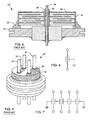
- a prior art unipolar feedthrough capacitor 20 is mounted to a hermetic terminal of an implantable medical device, such as a cardiac pacemaker, an implantable cardioverter defibrillator (ICD) a cochlear implant, or the like. It will be seen from the electrical schematic diagram in FIG. 4 that the characteristics of the feedthrough capacitor 20 of FIGS. 3 and 5 are identical to those of the capacitor 12 shown in FIG. 1 .
- Such prior art capacitors 20 are typically constructed using a silver-bearing or palladium silver bearing-glass frit for the outside diameter termination surface 22 as well as the inner diameter surface 24.
- Connecting material 26 connects the capacitor's lead wire 28 to the inside diameter surface 24 of the feedthrough capacitor 20.
- the material 26 is typically of a silver-filled conductive polyimide, or a lead or tin bearing solder or the like. If the capacitor 20 were exposed and placed on the body fluid side of the medical device, a thin film of moisture 30 would be present across the surface of the capacitor. This moisture could be present from direct immersion in body fluid or from the penetration of any adjunct sealants by body fluids. In the presence of moisture 30, dendrites or metal migration 32 would form or grow between the areas of opposite polarity 22 and 24. This dendritic growth or migration can also occur from the capacitor's outside diameter metallization material 22 and the material used to make the electro- mechanical connection between the capacitor lead wire 28, and the capacitor's inside diameter 24.
- connection material 26 which forms the electro-mechanical connection from the capacitor outside diameter 22 to a ferrule 34, could still be problematic because the connecting material 26 is typically a silver-filled conductive thermosetting polymer, such as a conductive polyimide or the like.
- the silver in the presence of moisture and a voltage bias, the silver is free to migrate and form dendrites 32 as shown in FIGS. 3 and 5 .
- dendrites 32 are highly undesirable because they are conductive and tend to lower the insulation resistance or short out the capacitor 20. This is particularly problematic in a low voltage pacemaker application where the formation of the silver, tin or other dendrites 32 would preclude the proper operation of the implanted medical device.
- Another undesirable effect of the formation of these dendrites 32 is that they would tend to conduct current and thereby dissipate power unnecessarily, leading to premature battery failure of the implanted medical device. Premature battery failure is highly undesirable and leads to unwanted surgery and increased expense, usually the replacement of the entire implantable medical device.
- a surface mounted quadpolar capacitor 36 is illustrated, such as that described in U.S. Patent No. 5,333,095 , the contents of which are incorporated herein.
- dendrites 38 or 38' can form between any points of opposite polarity as long as there is migratable material as well as a migratable medium.
- Migratable mediums include thin films of moisture, solvents or the like. Accordingly, another problem can arise during cleaning or washing of the capacitor 36. Any entrapped cleaning solvents, such as alcohol, water or degreasers, when coupled with a bias voltage, can allow for the migration of the metallic migratable materials.
- dendrites 38 form between lead wires 40 of opposite polarity, but also at 38' between two lead wires of the same polarity and an adjacent ground at the capacitor outside diameter metallization 42. Both conditions are highly undesirable in that the dendrite 38 or 38' formation could short out or reduce the insulation resistance between the two lead wires 40 thereby degrading any biological signal sensing that they may perform.
- the term "short out” does not necessarily imply that the dendrite 38 or 38' will form a zero ohm connection because the resistance of the dendrite, metal migration or whisker depends upon a number of factors including the thickness density and length of the dendrite 38 or 38' that is formed. Dendrites do not form a continuous sheet, but rather are discontinuous.
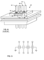
- FIGS. 8 and 9 show an in-line quadpolar capacitor 44 is illustrated wherein the outside or ground termination 46 is in two localized areas. Such localization minimizes the opportunity for dendrites to form.
- a connective material 50 which is comprised ofmigratable material, typically a silver-filled solder or conductive thermal-setting polymer such as a conductive polyimide or the like
- the formation of dendrites 52 or 52' is possible in the presence of moisture.
- a dendrite 52 could form between the capacitor conductive metallization 46 and lead wire 54, or a dendrite 52' could form between lead wires 54, as illustrated.
- FIG. 10 illustrates an internally grounded bipolar feedthrough filter capacitor 56, such as that disclosed in U.S. Patent No. 5,905,627 the contents of which are incorporated herein by reference.
- a dendrite 58' can still form if a moisture film and voltage bias form between the lead wire 60 and the ground pin 66 or a dendrite 58 can form between a lead wire 60' and a conductive ferrule 62.
- the conductive ferrule 62 has been greatly simplified and shown as a rectangular plate. In the art, these ferrules 62 take on a variety of sizes and shapes, including H-flanges to capture the mating halves of an implantable medical device housing.
- the dendrite 58 has formed all the way from the inner diameter termination surface 64 conductive material to the ferrule 62.
- an internally grounded feedthrough capacitor 56 there is always a grounded lead wire or pin 66 which is connected to the capacitor's internal electrode plate set 68, illustrated in FIG. 12 . It is also possible, or even likely, to form a dendrite 58' between this lead wire and any adjacent lead of opposite polarity. Such a dendrite 58' would short out the lead wire 60 to the grounded lead pin 66.
- the migratable material need not be present on both sides.
- a migratable material is not necessarily both the cathode and the anode.
- silver particles from conductive silver bearing glass frit fired onto the capacitor is capable of migrating in the presence of a voltage bias and a moisture film.
- a dendrite material form directly between the inside diameter metallizations 64 from the ground feedthrough hole and one or more of the active insulated feedthrough capacitor wires.
- dendrites can sometimes be very confusing for the test technician. This is because the dendrites most readily form in a high-impendence, low voltage circuit where a moisture film is present along with migratable materials.
- the dendrite, metal migration or metal whisker is typically very lacy, thin and of low cross-sectional area. Accordingly, this material can act like a fuse and open up if a high voltage or a low impedance voltage or current source is applied. Accordingly, when dendrites are present, they are sometimes inadvertently blown open by routine electrical testing either by the manufacturer or by the customer's receiving inspection department.
- FIGS. 13 and 14 show a prior art integrated chip capacitor 70, such as that described in U.S. Patent Nos. 5,959,829 and 5,973,906 , the contents of which are incorporated herein.
- These chip capacitors 70 come in a variety of sizes and shapes and are used to decouple electromagnetic interference from the lead wires 72 of an implantable medical device to the metallic ferrule 74.
- capacitor 70 has integrated four rectangular chip style capacitors into a single monolithic package. Each of these chip capacitors makes a connection to a respective lead wire 72 and decouples EMI to the metallic ferrule 74.
- dendrite 76 will form if moisture or solvents are present. Such dendrites 76 can form between the migratable connective materials used to connect the capacitor metallization 78 to the lead wire 72 and the ferrule 74, or between the lead wires 72 (not shown).
- Dendrites can also form from lead wires to the conductive materials 77 used to connect the capacitor's ground termination to the conductive ferrule.
- the ferrule is of a non-migratable material such as titanium or a noble metal, such as gold or the like, provided that the connective material 77 is of a migratable material such as silver, tin, or other known migratable metals.
- the inventors are not aware of a single instance in an implantable medical device where the capacitor has been placed on the outside and exposed to body fluid. Instead, it has been standard practice in the medical implant industry that all electronic components be protected inside the hermetically sealed enclosure, which is typically vacuum evacuated and back filled with an inert gas such as nitrogen or the like to ensure a very dry atmosphere, and prohibit contact with body fluids. Of course, in such a dry atmosphere, one of the three essential ingredients for metal migration or dendrite formation is removed and such dendrites do not form.
- Metal migration, whiskers and dendrite formation does not only occur of the surfaces on ceramic feedthrough and chip capacitors. Said dendrites can also form inside the capacitor along microfractures, cracks, or knit line defects (slight separations in the capacitor electrode lamination boundary). Internal metal migration within a ceramic capacitor can have the same catastrophic effects as surface migration. That is, the insulation resistance of the capacitor can be severely reduced including the shorting out of the capacitor completely.
- the ceramic feedthrough capacitor which acts as an EMI filter is poised directly at the point of ingress and egress of the lead wires between the implantable medical device and body tissue.
- the feedthrough capacitor is placed at the point where lead wires from the heart enter into the pacemaker itself. Any short circuiting or lowering of insulation resistance of the ceramic feedthrough capacitor precludes or shorts out the proper operation of the pacemaker itself. This can be very dangerous or even life threatening to a pacemaker-dependent patient whose heart depends on each pulse from a pacemaker so that it itself will beat.
- Pacemaker potential responses to EMI include sensing (pacemaker inhibition), noise reversion to asynchronous spacing, tracking for dual chamber devices, in rate adaptive devices the rate changes within programmed rate limits, activation of the lead switch, ICD undersensing, asynchronous pacing, or microprocessor reset.
- ICD implantable cardioverter defibrillator
- potential responses to EMI can include all of the responses for a pacemaker in that ICDs often include a pacemaker function.
- ICDs may also respond to EMI by over-sensing that manifests itself as either inhibition or an inappropriate delivery of therapy.
- An inappropriate delivery of therapy means that a fully alert and cognizant patient would receive a high voltage shock. Delivery of such a high voltage can injure the patient by literally throwing him off his feet (such a case has been documented with the male patient breaking his arm).
- ICDs can respond to EMI by tracking, undersending an arrhythmia, or electrical current directly induced in the lead system that can trigger a dangerous cardiac arrhythmia. Accordingly, proper operation of the EMI filter is critical to protect the implantable medical device from not exhibiting any of the possible aforementioned malfunctions. Formation of dendrites can seriously degrade the proper operation of the pacemaker and/or make the filter ineffective at performing its proper function.
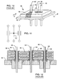
- FIGS. 15-17A a cross-sectional view of a prior art unipolar feedthrough capacitor assembly 79 is shown similar to that described in U.S. Patent Nos. 4,424,551 ; 4,152,540 ; 4,352,951 and others.
- Monolithic ceramic capacitors have a relatively low thermal coefficient of expansion compared to metals. Ceramic capacitors are very strong in compression, but very weak in tension. This is typical of most brittle materials. Accordingly, it is very easy to introduce cracks within the ceramic capacitor structure if the capacitor is subjected to excessive stresses.
- the ceramic capacitor assembly shown in FIG. 15 has the ceramic capacitor 87 embedded within a metallic ferrule 80.
- this metallic ferrule 80 would typically be made of titanium and could have a variety of shapes and flanges.
- the connection from the inside diameter of the ferrule 80 to the outside diameter termination surface metallization 82 of the feedthrough capacitor is shown as material 84.
- Material 84 is typically a thermal-setting conductive adhesive, such as a silver-filled conductive polyimide, epoxy or the like.
- the entire assembly shown in FIG. 15 is designed to be installed into a pacemaker, ICD or the like by laser welding directly into the titanium can of the implantable device. Accordingly, the ferrule 80 is rapidly heated and tends to expand. The relatively cooler ceramic capacitor 87 does not expand nearly at the same rate. Accordingly, a variety of cracks can be introduced into the ceramic capacitor. These cracks can be axial, radial or cover sheet type features.
- a crack 86 has propagated across the corner of the ceramic capacitor 87. Additionally, the crack 86 has contacted plates 88 and 90 of opposite polarity. In other words, the crack 86 has propagated through the main body of the ceramic dielectric 92 between a ground electrode plate 88 and the lower active electrode plate 90. This in and of itself does not present an immediate electrical defect. The reason for this is that as long as the crack 86 itself does not contain metallic particles, the two electrodes 88 and 90 are not shorted out. However, it is quite possible for these cracks to propagate to the outside diameter or top surface of the capacitor 87.
- FIG. 17A shows a silver dendrite 86' that has formed by metal migration through the crack.
- the reason for the formation of the dendrite has to do with the intrinsic materials that are typically used in the prior art electrodes and capacitor terminations themselves.
- Ceramic capacitors are typically made with nickel, silver or palladium silver electrodes. These are low cost electrode systems that are found in many ceramic capacitors today. They are formed within the solid monolithic ceramic by firing or sintering at a relatively low temperature (around 1100'C). An internal dendrite is a highly undesirable situation to occur because it may short out the capacitor 87.
- Such shorting or reduced insulation resistance of the ceramic capacitor 87 not only degrades its effectiveness as an EMI filter, it also can cause the catastrophic failure of the entire implantable medical device. As mentioned, this can be life threatening, for example, in the case of a pacemaker-dependant patient.
- the dendrite 86' can be low enough in resistance to short out the pacemaker output pulse. In this case, the patient's heart would simply stop beating, which would quickly lead to death.
- hermetic seal In the past, passive circuit elements such as resistors, inductors and capacitors have been enclosed within a hermetic seal. However, there are a number of negatives associated with the hermetic seal. One is, as a practical matter, the hermetic seal ends up being larger than the individual capacitor and filter components themselves. When threading the leads in the human body, particularly into the left ventricular area, or tunneling leads, for example, to a deep brain stimulator, it is important that the leads be as small as possible. A second negative associated with a hermetic seal is it adds greatly to the packaging complexity and the cost.
- connection material 26 was a silver-filled thermal-setting conductive epoxy or polyimide
- those silver particles could migrate under the presence of voltage bias in body fluid and moisture thereby resulting in a metal whisker or a dendrite and thereby creating a low impedance or even a short circuit.
- electrical connection material 26 was a lead-bearing solder
- the lead could leech into body fluids and become toxic to body tissues.
- Similar analogies apply to other electronic components, including bandstop filters, diodes, multiplexers, inductors, resistors, transistors, microchips, electronic networks and the like, such as those shown and described in U.S. Patent No. 7,363,090 , U.S. Patent Application Serial Nos.
- biocompatible and non-migratable electrical connection material and/or biocompatible thermal-setting conductive attachment material which can be used in combination with any passive or an electronic component or network, including combinations of capacitors, inductors, resistors, frequency selective networks, such as bandstop filters, transistors, microchips, RFID chips, lead based sensors, diodes, multiplexers, MEMs devices and the like.
- the present invention fulfills these needs and provides other related advantages.
- an implantable passive or active electronic network component or component network which is suitable for prolonged direct body fluid exposure and is attachable to a conductive surface, circuit trace, lead or electrode.
- the electronic network component or component network comprises (1) a non-conductive body of biocompatible and non-migratable material, (2) a conductive termination surface ofbiocompatible and non-migratable material associated with the body, and (3) a connection material of biocompatible and non-migratable material for conductively coupling the termination surface to the conductive surface, circuit trace, lead or electrode.
- connection material comprises a thermal-setting adhesive such as a polymer selected from the group consisting of epoxies, polyimides, polyethylene oxide, polyurethane, silicone, polyesters, polycarbonate, polyethylene, polyvinyl chloride, polypropylene, methylacrylate, para-xylyene, and polypyrrhol.
- a thermal-setting adhesive such as a polymer selected from the group consisting of epoxies, polyimides, polyethylene oxide, polyurethane, silicone, polyesters, polycarbonate, polyethylene, polyvinyl chloride, polypropylene, methylacrylate, para-xylyene, and polypyrrhol.
- the adhesive preferably includes a biocompatible metal filler such as a noble metal filler such as titanium, platinum and platinum/iridium alloys, tantalum, niobium, zirconium, hafnium, nitinol, Co-Cr-Ni alloys such as MP35N, Havar® and Elgiloy®, stainless steel, gold, ZrC, ZrN, TiN, NbO, TiC, TaC, Indium Oxide/Indium Tin Oxide.
- a biocompatible metal filler such as a noble metal filler such as titanium, platinum and platinum/iridium alloys, tantalum, niobium, zirconium, hafnium, nitinol, Co-Cr-Ni alloys such as MP35N, Havar® and Elgiloy®, stainless steel, gold, ZrC, ZrN, TiN, NbO, TiC, TaC, Indium Oxide/Indium Tin Oxide.
- the termination surface comprises a noble metal or a noble metal composition, or other non-migratable and biocompatible material such as titanium, platinum and platinum/iridium alloys, tantalum, niobium, zirconium, hafnium, nitinol, Co-Cr-Ni alloys such as MP35N, Havar® and Elgiloy®, stainless steel, gold, ZrC, ZrN, TiN, NbO, TiC, TaC, Indium Oxide/Indium Tin Oxide.
- a noble metal or a noble metal composition such as titanium, platinum and platinum/iridium alloys, tantalum, niobium, zirconium, hafnium, nitinol, Co-Cr-Ni alloys such as MP35N, Havar® and Elgiloy®, stainless steel, gold, ZrC, ZrN, TiN, NbO, TiC, TaC, Indium Oxide/Indium Tin Oxide.
- the biocompatible connection material comprises a brazing, welding or soldering material selected from the group consisting of: titanium, platinum and platinum/iridium alloys, tantalum, niobium, zirconium, hafnium, nitinol, Co-Cr-Ni alloys such as MP35N, Havar® and Elgiloy®, stainless steel, gold, ZrC, ZrN, TiN, NbO, TiC, TaC, Indium Oxide/Indium Tin Oxide (Transparent Conductive Oxides), gold-bearing glass frit, TiCuSil, CuSil, and gold-based braze.
- the adhesive may adhere at least a portion of the electronic network component or component network to the conductive surface, circuit trace, lead or electrode.
- the electronic network component may comprise a capacitor, a resistor, an inductor, a diode, a transistor, an electronic switch, a MEMs device, or a microchip.
- the capacitor includes first and second sets ofbiocompatible and non-migratable electrode plates embedded within the body, wherein each set of electrode plates is conductively coupled to a respective conductive termination surface.
- the first and second sets of electrode plates comprise a noble metal or noble metal composition such as gold, platinum, a gold-based alloy, or a platinum-based alloy.
- the inductor comprises at least one biocompatible and non-migratible circuit trace on a surface of the body, which extends from a first biocompatible and non-migratable termination surface to a second biocompatible and non-migratable termination surface.
- the inductor circuit trace preferably comprises a noble metal or a noble metal composition such as gold, platinum, a gold-based alloy or a platinum-based alloy.
- the inductor may comprise at least one biocompatible and non-migratable circuit trace embedded within the body and extending from a first biocompatible and non-migratable termination surface to a second biocompatible and non-migratable termination surface.
- the inductor circuit trace preferably comprises a noble metal or a noble metal composition such as gold, platinum, gold-based alloy or a platinum-based alloy.
- the aforementioned capacitor may be placed in parallel with the inductor to form a bandstop filter in accordance with the present invention.
- the resistor preferably comprises a biocompatible and non-migratable circuit trace on a surface of the body which extends from a first biocompatible and non-migratable termination surface to a second biocompatible and non-migratable termination surface.
- the resistor circuit trace preferably comprises a noble metal or a noble metal composition such as gold, platinum, a gold-based alloy or a platinum-based alloy.
- the resistor comprises at least one biocompatible and non-migratable circuit trace embedded within the body and extending from a first biocompatible and non-migratable termination surface to a second biocompatible and non-migratable termination surface.
- the resistor circuit trace preferably comprises a noble metal or a noble metal composition such as gold, platinum, a gold-based alloy or a platinum-based alloy.
- the diode preferably comprises at least one bio-compatible and non-migratable circuit trace embedded within the body and extending from a first biocompatible and non-migratable termination surface to a second biocompatible and non-migratable termination surface.
- the diode circuit trace preferably comprises a noble metal or a noble metal composition such as gold, platinum, a gold-based alloy or a platinum-based alloy.
- the electronic switch preferably comprises at least one biocompatible and non-migratable conductor embedded within the body and extending from a first biocompatible and non-migratable termination surface to a second biocompatible and non-migratable termination surface.
- the electronic switch conductor preferably comprises a noble metal or a noble metal composition such as gold, platinum, gold-based alloy or a platinum-based alloy.
- the MEMs device preferably comprises at least one MEMs conductor embedded within the body and extending from a first biocompatible and non-migratable termination surface to a second biocompatible and non-migratable termination surface.
- the MEMs conductor preferably comprises a noble metal or a noble metal composition such as gold, platinum, a gold-based alloy or a platinum-based alloy.
- the transistor preferably comprises at least one biocompatible and non-migratable circuit trace embedded within the body and extending from a first biocompatible and non-migratable termination surface to a second biocompatible and non-migratable termination surface.
- the transistor circuit trace preferably comprises a noble metal or a noble metal composition such as gold, platinum, a gold-based alloy or a platinum-based alloy.
- the microchip preferably comprises at least one biocompatible and non-migratable circuit trace embedded within the body and extending from a first biocompatible and non-migratable termination surface to a second biocompatible and non-migratable termination surface.
- the microchip circuit trace preferably comprises a noble metal or a noble metal composition such as gold, platinum, a gold-based alloy or a platinum-based alloy.
- the electronic network component or component network may include a plurality of conductive circuit traces within the non-conductive body.
- Such conductive circuit traces preferably comprise a biocompatible and non-migratable material such as gold, platinum, a gold-based alloy or a platinum-based alloy.
- An adhesive of biocompatible and non-migratable material is preferably utilized for conductively coupling at least two of the plurality of the conductive circuit traces together such as, for example, a multilayer conductor.
- the microchip may comprise an RFID inlet.
- An adhesive of biocompatible and non-migratable material is preferably utilized for conductively coupling the RFID inlet to an associated antenna.
- the present invention resides in active or passive electronic network components or component networks assemblies such as capacitors, resistors, inductors, frequency selective networks such as bandstop filters, diode or diode arrays, RFID chip-antenna assemblies, microchips, multiplexers, electronic switches, MEMs devices or the like, which are adapted for direct body fluid exposure.
- active or passive electronic network components or component networks assemblies such as capacitors, resistors, inductors, frequency selective networks such as bandstop filters, diode or diode arrays, RFID chip-antenna assemblies, microchips, multiplexers, electronic switches, MEMs devices or the like, which are adapted for direct body fluid exposure.
- the present invention resides in novel biocompatible electrical connection materials which can be used to connect externally or internally to any of the aforementioned active or passive electronic network components or component networks, including connections to conductive surfaces, circuit traces, leadwires or electrodes.
- electrodes can include, for example, the internal electrodes of a capacitor, such as a feedthrough capacitor or MLCC or an electrode in contact with body tissue for the purposes of either stimulating said body tissue or sensing biologic signals.
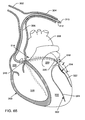
- a tissue stimulating electrode would be a pacemaker lead and electrode placed into the right ventricle of the human heart.
- a migratable material which may include silver, tin, and many other materials
- a migratable medium such as a thin film of moisture or solvent
- an activation energy such as an applied voltage.
- an active implantable medical device such as a cardiac pacemaker which is implanted in body fluid and has a small output voltage
- two of these three elements are always present; that is, the migratable medium and the activation energy.
- Activation energy is present in most active implantable medical devices, including cardiac pacemakers, implantable cardioverter defibrillators, neuro-stimulators, cochlear implants, and the like.
- solders to make the electrical connection between the active or passive electronic component or component network and its associated conductive surfaces, circuit traces, leadwires or electrodes is generally ruled out. The reason for this is that most solders contain either lead or tin, both of which are not biocompatible. The problems with lead are obvious from all of the literature regarding lead poisoning in the human body. Tin is ruled out because it is not biocompatible plus it will readily form whiskers or dendrites. Even exotic gold alloy solders still usually contain a percentage of tin or lead, which rules them out for similar reasons.
- the trouble with other conducting materials such as a conductive polyimide or conductive epoxy is that the polymer is loaded with a silver powder, such as a silver flake or a silver sphere, which is not tightly bound up chemically and is free to migrate.
- a silver powder such as a silver flake or a silver sphere
- a silver bearing glass frit which is fired onto the capacitor will readily form a dendrite.
- the third ingredient namely, migratable materials exposed to the migratable medium, be removed.
- one aspect of the present invention resides in an active or passive electronic component or component network whose electrical connections are adapted for direct body fluid exposure by being constructed of biocompatible and non-migratable materials, particularly in locations where body fluid exposure occurs.
- the active or passive electronic component or component network may also include a protective barrier, preferably glass or a non-conductive polymer coating, which helps to prevent the body fluid from contacting such conductive and critical portions of the capacitor assembly.
- a protective barrier preferably glass or a non-conductive polymer coating
- adjunct seals such as glass or polymers may be used in conjunction with biocompatible and non-migratable materials of the present invention to provide an added degree of protection.
- Biocompatible metals and alloys that can be used for the electronic network components or component network or the connection materials include all of the metals and alloys of titanium, platinum and platinum iridium alloys, tantalum, niobium, zirconium, Hafnium, nitinol, Co-Cr-Ni alloys such as MP35N, Havar®, Elgiloy®, stainless steel and gold.
- conductive metal compounds that can be used including ZrC, ZrN, TiN, NbO, TiC, TaC, and Indium Oxide/Indium Tin Oxide (Transparent Conductive Oxides).
- Commercially available biocompatible electrically conductive epoxies are manufactured by Epoxy Technology, Inc, in Billerica, MA. For example Epoxy technology EPO-TEK H81 features a biocompatible epoxy which is gold filled (www.epotek.com).
- a biocompatible and non-migratable electrical connection material can also be used to connect a terminal pin or a tissue stimulating electrode to a circuit trace or conductive surface of the electronic network component or component network.
- the conductive connection materials are typically thermal-setting, brazing, welding or special biocompatible soldering materials. So as to be non-migratable, these materials are selected from the group consisting of: gold, gold alloy, platinum, gold-filled-thermal-setting conductive material, platinum-filled-thermal-setting conductive material, gold-bearing glass frit, TiCuSil, CuSil, and gold-based braze.
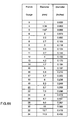
- Table 1 below shows a more comprehensive list of polymers that can also be filled with any of the biocompatible metals mentioned above.
- This list can include a variety of epoxies and polyimide materials in addition to polyethylene oxide with ionic additions such as NaCl or any of the other commonly used implantable polymers including polyurethane, silicone, polyesters, polycarbonate, polyethylene, polyvinyl chloride, polypropylene, methylacrylate, para-xylylene and polypyrrhol.
- any of these can be made conductive with a biocompatible material, for example, by adding a particulate filler such as platinum or gold flake, spheres or powder.
- a particulate filler such as platinum or gold flake, spheres or powder.
- There are other materials that could be used including pyrolytic carbon and Tra-Duct 2902 conductive adhesive.
- the passive electrical network components which include capacitors, inductors, transistors, microchips, resistors, RFID chip-antenna assemblies, and frequency selective networks such as bandstop filters, are preferably manufactured entirely of biocompatible materials in accordance with the present invention. This way they can be disposed within the lead systems of an active implantable medical device (AIMD) without the need for a separate hermetic seal casing, which is expensive and substantially increases the size of the implanted device, which is highly undesirable.
- AIMD active implantable medical device
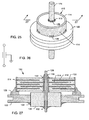
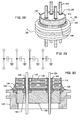
- a metal can or housing 100 is illustrated which is exemplary of those used to enclose the electronics of an implantable medical device, such as a pacemaker or the like. These electronics typically include a battery, a circuit board, integrated circuits, and a variety of other components and sensors (not shown).
- a capacitor is disposed within the housing 100, which is closed, such as by welding, and hermetically sealed to protect all of the interior electronic components from the intrusion of body fluids or other contaminants.
- Terminal pins or lead wires 102 extend into the housing 100 in insulative relationship with the housing and pass through an EMI feedthrough filter capacitor, as is well-known in the art.
- the feedthrough capacitor 104 can be disposed outside of the housing 100, advantageously saving space on the inside of the unit housing 100.
- the feedthrough capacitor 104, or any other active or passive electronic network component or component network, and the lead wires 102 are all formed of biocompatible and non-migratable materials, such as noble metals, which do not migrate in the presence of an electrical bias and body fluid.
- Another feature of the present invention is that all of the internal and external electrical connections of said capacitor or any active or passive electronic network component or component network embody electrical connection materials to adjoining surfaces, circuit traces, leadwires or electrodes, that are also designed ofbiocompatible and non-migratable materials.
- FIG. 19 an enlarged view of the lead wires 102 extending through the housing 100 is shown.
- Each of the lead wires 102 is in insulative relationship with the housing 100 by insulating material 106, which is shown for illustrative purposes.
- insulating material 106 which is shown for illustrative purposes.
- methodologies that can be used to maintain the four lead wires 102 in non-insulative relationship with the metallic can or housing 100. These include the use of alumina insulators, glass seals, or a ferrule or individual unipolar ferrules with gold-brazed alumina insulators.
- the center ground pin 108 may be hollow, as illustrated, whereby after hermetic sealing by laser welding of the lid of the housing (not shown) one could then use the hollow ground pin 108 to pull a vacuum and then back fill the inside with dry nitrogen. While still in a nitrogen tank, hollow tube 108 would then be hermetically sealed by welding, ball insertion or the like.
- the capacitor illustrated in FIG. 18 is of the internally grounded type, which simplifies the assembly. However, it is not necessary that the capacitor 104 be of internally grounded construction, but rather surface mounted technology may be used such as that described by U.S. Patent No. 5,333,095 or other capacitor types so long as they are constructed ofmaterials in accordance with the present invention so that the capacitor can be disposed in direct contact with body fluids outside of the housing 100 of the medical device.
- FIG. 21 illustrates a monolithic feedthrough ceramic capacitor 110 having metallization of non-migratable materials on an inner terminal surface 112 and an outer terminal surface 114.
- the capacitor 110 may be constructed using conventional manufacturing methods, in terms of silkscreen, punching, hole drilling, and the like.
- the metallization materials for the inner and outer termination surfaces 112 and 114 are typically comprised of a noble metal or alloy, such as pure gold, pure platinum, or the like.
- Other metals include titanium, platinum/iridium alloys, tantalum, niobium, zirconium, hafnium, nitinol, stainless steel and Co-Cr-Ni alloys such as MP35N, Havar® and Elgiloy®. See Table 1 below.
- termination surfaces 112 and 114 can be coated with the noble metals or alloys which are non-migratable, or comprised entirely of such metals. The important aspect is that those portions that are potentially in contact with moisture be of non-migratable material to prevent dendritic growth.
- TABLE 1 LIST OF CONDUCTIVE, ATTACHABLE, NON-MIGRATING BIOCOMPATIBLE MATERIALS Metals and Alloys Conductive Metal Compounds Polymers* Titanium ZrC Polyethylene Oxide with ionic addition such as NaCl (see US Patent No.
- FIG. 22 is a cross-section of the unipolar feedthrough capacitor of Fig. 21 , taken along line 22-22.
- the electrodes 116 and 118 are also formed of a biocompatible and non-migratable material.
- these electrodes 116 and 118 are constructed of platinum or a platinum alloy. The use of platinum electrodes 116 and 118 enables the capacitor to be a high fire capacitor. That is, the capacitor would have to be sintered at a much higher temperature than is typically used in the industry.
- ternary system comprised of an alloy of gold, platinum palladium, could be used.
- ternary electrodes are known, however, never in combination with the other material described herein and never used in a human implant application where direct body fluid exposure would be expected.
- the unipolar capacitor 110 is installed to a hermetic terminal 122, such as a ferrule, of a human implantable electronic device.
- a lead wire or terminal pin 124 extends through the capacitor 110, the purpose of the capacitor 110 being to prevent EMI from disturbing or interrupting the function of internal circuitry and components of the implantable medical device.
- the hermetic terminal or ferrule 122 is typically comprised of titanium or the like. While not of a noble metal or alloy thereof, titanium is biocompatible and is not migratable.
- the lead wire 124 should be coated with or solidly formed of a biocompatible and non-migratable material, typically gold or platinum or its alloys.
- the electrical connecting material 126 between the lead wire 124 and the inner termination surface 112 must also be made ofbiocompatible material that cannot migrate or form dendrites.
- the electrical connection 128 between the outer termination surface 114 and the ferrule 122 must also be comprised of a biocompatible, bio-stable, non-migratable material.
- Such electrical connections 126 and 128 are typically comprised of thermal-setting conductive adhesives, welding or soldering materials.
- thermal-setting conductive epoxies or polyimides would comprise gold, platinum or other biocompatible metals as a conductive filler.
- Said fillers may be in powder form.
- Other suitable filler materials include platinum, or platinum coated spheres or flakes of niobium or tantalum.
- the connection between the pure gold and the titanium is typically done with a gold-filled conductive polyimide.
- the connection between the lead wire 124, which may be comprised of platinum iridium, and the capacitor's inside diameter 112 which is typically comprised of gold is preferably a gold-filled conductive polyimide.
- Alternative materials, such as gold brazing compound or the like, which forms a non-migratable material, may also be used.
- gold brazed material is pure gold, pure platinum, or equivalent such that it is noble and therefore does not migrate.
- a special platinum or gold bearing fired on glass frit may also be used. See Table 1 above.
- a conductive polyimide is preferable to a conductive epoxy because of its generally higher temperature rating, although either may be used.
- An alternative to the use of a conductive thermal-setting adhesive would be the use of a non-migratable weld, braze or solder compound, such as pure gold braze or weld.
- an insulator 130 is disposed between the ferrule 122 and the lead wire 124.
- the interface between the insulator 130 and the terminal pin 124 and ferrule 122 must be hermetically sealed.
- Such seal 132 is comprised of a suitable biocompatible material such as pure gold braze or TiCuSil or CuSil. It should be noted that TiCuSil and CuSil are brazing alloys that bind up the silver so tightly that it cannot readily migrate and form a dendrite.
- the capacitor 110 and assembly illustrated in FIGS. 21-27 is comprised of materials that have been constructed of suitable biocompatible and non-migratable materials, such as noble metals, such that even in the presence of body fluid and bias voltage would not migrate and form a dendrite. That is, the capacitor inside and outside termination surfaces 112 and 114, the active and ground electrodes 116 and 118, the lead wire 124, and connective materials 126, 128 and 132 are all non-toxic and non-migratable material, at least where exposed to the body fluid. Thus, dendritic growth is prevented.
- suitable biocompatible and non-migratable materials such as noble metals
- a quadpolar surface mounted feedthrough capacitor 134 is illustrated which is entirely constructed of non-migratable materials, at least where exposed to body fluids and moisture. Thus, all of the materials exposed to the body fluid side are made of materials that will not form dendrites or migrate. That is, the portion of the lead wire 124, inner surface metallization 112, connective material 126, outer termination surface 114, and connective material 128 to the ferrule 122 which are exposed to the body fluid are comprised ofbiocompatible and non-migratable materials as described above.
- the electrodes 116 and 118 as well as the seals 132 of the insulator 130 are also comprised of such biocompatible and non-migratable materials as described above. It will be appreciated that in this and the following descriptions of various embodiments, functionally equivalent components are often referred to with the same reference number used in connection with the description of other embodiments.
- the lead wires 124 and inner and outer metallization 112 and 114 of the capacitor can be plated, such as depositing electroplated nickel first then overplating with pure gold or the like plating, or otherwise coated with the non-migratable material. Alternatively, they are comprised of such materials.
- an in-line quadpolar capacitor 136 is shown surface mounted on the body fluid side of the hermetic terminal 122 of a human implantable medical device.
- the lead wires or terminal pins 124 are coated with or formed of a non-migratable material, such as a noble metal including gold or platinum.
- the connection 126 between the inner termination surface 112 and the lead 124 is a non-migratable material, such as those described in Table 1 above.
- a hermetic terminal with gold bond pads 138 is used.
- those portions of conductive components which are exposed to the body fluid are comprised entirely ofbiocompatible and non-migratable materials to prevent the formation of dendrites.
- hermetic terminal assemblies 140 and 142 are illustrated comprised of the biocompatible and non-migratable materials as discussed above, and having a sealant 144, such as the epoxy sealant disclosed in U.S. Patent No. 6,055,455 , the contents of which are incorporated by reference herein.
- the capacitors are deliberately shown with fractures or cracks 146, resulting during the manufacturing process as described above.
- these cracks have no metal migration or dendrite within them. This is due to the fact that the capacitors are entirely constructed of materials that do not migrate. This includes the lead wire terminal pin 124, inner and outer termination surfaces 112 and 114, electrodes 116 and 118, and connective materials 126 and 128.
- a fairly large crack in a capacitor does not present a long-term reliability problem, particularly for a low-voltage device. This is due to the fact that no harmful metal migration in the form of dendrites will form.
- the penetration through the non-conductive sealing epoxy 144, shown on the top of the capacitor is not a problem. Even though it is expected that over a long period of time body fluid would penetrate through the covering epoxy 144 through bulk permeability or through micro-separations due to lack of adhesions, the capacitor and its interconnections have been all constructed in accordance with the present invention so as not to be comprised of migratable materials, thus preventing the formation of insulation resistance reducing dendrites.
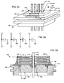
- FIGS. 36-42 show an internally grounded bipolar capacitor 148 embodying the present invention.
- the capacitor 148 is designed to be surface mounted to a hermetic terminal 122, such as the illustrated ferrule.
- Capacitor 148 has been specially prepared during manufacturing to lay down a very thin layer of glass 150 on at least its top surface, and preferably both its top and bottom surfaces, as illustrated. It has been found that such glass layers 150 not only render the overall capacitor 148 stronger so it will better resist both mechanical and thermal stress during handling, installation and assembly of the implantable medical device, but also optimizes the capacitor's 148 resistance to moisture or penetration by fluids.
- the use of a glass sealant may provide sufficient resistance to penetration by fluids so as to enable a capacitor ofmigratable materials to be placed on the body fluid side.
- the conductive components which might be exposed to the body fluid are comprised ofbiocompatible and non-migratable materials to ensure that the harmful metal migration and dendrite formation discussed above will not occur.
- Applying the glass layer 150 can be done in various manners. For example, after capacitor firing, the capacitor can be run through a glass-sealing kiln very near the melting point of the glass, but just below it. The capacitor 148 would be placed on glass sheets which would be run through the furnace allowing some of the glass to diffuse into the surfaces of the ceramic capacitor 148. The glass has the effect ofreducing some of the capacitor porosity and filling it with insulating glass. This cuts down on any tendency to form a dendrite and also makes the capacitor itself more moisture resistant. Another technique of applying the glass layer 150 would be the use of a fine glass or ground powdered glass, or a paste-like frit which would be applied to the capacitor which is then run through a firing furnace. High volume applications could be by silk-screening or spray processes. After the manufacturing of the ceramic capacitor 148 at very high temperature, it would be possible to lay down a very thin glass layer, which would be fired or co-fired into place.
- the capacitor 148 of FIG. 36 is designed to be mounted to a hermetic terminal, such as the ferrule 122 illustrated in FIG. 37 .
- This ferrule has been simplified into a rectangular shape, although in actual practice it can take have many flanges and take on many shapes and configurations depending upon its application.
- the two outer most leads 124 are formed in insulative relationship with conductive ferrule 122 by use of insulating connectors or sealants 152.
- the center lead wire, or ground wire 154 is grounded and directly brazed or welded to the conductive ferrule 122 using non-migratable material 128, such a gold braze or the like.
- the grounded pin or wire 154 which is brazed or welded to the ferrule 122 with a non-migratable material 128 is the connection point for the capacitor's internal ground electrode plates 118.
- FIGS. 39 and 40 illustrate the active and ground electrode plates used in such a configuration, such as that described in U.S. Patent No. 5,905,627 .
- the capacitor 148 and assembly are manufactured in accordance with the teachings of the present invention. That is, the internal electrode plates 116 and 118 are comprised of platinum or alloys of gold, platinum or palladium. Other electrode compositions that would not migrate in the presence of body fluids are also acceptable. Moreover, the conductive connections 126 and 128 are comprised of non-migratable thermosetting or brazing material such as that described above. The hermetic seal mechanical connections 132 are preferably comprised of a gold braze of the like. An alternative to this would be to use a glass seal where a compression or a fusion seal is formed between the ferrule and the outer lead wires 124 such that no metal joining is required at all.
- the internally grounded capacitor 148 does not require any perimeter or outer termination metallization at all. Neither does it require any electrical or mechanical connection between the capacitor 148 and the metallic ferrule 122 as this connection occurs between the ground terminal pin 154 and the ferrule 122.
- the connectors 128 between the ground lead wire 154 and the ferrule 122 are comprised of non-migratable materials, as are the seals and connectors 132 between the insulators 130 and the ferrule 122.
- the connective material 126 between in the inner diameter termination surfaces 112 and the lead wires 124 are comprised of non-migratable materials as well.
- termination materials cover both rectangular MLC chip capacitors and feedthrough chip capacitor through-hole passageways.
- the reasons for such termination metallization materials are: (1) to provide electrical connection to the active and ground electrode plates, which are set in parallel; and (2) to provide a surface wherein one can solder or otherwise make conductive attachments from the capacitor to other components in the circuitry.
- termination metallization materials are utilized in the connection from the capacitor active electrode plates and terminal pin or lead wire, and the connection between the capacitor ground electrode plates and the metallic ferrule.
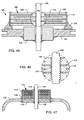
- the assembly 156 illustrated in FIG. 43 is similar to that illustrated in FIGS. 25-27 , except that the feedthrough capacitor 158 does not include an inner termination metallization surface, shown by the reference number 112 in FIGS. 25-27 . Instead, the lead wire or terminal pin 124 is conductively coupled to the set of active electrodes 116 of the capacitor 158 solely with the electrical connective material 126.
- the connective material 126 is biocompatible and non-migratable and can be comprised of such materials as gold or platinum-filled thermal-setting conductive polyimide or any other conductive material that has been loaded with suitable particles such as gold or platinum such that it can make a direct electrical contact with the one or more electrodes 116.
- the conductive thermal-setting material 126 penetrate all the way down through the one or more passageways of the feedthrough capacitor 158. This is best accomplished by injection or centrifuging. Accordingly, it is important that this material 126 not be allowed to extend underneath the capacitor 158 such that it could cause a short between the ferrule 122 or the outer metallization 114, which is still present in the embodiment illustrated in FIG. 43 . Accordingly, an insulating material or insulating washer 160 is disposed below the capacitor 158 to prevent material 126 from migrating or penetrating into areas where it would be undesirable. In a preferred embodiment, the insulating material 160 is an adhesively coated polyimide washer.
- the one or more electrodes 116 would also be of non-migratable material such as a noble metal including platinum or gold or an alternative alloy consisting of gold platinum and palladium.
- the thermal-setting conductive material 128 used to electrically connect the conductive ferrule 122 with the outer metallization 114 of the capacitor 158 is comprised of non-migratable materials as described above.
- the present invention is primarily directed to human implanted devices and applications
- the embodiment illustrated in FIG. 43 have much broader application for all feedthrough capacitors whether they be for medical implant or not.
- the concept of making electrical connection from a lead wire or to the outside diameter without the need for termination material has obvious advantages to those skilled in the art. It is very labor-intensive to apply these termination materials, which involve several process and termination firing steps. Eliminating the inner termination surface 112 and electrically coupling the lead wire 124 directly to the active electrode plates 116 with material 126 eliminates a number of process steps relating to prior art capacitor inside diameter termination material.
- FIG. 44 illustrates a terminal assembly 162 is illustrated which is similar to that illustrated in FIG. 35 .
- the feedthrough capacitor 164 embedded within the surrounding metallic ferrule 122 does not include inside diameter or outside diameter metallization (labeled with reference numbers 112 and 114 in FIG. 35 ).
- the one or more feedthrough holes which may be of any geometry, are filled with the conductive material 126 described above in relation to FIG. 43 .
- Conductive material 128, which may comprise the same material as 126, directly conductively couples the ground electrode plates 118 to the hermetic terminal ferrule 122.
- insulative material typically in the form of a washer 160, prevents shorting of the capacitor.
- FIG. 45 yet another assembly 165 is illustrated which shows an alternative method of electrically coupling a terminal pin or electrical lead 166 to the internal electrode set 116 of the capacitor 168.
- the pin or wire 166 is designed to form a very tight or pressed fit within the inside diameter or passageway of the capacitor 168.
- an inner metallization material 112 a mechanical connection is made between the lead wire 166 and the capacitor metallization 112.
- the inner metallization 112 may be absent such that the active electrode plates 116 directly contact the terminal pin or electrical lead wire 166 either through the enlargement of the terminal pin 166 or the reduction in diameter of the passageway through the capacitor 168.
- the electrical lead 166 has been prepared prior to inserting with a knurled, sputtered or roughened area 170 which coincides with the internal electrode set 116 to increase the electrical contact surface area to either the capacitor metallization 112 or directly to electrodes 116. See FIG. 46 .
- FIGS. 43-46 incorporate the non-migratable materials previously discussed so as to have application in implantable biomedical devices in which the electronic network components of the EMI filter assembly, including the capacitor, are exposed to body fluid.
- the selection and use of the non-migratable materials and the construction of the capacitor, terminal pin or lead wire, and conductive connections provide a biocompatible surface which prevents dendritic growth and the like.
- FIG. 47 illustrates an integrated feedthrough capacitor 172 such as that shown in U.S. Patent No. 6,008,980 , the contents of which are incorporated herein.
- the feedthrough capacitor 172 itself becomes its own hermetic seal. This is desirable as it eliminates a number of components and process steps. Incorporating the use ofbiocompatible and non-migratable materials in accordance with the present invention allows the capacitor 172 to be placed on the body fluid side of the hermetic seal.
- the capacitors have been feedthrough capacitors.
- the present invention is not limited to such feedthrough capacitors.
- an EMI filter assembly 173 is shown which is similar to that illustrated and described in U.S. Patent No. 5,896,267 , the contents ofwhich are incorporated by reference herein.
- the assembly 173 includes multiple leads 174 extending through feedthrough 176 and insulating film 178.
- a capacitor support assembly 180 supports two chip capacitors 182 and 184.
- Insulating film 178 is disposed between the multi-lead feedthrough 176 in the capacitor support assembly 180.
- the arrangement is applicable to feedthrough assemblies of any number of leads.
- Insulating film 178 is shaped to contour match that of the substrate 186.
- the leads 174 extend through aligned apertures 188 and 190 of the insulating film 178 and substrate 186.
- the leads 174 do not extend through the chip capacitors 182 and 184, but the chip capacitors 182 and 184 are designed so as to present active and ground electrode surfaces which interact with the leads 174 and a grounding terminal, as described in U.S. Patent No. 5,896,267 .
- the capacitors 182 and 184 and the pertinent conductive connection materials, leads 174, etc., are coated or comprised of non-migratable materials as discussed above so as to be placed on the body fluid side of the applicable implantable device outside of the hermetic terminal.
- feedthrough filter capacitor assemblies in accordance with the teachings of the present invention, namely, the use of a biocompatible and non-migratable material such as noble metals and the like, and/or glass sealing layers, allows the capacitor to be disposed outside of the housing of the medical device without tissue toxicity the formation of harmful dendrites due to metal migration.
- the free space within the housing can enable the housing to be smaller, incorporate a larger battery, more sophisticated electronics.
- novel bandstop filters consisting of a capacitor in parallel with an inductor are placed at or near the distal tip electrode in order to attenuate or prevent the flow of high frequency RF energy from an MR scanner. It has been well documented in the literature that induced RF energy from an MR scanner can cause severe damage to body tissues.
- the capacitor, inductor or resistor components and their internal and external electrical connections be manufactured entirely of biocompatible materials. This way they can be disposed within the lead systems without the need for a separate hermetic seal casing.
- Other applications include series inductors or resistors in lead wires which provide a variable reactive frequency element.
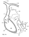
- Additional applications include remote sensors such as pulse oxygen sensors, hemodynamic or pressure sensors. These are typically placed at the end of leads inside the chambers of the heart, for example.
- biocompatible RFID sensor tags implanted within the human body ( FIG. 95 ).
- RFID chips typically include a number of passive components including inductors, capacitors and the like.
- FIG. 49 illustrates a unipolar discoidal feedthrough capacitor 110 similar to that shown in FIGS. 21-24 .
- This is a multilayer coaxial capacitor.
- One of its advantages is that it operates at very high frequency. This is because of its coaxial transmission line nature and the fact that it has very low internal inductance.
- the capacitor 110 includes overlapping circular electrode plate sets 116 and 118. Electrode plate set 116 is known as the active electrode plate set and is electrically connected to the capacitor inside diameter metallization 112 as shown.
- the ground electrode plate set 118 is attached to the outside diameter metallization 114.
- Similar feedthrough capacitors are often used in conjunction with EMI filters for active implantable medical devices. These are generally shown and described in U.S. Patents 4,424,551 ; 5,905,627 ; 6,008, 980 ; 6,643,903 ; 6,765,779 and many others.
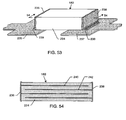
- FIGS. 50 and 51 illustrate a tubular feedthrough capacitor 200.
- this is known as a single wall or extruded tubular capacitor, and is very commonly used in commercial electronic applications.
- Such capacitors 200 are fabricated in a drawing-extrusion process.
- the tubes are cut off at a desired length and are fired (sintered).
- the material in this case is a high K ceramic dielectric 202.
- the tube is then metalized on the outside 204 and also metalized on the inside diameter 206 as illustrated.
- the capacitance is formed between the inner and outer diameter metallizations 204, 206 (two concentric cylinders separated by the high K dielectric).
- a flange 208 is typically associated with the capacitor 200 by high temperature solder attachment 210 for convenient mounting into a bulkhead.
- FIG. 52 is a cross-section of a multilayer tubular capacitor 216. This is very similar to the capacitor 200 shown in FIG. 51 except that it is not formed by tube extrusion processes.
- This capacitor 216 is rolled, has embedded electrode plates 218, 220, and has a cylindrical shape. It is then fired and metallization is placed on its top end 222 and bottom end 224 as shown. An electrical connection 226 is made to lead wire 228.
- Metallization 224 is attached to the electrode set 220 at the bottom of the cross-section.
- An optional flange 230 is added for convenient mounting into a bulkhead. This flange is attached using high temperature biocompatible and non-migratable solder, braze, thermal-setting conductive adhesive or the like 232.
- FIG. 53 is an isometric view of the rectangular monolithic ceramic capacitor (MLCC) 182 as shown in FIG. 48 . It comprises a main ceramic body 234 and it has termination surfaces 236 and 23 8 for convenient mounting to a circuit board, lead wires or the like.
- MLCC monolithic ceramic capacitor
- FIG. 54 is a cross-section of the capacitor 182 taken generally along line 54-54 in FIG. 53 .
- a resistor application one would deposit an electrode in a relatively thin trace or with relatively high resistivity materials. Accordingly, one can control a deliberately high value of resistance for certain applications.
- circuit traces 235, 237 which are typically part of a larger component network.
- Circuit traces 235, 237 would be deposited on a substrate such as alumina, polyimide or other similar biocompatible material.
- Circuit traces 235, 237 themselves, of course, must be of suitable biocompatible and non-migratable material in accordance with the present invention.
- circuit trace 237 is also functionally equivalent to a lead which could be also directly attached to the termination surface 238.
- the electrically conductive material 239 can comprise a conductive thermal-setting material comprising a polymer selected from the group consisting of: epoxies, polyimides, polyethylene oxide, polyurethane, silicone, polyesters, polycarbonate, polyethylene, polyvinyl chloride, polypropylene, methylacrylate, para-xylylene, and polypyrrhol.
- a conductive thermal-setting material comprising a polymer selected from the group consisting of: epoxies, polyimides, polyethylene oxide, polyurethane, silicone, polyesters, polycarbonate, polyethylene, polyvinyl chloride, polypropylene, methylacrylate, para-xylylene, and polypyrrhol.
- the circuit traces 235, 237 can be part of an electronic component network wherein the thermal setting material 239 has been filled with a non-migratable and biocompatible conductive material selected from the group consisting of titanium, platinum and platinum/iridium allows, tantalum, niobium, zirconium, hafnium, nitinol, Co-Cr-Ni alloys such as MP35N, Havar ® and Elgiloy ® , stainless steel, gold, ZrC, ZrN, TiN, NbO, TiC, TaC, gold-bearing glass frit, TiCuSil, CuSil, and gold-based braze.
- a non-migratable and biocompatible conductive material selected from the group consisting of titanium, platinum and platinum/iridium allows, tantalum, niobium, zirconium, hafnium, nitinol, Co-Cr-Ni alloys such as MP35N, Havar ® and Elgiloy ®
- the electrical connection 239 can also be accomplished by a brazing, welding or soldering operation consisting of materials selected from the group consisting of: tantalum, platinum, and platinum/iridium allows, tantalum, niobium, zirconium, hafnium, nitinol, Co-Cr-Ni alloys such as MP35N, Havar ® and Elgiloy ® , stainless steel, gold, ZrC, ZrN, TiN, NbO, TiC, TaC, Indium Oxide/Indium Tin Oxide (Transparent Conductive Oxides), gold-bearing glass frit, TiCuSil, CuSil, and gold-based braze.
- tantalum, platinum, and platinum/iridium allows, tantalum, niobium, zirconium, hafnium, nitinol, Co-Cr-Ni alloys such as MP35N, Havar ® and Elgiloy ® , stainless steel, gold, ZrC, Z
- FIG. 55 is an isometric drawing of a chip inductor 244 which could be used in place of a spiral wound inductor.
- the chip inductor 244 includes a thin substrate 246 which can be a biocompatible ceramic, circuit board material or the like.
- the inductor circuit trace 248 includes convenient wire bond pads 250 and 252. This is better understood by looking at the enlarged fragmented view of FIG. 56 . There, an optional wire bond pad 250a is shown which has been surface mounted. This provides another way to attach a lead wire, for example, by gold wire bonding. Also, evident from FIG. 56 is the thickness t of the inductor circuit trace 248.
- Chip inductors and chip resistors can also be wound on a cylindrical mandrel.
- this mandrel could be of ferromagnetic materials in order to increase its volumetric efficiency and the amount of inductance it has achieved.
- ferromagnetic materials are contra-indicated for MRI imaging applications. Accordingly, it's preferred that the use of wound or coaxial resistors or inductors not employ any ferromagnetic materials.
- a major problem with winding multiple turns of small diameter wire is the relatively high value ofDC resistance that would result.
- FIGS. 55 and 56 overcomes such disadvantages by providing a volumetrically efficient inductor while at the same time minimizing the DC resistance.
- FIG. 57 is an isometric view of a composite monolithic ceramic capacitor-parallel resonant TANK (MLCC-T) 254 which forms a bandstop filter 256. Viewed externally, one can see no difference between the MLCC-T 254 and an MLCC capacitor such as that illustrated in FIG. 53 . However, the novel MLCC-T 254 has an embedded inductor 258 which is connected in parallel across the capacitor between its opposite termination surfaces 236 and 238.
- MLCC-T composite monolithic ceramic capacitor-parallel resonant TANK
- FIG. 58 is an exploded view of the various layers of the MLCC-T TANK filter 254 shown in FIG. 57 .
- the MLCC TANK (MLCC-T) 254 includes an embedded inductor 258. At low frequencies, the embedded inductor 258 shorts out the capacitor from one end to the other. However, at high frequency, this forms a parallel TANK circuit 256 which is better understood by referring to the schematic diagram in FIG. 59 .
- FIG. 58 one can see that as the capacitor stacks up from the top, we have an area of blank cover sheets 260 followed by one or more embedded inductor layers 258.
- These inductor meander traces 262 can have a variety of shapes as further illustrated in Fig. 83 of U.S.
- Patent Publication No. 2007/0112398 there are a number of other blank interleafs 264 before one gets to the capacitor electrode plate sets, 240 and 242. As shown, the capacitor electrode plate set 240 connects to the left hand termination 236 and the capacitor electrode plate set 242 connects to the right hand termination 238. In FIG. 58 , only single electrodes are shown as 240, 242. However, any number of plates "n" could be stacked up to form the capacitance value that is desired. Then bottom blank cover sheets 266 are added to provide insulative and mechanical strength to the overall bandstop filter MLCC-T 254. The meander inductor trace 262 is deposited or silk screened onto the layer 258, which can be one layer or many layers as desired.
- inductor 262 itself is known as a meander because it tends to meander back and forth as it goes through the MLCC-T 254.
- the aforementioned stack up illustrated in FIG. 58 could be done both by wet-stack processing wherein each ceramic layer is sprayed down as a liquid or in a waterfall process, then predried, and then the electrical layers (other capacitor electrodes or inductor traces) are laid down and dried. In a typical ceramic capacitor thick film process, these layers are laid down in ceramic tape and then stacked and pressed. In either case, a monolithic structure is formed which is then stacked and pressed.
- the methodology that is illustrated in FIGS. 57 and 58 is also applicable to a wide range of other types of capacitor technologies including electrolytic and film.
- film capacitors can be stacked like an MLCC or rolled encompassing any of the embedded inductor traces as illustrated herein. It will also be appreciated that wound or monolithic layered film capacitors could also be constructed with an attached or embedded inductor in a similar fashion. Accordingly, the concepts of the present invention are applicable to a wide variety of equivalent electronic network component technologies.
- termination surfaces can be a biocompatible thick film ink, such as glass fitted platinum or gold, a gold plating, or the like and applied in many processes that are known in the art.
- the overall MLCC-T 254 which is illustrated in FIG. 57 , looks identical to a prior art MLCC. However, embedded within it is the novel inductor structure 258 creating the novel parallel bandstop filter 256.
- the capacitor electrode plate sets 240 and 242 can vary anywhere from two to four plates all the way up to as many as hundreds of alternating parallel plates. The number of electrode plates and their overlap area, (along with the dielectric constant and dielectric thickness) determines the capacitance value for a particular resonant bandstop filter application.
- the inductor traces 262 and the capacitor's electrode plates 240 and 242 would be of a noble metal such as pure platinum or gold which are biocompatible materials.
- bandstop filters 256 will be placed in human tissues (for a pacemaker, literally floating in the blood stream), it is very important that all of the materials, including platinum, gold, palladium, tantalum, niobium and titanium, be biocompatible and extremely reliable. Platinum is an excellent choice for such biocompatible materials and is preferred in the MLCC-T 254 of the present invention because of its excellent compatibility with the ceramic layers such as Barium Titinate, Barium Strontinate, and the like. This is because of the high melting point of the platinum. In a preferred embodiment, the ceramic materials including Barium Titinate or Barium Strontinate and the like would be lead free and would themselves be composed of entirely biocompatible materials.
- any of the inductor circuit traces 262 from FIG. 83 of US 2007/0112398 could also be printed or deposited right on top of the MLCC capacitor 182 to form MLCC-T 254'. In this case, they do not need to be embedded and co-fired within the entire ceramic capacitor.
- the advantage here is that low cost MLCCs which have been produced from very high volume commercial capacitor operations could be utilized and the inductor trace 262 could be printed on as a supplemental operation.
- the inductor trace 262 could also be placed on its own substrate which could then be co-bonded to a monolithic ceramic capacitor which is essentially equivalent to the structure previously shown in Fig. 60 .
- FIG. 61 is the schematic diagram of the FIG. 60 MLCC-T 254'.
- the inductor 258 imprinted onto the capacitor 182 could be made of pure platinum or pure gold so that it would be biocompatible and suitable for direct exposure to body fluids.
- This is a very convenient rectilinear (flat) geometry in that it is readily adaptable to electrodes that are typically used for neurostimulators, deep brain stimulators, spinal cord stimulators and the like.
- Coaxial parallel TANK circuits are more applicable to insertion through veins like the subclavian vein and down through the valves of the heart for convenient insertion into the right ventricle.
- Coaxial geometries are also particularly adapted where the physician must use surgical tunneling techniques to insert an electrode.
- tunneling techniques are commonly used for neurostimulators to insert a lead wire to stimulate a particular nerve or muscle in a paralyzed patient.
- the technology and invention described above is also applicable to any type of passive component array including low pass filters, high pass filters, bandstop filters and series resonant (L-C) trap filters.
- FIGS. 62 and 63 describe alternative ways of accomplishing the same thing using a feedthrough capacitor structure.
- the inductor 270 has been printed onto the top of the capacitor 110 or attached to the capacitor by means of a supplemental substrate.
- Lead wire 272 is connected to the capacitor's internal diameter metallization 112 using an intermediate contact plate 274.
- the electrode 276 is electrically and mechanically attached to the capacitor outside diameter metallization 114, but electrically insulated from the internal metallization 112, such as with an insulative pad or liner 278.
- FIG. 64 illustrates a chip resistor 280.
- Chip resistors can embody either thick film or thin film technology.
- FIG. 64 illustrates an implantable chip resistor 280 which comprises a nonconductive body 282 or substrate ofbiocompatible and nonmigratable material such as alumna ceramic.
- a thick or thin film resistive element 284 is deposited on top of the body 282. This forms a conductive electrode with a volume resistivity and thickness that is consistent with the overall resistance value as measured between termination surfaces 288 and 290.
- the resistivity and the thickness of the deposited layer 284 are both adjusted in order to control the overall resistance.
- the overall physical dimensions of the chip are important. For example, if the chip was longer and thinner, you would have greater resistance and so on.
- the chip electrode resistance element 284 is typically covered by a protective coating 286.
- Resistance element 284 is constructed of a biocompatible and non-migratable material in accordance with the present invention.
- Termination surfaces 288 and 290 are applied in a manner very similar to previously described monolithic ceramic capacitors (MLCCs). These conductive termination surfaces are also of biocompatible and non-migratable materials and are affixed to the main body 282. This allows for convenient electrical attachment of leadwires or circuit traces to the chip resistor 280.
- FIG. 65 is a diagrammatic representation of a human heart 300 which includes right and left subclavian veins 302 and 304 respectively, the superior vena cava 306 and the aorta 308.
- a lead wire 310 which is typically routed from a biventricular cardiac pacemaker or a biventricular implantable cardioverter defibrillator (ICD) (which are not shown), is routed through a catheter 312 and directed, in this case, through the left subclavian vein 304 and then down through the superior vena cava 306 and into the coronary sinus 314.
- the leadwire 310 must first enter the coronary sinus ostium 316 where the implanting physician selects the correct location.
- the coronary sinus 314 is actually divided into two zones: the first part (on the left) is known as the coronary sinus 314; and the second part (on the right) is called the great cardiac vein 318.
- the great cardiac vein 318 wraps around the back of the left ventricle.
- a bandstop filter 320 is intended to be placed ideally near the end of the great cardiac vein 318 where it breaks into several venous branches. These branches are called the posterior branch, the lateral branch 322 and the anterior branch 324. A more comprehensive name, for example, would be the interventricular branch.
- proximal bandstop filter 320 One can also see the right ventricle 326 and the right atrium 328. Also shown are the left atrium 330 and the left ventricle 332.
- the ideal location for a proximal bandstop filter 320 is shown.
- An ideal length for the proximal bandstop filter 320 would be between 5 and 7.5 mm in length.
- cardiac motion is relatively small and fibrotic tissue will tend to encapsulate the bandstop filter 320 and its lead wires 310 and thereby attach it/fixate it in position in this relatively low motion region. This is a particular advantage, in that the lead 310 will remain highly reliable and resistant to breakage.
- this portion of the lead wire system can be of much larger diameter (for example, 7 or 8 French as shown in FIG. 66 ).
- the great cardiac vein 318 branches the venous systems become much smaller. In general, these branches are below 6 French in diameter and ideal electrode sizes go all the way down to 3 French.
- FIG. 66 shows the relationship between French size, millimeters and inches.
- a lead wire reduction should occur at the point of egress of the bandstop filter 320 allowing insertion of electrodes into the small diameter venous system in the proper position outside the left ventricle 332.
- the primary benefit of locating the bandstop filter 320 in the coronary sinus 314 and/or great cardiac vein 318 is that the diameter of the bandstop filter 320 itself can be larger making it much easier to manufacture.
- the distal portion 334 of the lead 310 from the bandstop filter 320 is smaller (3 to 6 French size) for easier employment and navigation into the branch veins of the left ventricle 332.
- Secondary benefits beyond the diameter of the bandstop filter 320 include the length of the bandstop filter. Entering into and navigating the coronary sinus 314 and great cardiac vein 318 generally involve larger bend radii compared to accessing and navigating the branch vessels.
- the portion of the lead 334 that traverses through and resides in the branch vessels must be very small and very flexible, not having a stiff section longer than approximately 1.5 mm as a rule of thumb.
- Rigid sections of the lead 310 measuring longer than 1.5 mm can impede the ability to navigate around the tight corners and bends of the branch vessels.
- stiff sections of the lead could approach 5 mm or even 7.5 mm without drastically impeding deliverability.
- a secondary benefit of locating the bandstop filter 320 in the coronary sinus 314 or the great cardiac vein 318 has to do with MRI image artifacts.
- the image artifact will be quite small due to avoiding the use of ferromagnetic materials, it is still beneficial to locate the bandstop filter 320 away from the coronary arteries, ventricular wall motion or other anatomies/physiologies/pathologies of most interest. If a bandstop filter 320 is located in the coronary sinus 314, however, it could generate small artifact in the vicinity of the valves. Another benefit of having the bandstop filter 320 located in the coronary sinus314 or the great cardiac vein 318 is that its rigidness provides a foundation on which fixation fixtures may be more strategically utilized. For example, one or more tines could originate from the region of the lead where the bandstop filter 320 resides.
- rigidness of the bandstop filter 320 makes the tines more effective in their engagement of the vessel walls.
- a rigid portion of the lead 360 skillfully navigated beyond a corner or bifurcation, can function as a fixation mechanism that proves difficult or requires skill to track the lead.
- FIG. 67 is an enlarged perspective view of the lead wire system 310 taken from FIG. 65 .
- a guide wire 336 which is common in the prior art for inserting into position prior to sliding the lead wire system 310 down over it.
- a terminal pin 33 8 is designed to plug into the implantable medical device, such as a pacemaker or ICD.
- the bandstop filter 320 is shown at the point where the lead wire 310 would be reduced from 6-9 French down to 3-6 French.
- Optional fixation tines 340 are shown which may be affixed to the bandstop filter 320.
- the French scale is related to both diameter in millimeters (mm) or inches.
- the length (l) of the reduced diameter lead wire section 334 can be adjusted in accordance with the branch vein into which the lead system is being inserted in the desired location of the electrodes 342. Below the electrodes 342 is the other end of the guide wire 336. Once the electrodes 342 are in the proper position and the system has been tested, the guide wire 336 is typically removed.
- a particular advantage of the lead system 310 as shown in FIG. 67 is that no new deployment instruments or catheters are required. In other words, this system that includes the bandstop filter 320 is backwards compatible with all known deployment systems.
- the lead wire system 310 is designed to be extracted in the case of a broken lead, defective lead or infected lead.
- the lead wire system illustrated in FIGS. 67 and 68 is also backwards compatible with current (prior art) mechanical and laser lead extraction technologies.
- FIG. 69 illustrates a multilayer flex cable 344 onto which capacitor 346 and monolithic ceramic chip inductor 348 are mounted. Internal circuit traces place the inductor 348 and the capacitor 346 in parallel forming the bandstop filter 350 as shown in the schematic diagram of FIG. 70 . This forms an inline bandstop filter which is very suitable for placement within the distal electrode illustrated in FIGS. 67 and 68 . In FIG. 69 one can see that the entire bandstop filter assembly is not hermetically sealed. This is particularly desirable to keep the French gauge size as small as possible. There are electrical connections 352-362, all of which are biocompatible and are formed of non-migratable materials in accordance with the present invention.
- FIG. 71 is a cross-sectional view taken generally from line 71-71 of FIG. 69 , wherein one can see the cross-section of the inductor 348 and the capacitor 346 and also the circuit flexible substrate 364.
- an insulating material 366 which is generally a thermal setting non-conductive biocompatible polymer which provides protection and mechanical robustness to the overall package.
- FIG. 72 illustrates an alternative embodiment wherein a flexible circuit substrate 364' is shown.
- the circuit substrate be laying flat while the pick and place robots place the inductor and the capacitor components. As illustrated in FIG. 73 , this is then folded up so that it will fit conveniently into a cylinder or other suitable protective housing.
- electrical connections 352-358 which again are a biocompatible non-migratable material in accordance with the present invention.
- conductive surfaces 368 and 370 As shown in FIG. 73 , these can also be folded back. These conductive surfaces are convenient for attachment into the leadwire system as previously described in FIGS. 65 , 67 and 68 .
- laser welds 372 and 374 which are used to attach a typical NP35N alloy leadwire 316 to the bandstop filter structure.
- Laser welding ofbiocompatible materials meets all of the requirements of the present invention as to biocompatibility and non-migratable materials.
- FIG.74 is a diagrammatic representation of the human heart similar to that illustrated in FIG. 65 .
- external (epicardial) electrodes 378 are attached outside and to the left ventricle 332 by means of epicardial leads 380.
- a sutureless myocardial lead 380, 382 is shown affixed to the outside of the left ventricle 332.
- This methodology is well known and generally involves an insertion between the ribs outside of the heart and a screwdriver type feature to affix the sutureless epicardial lead tip electrode 378 in place.
- Epicardial leads may also have a suture feature which is also well known in the art, which can have a helical or other configuration type tip.
- the present invention can be extended to any type of external (epicardial) electrode 378 or satellite pacer affixed to the outside of the heart, particularly outside of the left ventricle.
- FIG. 75 is a cross-sectional view taken generally along line 75-75 of FIG. 74 , illustrating an epicardial lead electrode assembly 378 which includes a bandstop filter 384.
- the epicardial lead electrode assembly 378 is typically over-molded with silicone rubber 386 ( FIG. 76 ).
- the assembly shown in FIG. 75 is self-affixing to the myocardial tissue by a helical electrode structure 388.
- this electrode is affixed into the myocardium by 31 ⁇ 2 mechanical turns and is made of platinum-iridium alloy or equivalent biocompatible material.
- the helical electrode tip 388 is affixed into the myocardial tissue by a screwdriver type turning surgical tool.
- the bandstop filter 384 as illustrated in FIG.
- FIG. 75 is taken generally from Fig. 42 of U.S. Patent Application Publication No. 2007/0112398, filed November 9, 2006 .
- Almost all of the other bandstop filter embodiments that are disclosed in U.S. Patent Application Publication No. 2007/0112398 can be incorporated into the epicardial lead 378 in FIG. 75 .
- the bandstop filters shown in U.S. Patent Application Publication No. 2007-0112398 , FIGS. 35 , 37 , 42 , 58 , 65 , 69 , 70 , 80 , 85 , 87 , 94 ,115,118,128,130,132,133, 141, 142, 149, 151, 156, 157, as well as any of the designs of U.S. Provisional Patent Application No. 60/968,662 are all readily adaptable into the bandstop filter 320 and 384.
- FIG. 76 is very similar to the epicardial lead electrode assembly 318 shown in FIG. 75 , except that it has a novel ring structure 390 associated with a bandstop filter chip 384.
- This epicardial bipolar electrode also has a bandstop filter 384' in series with its helical tip electrode 388.
- a screwdriver type head mechanism can be added for convenient adapting to prior art deployment instruments. Any of the cylindrical bandstop filters described in U.S. Provisional Patent Application No. 60/968,662, filed August 29, 2007 , can also readily adapted to any of the novel bandstop filter applications described herein.
- FIG. 77 illustrates a split cylinder cuff electrode 392 embodying two electrodes (Anode (a) and Cathode (c)). This is designed to be inserted by a physician around a nerve It is a bipolar system typically consisting of a 6-8 French diameter lead body 394. A double bandstop filter chip 396 (two discrete bandstop filter chips in parallel) in accordance with the present invention is located as shown. In general, the cuff 392 is sized to match the diameter of the nerve which passes through its center. The lead body 394, after the double bandstop filter 346, is of a reduced diameter, generally in the 3-4 French range. Not shown is a closing suture which is typically used to draw the cuff together after it's installed.
- FIG. 78 illustrates helical nerve cuffs 398 which are self-sizing. These incorporate electrode foils 400 which are well known in the art.
- the lead body 402 is attached to a bandstop filter 404. This can be unipolar or bipolar as shown.
- the electrode foil 400 can either be etched or stamped and then the termination point where the conductor attaches to the foil is either prepared or fabricated. This is the location to where the bandstop filter 404 is electrically attached and incorporated.
- the conductors and the foil 400 on the bandstop filter 404 are laid into a split mold and assembled and then silicone is injected into the mold.
- FIG. 78 illustrates one leg of a bipolar or multipolar lead. Obviously, a bandstop filter 404 would be required for each electrode foil in the multipolar configuration.
- FIG. 79 is a sectional view taken generally along line 79-79 of FIG. 78 .
- FIG. 80 illustrates a larger multiple cuff nerve electrode 406 for current steering in a large nerve trunk.
- Various electrodes can be stimulated by trial and error to obtain the optimal result. For example, for pain control, one can try various electrodes and various types of electrical stimulation by trial and error until pain is minimized or eliminated.
- the multiple parallel filter electrodes 408, similar to that described in FIG. 75 can be placed in conjunction with each one of the conductors 410 as shown.
- FIG. 81 illustrates an alternative in that a multiple bandstop filter array 412 is shown in series with the lead body 414. This can in turn be connected to the cuff electrode 406 of FIG. 80 or to the multiple cuff electrodes 392,398 illustrated in FIGS. 77 and 78 . It can also be adapted to the multiple single electrodes illustrated in FIG. 82 .
- the multiple bandstop chip as illustrated in FIGS. 81 and 82 can be made in a variety of ways utilizing the technology disclosed in U.S. Patent Application Publication No. 2007/0112398 , and U.S. Provisional Patent Application No. 60/968,662 , by putting the devices on a substrate next to each other on each lead wire.
- the structure shown in FIGS. 81 and 82 can be over-molded with silicone or the like to provide reliable mechanical attachment and additional protection from body fluids.
- Fig. 83 is taken generally along the line 83-83 from FIG. 81 , and illustrates one of many ways to form a multiple array 416 of bandstop filter chips.
- a thin substrate 418 which can be of alumina or any other biocompatible substrate material known in the prior art.
- a substrate could also be a flexible substrate, such as a polyimide flex cable.
- the various meanders on the bandstop filters are for illustration only. Any active or passive electronic network component or component network of the present invention can be similarly designed.
- Different types of bandstop filters 420a-f(MRI chips) are shown by way of illustrating that there are many ways to construct this multiple array 416. Referring to drawings from U.S. Patent Application Publication No.
- the MRI chips 420a-f are similar to FIGS. 80-85 and FIG.136 (which is thick film deposited right on the substrate). Imbedded or MEMs components can also be used to form the multiple bandstop MRI filter array 416. In addition, multilayer substrates may be used to increase packaging density. Wirebond pads 422, leadwires 424 and 424' and electrical connections 426 (typically laser welds or gold wirebonds), are also shown. The bandstop filter chips 424a-f have end terminations 428 as shown. There are electrical connections from these end terminations 428 to the circuit traces 430.
- the entire assembly is desirably over coated, over molded (with silicone or the like), or glass encapsulated to enhance mechanical strength and biocompatibility.
- Every one of the active or passive electronic network component or component network electrical connections 426 must be done with a suitable biocompatible and non-migratable electrical connection material in accordance with the present invention.
- a suitable biocompatible and non-migratable electrical connection material in accordance with the present invention.
- FIG. 84 is a diagrammatic side cross-sectional view of the human head showing the skull 432 and the brain 434.
- a burr hole 436 is drilled through the skull 432 for placement of deep brain probe 438 with associated electrodes 440.
- One or more bandstop filter chips of the present invention are located inside of the skull burr hole 436.
- the top of the deep brain probe438 and associated bandstop filter would be flush with the top of the skull 432.
- the lead wire 442 is generally connected to a pulse generator or transmitter which is either implanted or can sit outside the skin. There can also be a receiver which sits on the skin.
- the deep brain probe 438 can also have a nail head or nail shank.
- FIG. 85 is an enlarged sectional view of the area indicated by line 85 in FIG. 84 , of the deep brain probe 438. Shown is the location of the bandstop filter 444, the skin 446 which covers the skull 432, the lead wire 442, the burr hole 436, dura layer 448 and the brain 434. At the end of the deep brain probe 438 are electrodes 440. Referring to the bandstop filter element 444 of FIG. 85 , one can see that it's an inline bandstop filter constructed in a way that was described in connection with FIGS. 69 through 72 . There are a number of electrical connections in FIG.
- each one of the leadwires has to be connected to either the component or conductive circuit or circuit trace and that each one of the inductor and capacitor elements must be in turn similarly connected.
- electrode leadwires450 must be connected on the other end. All of these electrical connections are of suitable biocompatible and non-migratable materials in accordance with the present invention.
- FIG. 86 is taken generally from section 86 of FIG. 85 .
- Shown is an electronic circuit board 452 which is embedded within the electronics module 444.
- bandstop filters consisting of an inductor L in parallel with a capacitor C.
- transient voltage suppressor TVS which is in parallel with each one of the bandstop filter circuits. As described in U.S. Provisional Patent Application No. 61/079,693 , this provides protection against automatic external defibrillation (AED) events.
- AED automatic external defibrillation
- all of the components are disposed upon circuit board or circuit flex cable 452.
- some of the electrical connections 454-472 which are of course, biocompatible and non-migratable in accordance with the present invention.
- each one of the circuit elements Internal and external electrical connections to each one of the circuit elements (not shown) are also required in accordance with the present invention. These would be the connections to, for example, the capacitor element metallization on each end.
- the TVS circuit would provide protection against all types of high voltage transients which could damage delicate electronic circuits. This would be particularly important if the L and C resonator elements were of delicate MEMS type structures.
- FIG. 87 is a cross-sectional view illustrating one form of the novel electronic switch 474 of the present invention.
- the distal TIP electrode pad 480 has a laser weld or equivalent biocompatible electrical attachment 482 to the surrounding metallization 484 of the ceramic insulator structure 480.
- the electrode pad 480 is electrically connected to the cathodic contact 486 of the MEMS switch 476.
- the cathodic contact 486 is rigid in this case and is not free to move.
- Lead wire 488 is then routed through the flexible neurostimulator pad insulation/encapsulant 490 and is electrically connected to the anodic MEMs contact cantilever 492 as shown.
- the MEMS switch 476 is shown in the up or open state wherein no currents can flow through it. This is the ideal position for MRI imaging or other procedures such as surgical electrocautery (Bovi knife for example) requiring high RF energy.
- Fig. 88 shows the MEMS switch 476 of FIG. 87 in the down or closed state. In this position, biological sensing and therapy signals freely pass through the switch 474.
- electrical connection material 494 and 494' which is required to attach leadwires 488 and 488' to the MEMs switch assembly.
- FIG. 89 illustrates the novel electronic switch assembly 474 of the present invention shown in an encapsulated switch assembly or module 496 convenient for location anywhere in the lead wire 498 circuit.
- the entire module 496 has been overlaid with a suitable glass seal 500.
- This glass seal 500 can be deposited as a frit or molten and then sintered at high temperature.
- the glass 500 is designed to adhere to the substrate 502 and the wire bond pads 504 and 506 such that it forms an adjunct partial hermetic seal over the entire switching circuitry 496'.
- Material 500 can be any number of borosilicate or compression glasses or even polymer sealants such as silicone and the like. Electrical connections 508-514 are shown in accordance with the present invention.
- FIG. 90 is an electrical schematic drawing of the MEMs switch assemblies previously illustrated in FIGS. 87, 88 and 89 .
- FIG. 91 illustrates a novel electronic multiplexing circuit 516. By way of illustration, a single MEMS switch 476 is shown. After the physician determines which of the multiple mini electrodes 518 is the optimal one by using the multiplexing function 520, the physician or technician can switch in the electronic switch 476 in series with that particular circuit. This has the effect of greatly reducing the number of electronic switches required.
- FIG. 92 illustrates a typical PNP transistor which could be used as part of the electronic switches as previously illustrated in FIG. 91 .
- Biocompatible transistors can be made ofbiocompatible materials with suitable biocompatible and non-migratable electrical connections.
- FIG. 93 illustrates an inductor chip 522 shown attached to circuit traces 524 and 524'. Referring to the inductor chip 522, one will see that it has metallization bands 526 and 528 as shown. In accordance with the present invention, these metallization bands would be of gold, platinum or other suitable noble or biocompatible or non-migratable material. In addition, there are electrical connections 530 and 532 which are also of biocompatible and non-migratable material in accordance with the present invention.
- FIG. 94 is an exploded view of the inductor chip 522 in FIG. 93 .
- inductor trace 536 is to be placed on substrate layer 540 and inductor trace 538 is disposed on layer 542. These are designed to be electrically in series by use of a conductively filled via hole which is continuous through 544 and 544'.
- the inductor trace material 536and 538 must be of suitable biocompatible and non-migratable material in accordance with the present invention, such as platinum or gold or the like.
- Electrically conductive filler material which fills the via hole must also be of suitable biocompatible and non-migratable material in accordance with the present invention. This is a way of illustrating the importance that both the external electrical connections 530 and 532 as previously illustrated in FIG. 93 , as well as the internal electrical connection, such as in via hole 544-544' are all equally important to achieve long term biocompatibility.
- FIG. 95 is the electrical schematic of the inductor chip 522 illustrated in FIGS. 93 and 94 .
- FIG. 96 is a diagrammatic view of an RFID chip or inlet 546 and its associated antenna 548. Shown is a Wheeler spiral antenna 548 which is terminated at electrical connection 550'. It is also connected to the integrated circuit or microchip or integrated circuit (552) at location 554. There are also suitable electrical connections 556 and 558 which connect to the opposite end of the antenna trace. There is also a loop antenna connection which forms a dipole back at location 560.
- the microchip and the wiring of the antenna would be of suitable biocompatible and non-migratable materials. Equally important is that all of the electrical connections be also of biocompatible and non-migratable materials of the present invention.
- all of the passive electrical network components namely, the capacitors, inductors, resistors and bandstop filters illustrated in FIGS. 49-91 are adapted for direct body fluid exposure by including components such as the electrode plates, inductor traces and connection materials, which comprise non-migratable and biocompatible materials.
- any components associated with the passive electrical network components shown must likewise comprise a non-migratable and biocompatible material at least where exposed to body fluid.
- components such as the electrode plates, the inductor tracing, metallization surfaces, and other surfaces which may be directly exposed to body fluids, such as the outer surface of the terminal pin preferably comprise a noble metal or a noble metal composition.
- the structures may be comprised of gold, tantalum, niobium, platinum, a gold-based alloy or a platinum-based alloy.
- leadwire attachment is necessary, such wiring would also need to be ofbiocompatible and nonmigratable materials which include gold, platinum, MP-35N or equivalent.
- biocompatible and non-migratable materials avoid the harmful formation of dendrites as explained above.
- conductive metal compounds include all of the metals and alloys of titanium, platinum, and platinum iridium alloys, tantalum, niobium, zirconium, hafnium, nitinol, Co-Cr-Ni alloys such as MP35N, Hava r® , Elgilo y® , stainless steel and gold.
- conductive metal compounds including ZrC, ZrN, TiN, NbO, TiC, TaC, and Indium Oxide/Indium Tin Oxide (Transparent Conductive Oxides).
- connection materials used to connect the passive electrical network components to other components are typically thermal-setting, brazing, welding or soldering materials. So as to be non-migratable, these materials are selected from the group consisting of: gold, gold alloy, platinum, gold-filled-thermal-setting conductive material, platinum-filled-thermal-setting conductive material, gold-bearing glass fit, TiCuSil, CuSil, and gold-based braze.
- Table 1 above shows a more comprehensive list of polymers that can also be filled with any of the biocompatible metals mentioned above.
- This list can include a variety of epoxies and polyimide materials in addition to polyethylene oxide with ionic additions such as NaCl or any of the other commonly used implantable polymers including polyurethane, silicone, polyesters, polycarbonate, polyethylene, polyvinyl chloride, polypropylene, methylacrylate, para-xylylene, and polypyrrhol.
- any of these can be made conductive with a biocompatible material, for example, by adding a particulate filler such as platinum or gold powder.
- a particulate filler such as platinum or gold powder.
- There are other materials that could be used including pyrolytic carbon and Tra-Duct 2902 conductive adhesive.
- the present invention comprises an implantable passive or active electronic network component or component network is provided which is suitable for prolonged direct body fluid exposure and is attachable to a conductive surface, circuit trace, lead or electrode.
- the electronic network component or component network comprises (1) a non-conductive body of biocompatible and non-migratable material, (2) a conductive termination surface of biocompatible and non-migratable material associated with the body, and (3) a connection material of biocompatible and non-migratable material for conductively coupling the termination surface to the conductive surface, circuit trace, lead or electrode.
- connection material comprises a thermal-setting adhesive such as a polymer selected from the group consisting of epoxies, polyimides, polyethylene oxide, polyurethane, silicone, polyesters, polycarbonate, polyethylene, polyvinyl chloride, polypropylene, methylacrylate, para-xylyene, and polypyrrhol.
- a thermal-setting adhesive such as a polymer selected from the group consisting of epoxies, polyimides, polyethylene oxide, polyurethane, silicone, polyesters, polycarbonate, polyethylene, polyvinyl chloride, polypropylene, methylacrylate, para-xylyene, and polypyrrhol.
- the adhesive preferably includes a biocompatible metal filler such as a noble metal filler such as titanium, platinum and platinum/iridium alloys, tantalum, niobium, zirconium, hafnium, nitinol, Co-Cr-Ni alloys such as MP35N, Havar® and Elgiloy®, stainless steel, gold, ZrC, ZrN, TiN, NbO, TiC, TaC, Indium Oxide/Indium Tin Oxide.
- a biocompatible metal filler such as a noble metal filler such as titanium, platinum and platinum/iridium alloys, tantalum, niobium, zirconium, hafnium, nitinol, Co-Cr-Ni alloys such as MP35N, Havar® and Elgiloy®, stainless steel, gold, ZrC, ZrN, TiN, NbO, TiC, TaC, Indium Oxide/Indium Tin Oxide.
- the termination surface comprises a noble metal or a noble metal composition, or other non-migratable and biocompatible material such as titanium, platinum and platinum/iridium alloys, tantalum, niobium, zirconium, hafnium, nitinol, Co-Cr-Ni alloys such as MP35N, Havar® and Elgiloy®, stainless steel, gold, ZrC, ZrN, TiN, NbO, TiC, TaC, Indium Oxide/Indium Tin Oxide.
- a noble metal or a noble metal composition such as titanium, platinum and platinum/iridium alloys, tantalum, niobium, zirconium, hafnium, nitinol, Co-Cr-Ni alloys such as MP35N, Havar® and Elgiloy®, stainless steel, gold, ZrC, ZrN, TiN, NbO, TiC, TaC, Indium Oxide/Indium Tin Oxide.
- the biocompatible connection material comprises a brazing, welding or soldering material selected from the group consisting of: titanium, platinum and platinum/iridium alloys, tantalum, niobium, zirconium, hafnium, nitinol, Co-Cr-Ni alloys such as MP35N, Havar® and Elgiloy®, stainless steel, gold, ZrC, ZrN, TiN, NbO, TiC, TaC, Indium Oxide/Indium Tin Oxide (Transparent Conductive Oxides), gold-bearing glass frit, TiCuSil, CuSil, and gold-based braze.
- the adhesive may adhere at least a portion of the electronic network component or component network to the conductive surface, circuit trace, lead or electrode.
- the electronic network component may comprise a capacitor, a resistor, an inductor, a diode, a transistor, an electronic switch, a MEMs device, or a microchip.
- the electronic network component or component network may include a plurality of conductive circuit traces within the non-conductive body.
- Such conductive circuit traces preferably comprise a biocompatible and non-migratable material such as gold, platinum, a gold-based alloy or a platinum-based alloy.
- An adhesive ofbiocompatible and non-migratable material is preferably utilized for conductively coupling at least two of the plurality of the conductive circuit traces together such as, for example, a multilayer conductor.
Landscapes
- Health & Medical Sciences (AREA)
- Engineering & Computer Science (AREA)
- Life Sciences & Earth Sciences (AREA)
- Biomedical Technology (AREA)
- Nuclear Medicine, Radiotherapy & Molecular Imaging (AREA)
- Radiology & Medical Imaging (AREA)
- Animal Behavior & Ethology (AREA)
- General Health & Medical Sciences (AREA)
- Public Health (AREA)
- Veterinary Medicine (AREA)
- Heart & Thoracic Surgery (AREA)
- Power Engineering (AREA)
- Manufacturing & Machinery (AREA)
- Cardiology (AREA)
- Neurology (AREA)
- Neurosurgery (AREA)
- Microelectronics & Electronic Packaging (AREA)
- Orthopedic Medicine & Surgery (AREA)
- Biophysics (AREA)
- Electrotherapy Devices (AREA)
Applications Claiming Priority (2)
| Application Number | Priority Date | Filing Date | Title |
|---|---|---|---|
| US12/269,255 US7917219B2 (en) | 2002-02-28 | 2008-11-12 | Passive electronic network components designed for direct body fluid exposure |
| US12/472,222 US8660645B2 (en) | 2002-02-28 | 2009-05-26 | Electronic network components utilizing biocompatible conductive adhesives for direct body fluid exposure |
Publications (3)
| Publication Number | Publication Date |
|---|---|
| EP2194548A2 true EP2194548A2 (de) | 2010-06-09 |
| EP2194548A8 EP2194548A8 (de) | 2011-01-12 |
| EP2194548A3 EP2194548A3 (de) | 2011-01-26 |
Family
ID=41545894
Family Applications (1)
| Application Number | Title | Priority Date | Filing Date |
|---|---|---|---|
| EP09014026A Withdrawn EP2194548A3 (de) | 2008-11-12 | 2009-11-10 | Elektronische Netzwerkkomponenten und Komponentennetzwerk mit biokompatiblen leitfähigen Klebstoffen zur direkten Körperflüssigkeitsexposition |
Country Status (2)
| Country | Link |
|---|---|
| US (1) | US8660645B2 (de) |
| EP (1) | EP2194548A3 (de) |
Cited By (1)
| Publication number | Priority date | Publication date | Assignee | Title |
|---|---|---|---|---|
| WO2012112490A1 (en) * | 2011-02-17 | 2012-08-23 | Boston Scientific Neuromodulation Corporation | Systems for making and using electrical stimulation systems with improved rf compatibility |
Families Citing this family (93)
| Publication number | Priority date | Publication date | Assignee | Title |
|---|---|---|---|---|
| US8244370B2 (en) | 2001-04-13 | 2012-08-14 | Greatbatch Ltd. | Band stop filter employing a capacitor and an inductor tank circuit to enhance MRI compatibility of active medical devices |
| US20070088416A1 (en) * | 2001-04-13 | 2007-04-19 | Surgi-Vision, Inc. | Mri compatible medical leads |
| US8219208B2 (en) | 2001-04-13 | 2012-07-10 | Greatbatch Ltd. | Frequency selective passive component networks for active implantable medical devices utilizing an energy dissipating surface |
| US8712544B2 (en) | 2001-04-13 | 2014-04-29 | Greatbatch Ltd. | Electromagnetic shield for a passive electronic component in an active medical device implantable lead |
| US8457760B2 (en) * | 2001-04-13 | 2013-06-04 | Greatbatch Ltd. | Switched diverter circuits for minimizing heating of an implanted lead and/or providing EMI protection in a high power electromagnetic field environment |
| US7211103B2 (en) * | 2002-04-11 | 2007-05-01 | Second Sight Medical Products, Inc. | Biocompatible bonding method and electronics package suitable for implantation |
| US7645262B2 (en) * | 2002-04-11 | 2010-01-12 | Second Sight Medical Products, Inc. | Biocompatible bonding method and electronics package suitable for implantation |
| EP1786320B1 (de) * | 2004-07-27 | 2016-09-14 | MRI Interventions, Inc. | Mri-systeme mit mri-kompatiblen universellen ablieferungskanülen mit kooperierenden mri-antennensonden und diesbezügliche systeme und verfahren |
| JP4912304B2 (ja) * | 2004-08-09 | 2012-04-11 | ザ ジョンズ ホプキンス ユニヴァーシティ | 埋め込み可能なmri適合刺激リード及びアンテナ並びに関連するシステム |
| US8802183B2 (en) | 2005-04-28 | 2014-08-12 | Proteus Digital Health, Inc. | Communication system with enhanced partial power source and method of manufacturing same |
| CA2789262C (en) | 2005-04-28 | 2016-10-04 | Proteus Digital Health, Inc. | Pharma-informatics system |
| EP1878091B1 (de) * | 2005-05-04 | 2017-02-22 | Boston Scientific Neuromodulation Corporation | Verbesserte elektrische leitung für eine elektronische einrichtung wie etwa eine implantierbare einrichtung |
| US7889020B2 (en) * | 2005-10-19 | 2011-02-15 | Avx Corporation | Asymmetrical filter |
| US8055351B2 (en) * | 2005-10-21 | 2011-11-08 | Boston Scientific Neuromodulation Corporation | MRI-safe high impedance lead systems |
| US8956287B2 (en) | 2006-05-02 | 2015-02-17 | Proteus Digital Health, Inc. | Patient customized therapeutic regimens |
| SG175681A1 (en) | 2006-10-25 | 2011-11-28 | Proteus Biomedical Inc | Controlled activation ingestible identifier |
| US9031670B2 (en) | 2006-11-09 | 2015-05-12 | Greatbatch Ltd. | Electromagnetic shield for a passive electronic component in an active medical device implantable lead |
| EP3785599B1 (de) | 2007-02-01 | 2022-08-03 | Otsuka Pharmaceutical Co., Ltd. | Systeme mit einnehmbaren ereignismarkern |
| WO2008101107A1 (en) | 2007-02-14 | 2008-08-21 | Proteus Biomedical, Inc. | In-body power source having high surface area electrode |
| JP5568316B2 (ja) * | 2007-03-19 | 2014-08-06 | ボストン サイエンティフィック ニューロモデュレイション コーポレイション | Mri/rf適合リード線、および関連のリード線を操作、作製する方法 |
| ES2615402T3 (es) | 2007-03-19 | 2017-06-06 | Boston Scientific Neuromodulation Corporation | Cables compatibles con IRM y RF |
| US8540632B2 (en) | 2007-05-24 | 2013-09-24 | Proteus Digital Health, Inc. | Low profile antenna for in body device |
| EP2313002B1 (de) | 2008-07-08 | 2018-08-29 | Proteus Digital Health, Inc. | Datengrundlage für einnehmbare ereignismarker |
| EP2349453A4 (de) * | 2008-10-30 | 2015-07-01 | Greatbatch Ltd | Physikalisch seriell angeordnete kondensator- sowie induktorelemente mit parallel geschalteten konzentrierten parametern zur formung eines kerbfilters |
| US9659423B2 (en) | 2008-12-15 | 2017-05-23 | Proteus Digital Health, Inc. | Personal authentication apparatus system and method |
| JP2012514799A (ja) | 2009-01-06 | 2012-06-28 | プロテウス バイオメディカル インコーポレイテッド | 摂取に関連するバイオフィードバックおよび個別薬物療法の方法およびシステム |
| WO2010129288A2 (en) | 2009-04-28 | 2010-11-11 | Proteus Biomedical, Inc. | Highly reliable ingestible event markers and methods for using the same |
| TWI517050B (zh) | 2009-11-04 | 2016-01-11 | 普羅托斯數位健康公司 | 供應鏈管理之系統 |
| EP2531099B1 (de) | 2010-02-01 | 2018-12-12 | Proteus Digital Health, Inc. | Datensammelsystem |
| EP2544634A4 (de) * | 2010-03-10 | 2015-11-25 | Reuven Gepstein | In die wirbelsäule implantierbare vorrichtungen aus carbonverbundmaterialien und ihre verwendung |
| US8260435B2 (en) * | 2010-03-17 | 2012-09-04 | Greatbatch Ltd. | Implantable lead for an active medical device having an inductor design minimizing eddy current losses |
| CN102905672B (zh) | 2010-04-07 | 2016-08-17 | 普罗秋斯数字健康公司 | 微型可吞服装置 |
| TWI557672B (zh) | 2010-05-19 | 2016-11-11 | 波提亞斯數位康健公司 | 用於從製造商跟蹤藥物直到患者之電腦系統及電腦實施之方法、用於確認將藥物給予患者的設備及方法、患者介面裝置 |
| US20110288436A1 (en) * | 2010-05-20 | 2011-11-24 | Tronics MedTech | Materials and methods for insulating electronic components and services |
| EP2642983A4 (de) | 2010-11-22 | 2014-03-12 | Proteus Digital Health Inc | Einnehmbare vorrichtung mit einem pharmazeutischen produkt |
| JP5304956B2 (ja) * | 2011-01-14 | 2013-10-02 | 株式会社村田製作所 | Rfidチップパッケージ及びrfidタグ |
| US10596369B2 (en) | 2011-03-01 | 2020-03-24 | Greatbatch Ltd. | Low equivalent series resistance RF filter for an active implantable medical device |
| US11198014B2 (en) * | 2011-03-01 | 2021-12-14 | Greatbatch Ltd. | Hermetically sealed filtered feedthrough assembly having a capacitor with an oxide resistant electrical connection to an active implantable medical device housing |
| US9692173B2 (en) | 2011-06-03 | 2017-06-27 | Greatbatch Ltd. | Feedthrough wire connector for use in a medical device |
| US11211741B2 (en) | 2011-06-03 | 2021-12-28 | Greatbatch Ltd. | Removable terminal pin connector for an active electronics circuit board for use in an implantable medical device |
| EP2529790B1 (de) | 2011-06-03 | 2017-09-20 | Greatbatch Ltd. | Durchführungsdrahtverbinder zur Verwendung in einer medizinischen Vorrichtung |
| WO2015112603A1 (en) | 2014-01-21 | 2015-07-30 | Proteus Digital Health, Inc. | Masticable ingestible product and communication system therefor |
| US9756874B2 (en) | 2011-07-11 | 2017-09-12 | Proteus Digital Health, Inc. | Masticable ingestible product and communication system therefor |
| KR101898964B1 (ko) | 2011-07-21 | 2018-09-14 | 프로테우스 디지털 헬스, 인코포레이티드 | 모바일 통신 장치, 시스템, 및 방법 |
| US9700222B2 (en) | 2011-12-02 | 2017-07-11 | Lumiradx Uk Ltd | Health-monitor patch |
| US9734304B2 (en) | 2011-12-02 | 2017-08-15 | Lumiradx Uk Ltd | Versatile sensors with data fusion functionality |
| EP3366348B1 (de) | 2012-01-16 | 2023-08-23 | Greatbatch Ltd. | Emi-gefilterte co-verbundene hermetische durchführung, durchführungskondensator und leitungsanordnung für eine aktive implantierbare medizinische vorrichtung |
| US10881867B2 (en) | 2012-01-16 | 2021-01-05 | Greatbatch Ltd. | Method for providing a hermetically sealed feedthrough with co-fired filled via for an active implantable medical device |
| US10046166B2 (en) | 2012-01-16 | 2018-08-14 | Greatbatch Ltd. | EMI filtered co-connected hermetic feedthrough, feedthrough capacitor and leadwire assembly for an active implantable medical device |
| US10420949B2 (en) | 2012-01-16 | 2019-09-24 | Greatbatch Ltd. | Method of manufacturing a feedthrough insulator for an active implantable medical device incorporating a post conductive paste filled pressing step |
| US9889306B2 (en) | 2012-01-16 | 2018-02-13 | Greatbatch Ltd. | Hermetically sealed feedthrough with co-fired filled via and conductive insert for an active implantable medical device |
| US8874206B2 (en) * | 2012-04-16 | 2014-10-28 | Boston Scientific Neuromodulation Corporation | Systems and methods for making and using electrical stimulation systems with improved RF compatibility |
| EP3539612B1 (de) | 2012-07-26 | 2024-09-04 | Nyxoah SA | Implantatverkapselung |
| US9093974B2 (en) | 2012-09-05 | 2015-07-28 | Avx Corporation | Electromagnetic interference filter for implanted electronics |
| US20150250386A1 (en) * | 2012-09-28 | 2015-09-10 | Csem Centre Suisse D'electronique Et De Microtechnique Sa -Recherche Et Developpement | Implantable devices |
| US9582465B2 (en) | 2012-11-15 | 2017-02-28 | Elwha Llc | Flexible processors and flexible memory |
| EP2745872A1 (de) * | 2012-12-21 | 2014-06-25 | Sapiens Steering Brain Stimulation B.V. | Elektronisches System für ein System für neurale Anwendungen |
| USRE46699E1 (en) | 2013-01-16 | 2018-02-06 | Greatbatch Ltd. | Low impedance oxide resistant grounded capacitor for an AIMD |
| WO2014120669A1 (en) | 2013-01-29 | 2014-08-07 | Proteus Digital Health, Inc. | Highly-swellable polymeric films and compositions comprising the same |
| US10175376B2 (en) | 2013-03-15 | 2019-01-08 | Proteus Digital Health, Inc. | Metal detector apparatus, system, and method |
| JP6498177B2 (ja) | 2013-03-15 | 2019-04-10 | プロテウス デジタル ヘルス, インコーポレイテッド | 本人認証装置システムおよび方法 |
| JP6511439B2 (ja) | 2013-06-04 | 2019-05-15 | プロテウス デジタル ヘルス, インコーポレイテッド | データ収集および転帰の査定のためのシステム、装置、および方法 |
| US9796576B2 (en) | 2013-08-30 | 2017-10-24 | Proteus Digital Health, Inc. | Container with electronically controlled interlock |
| RU2736776C2 (ru) | 2013-09-20 | 2020-11-20 | Протеус Диджитал Хелс, Инк. | Способы, устройства и системы приема и декодирования сигналов в присутствии шума с использованием срезов и деформирования |
| US10084880B2 (en) | 2013-11-04 | 2018-09-25 | Proteus Digital Health, Inc. | Social media networking based on physiologic information |
| US20150127738A1 (en) * | 2013-11-05 | 2015-05-07 | Proteus Digital Health, Inc. | Bio-language based communication system |
| US10589106B2 (en) | 2013-12-18 | 2020-03-17 | Medtronic Bakken Research Center B.V. | Electronic module for a system for neural applications |
| DE102014009136B4 (de) * | 2014-06-18 | 2017-04-27 | Forschungszentrum Jülich GmbH | Gehäuse für ein medizinisches Implantat |
| JP2017521163A (ja) | 2014-07-11 | 2017-08-03 | カーディアック ペースメイカーズ, インコーポレイテッド | 長期植込み型デバイス用高分子フィードスル |
| EP3242718B1 (de) | 2015-01-09 | 2019-05-08 | Axonics Modulation Technologies, Inc. | Verbesserte antenne und verfahren zur verwendung von implantierbarem nervenstimulator |
| US10654365B2 (en) * | 2015-04-29 | 2020-05-19 | Aptiv Technologies Limited | Bifurcated balanced electromagnetic resonator |
| US10363425B2 (en) | 2015-06-01 | 2019-07-30 | Avx Corporation | Discrete cofired feedthrough filter for medical implanted devices |
| US11051543B2 (en) | 2015-07-21 | 2021-07-06 | Otsuka Pharmaceutical Co. Ltd. | Alginate on adhesive bilayer laminate film |
| US10541391B2 (en) * | 2015-09-30 | 2020-01-21 | Apple Inc. | Electrical feedthroughs for battery housings |
| US11833356B2 (en) * | 2016-02-17 | 2023-12-05 | Galvani Bioelectronics Limited | Extraneural cuff with flexible interconnects for stimulation and recording |
| CN114050322B (zh) * | 2016-05-02 | 2022-11-29 | 心脏起搏器股份公司 | 电池锂簇生长控制 |
| US10741223B2 (en) * | 2016-06-06 | 2020-08-11 | Western Digital Technologies, Inc. | Sealed bulkhead electrical feed-through positioning control |
| CN109843149B (zh) | 2016-07-22 | 2020-07-07 | 普罗秋斯数字健康公司 | 可摄入事件标记的电磁感测和检测 |
| US10820831B2 (en) | 2016-10-26 | 2020-11-03 | Proteus Digital Health, Inc. | Methods for manufacturing capsules with ingestible event markers |
| JP7019946B2 (ja) * | 2016-12-05 | 2022-02-16 | 株式会社村田製作所 | 積層コンデンサ内蔵基板 |
| WO2018111949A1 (en) * | 2016-12-12 | 2018-06-21 | Neuronoff, Inc. | Electrode curable and moldable to contours of a target in bodily tissue and methods of manufacturing and placement and dispensers therefor |
| US11253710B2 (en) | 2017-01-05 | 2022-02-22 | Cardiac Pacemakers, Inc. | Chip or silicon based feedthrough |
| US10249415B2 (en) | 2017-01-06 | 2019-04-02 | Greatbatch Ltd. | Process for manufacturing a leadless feedthrough for an active implantable medical device |
| WO2018226344A1 (en) * | 2017-06-09 | 2018-12-13 | Medtronic, Inc. | Feedthrough assembly including ferrule with tapered extension(s) |
| US10874865B2 (en) | 2017-11-06 | 2020-12-29 | Avx Corporation | EMI feedthrough filter terminal assembly containing a resin coating over a hermetically sealing material |
| WO2020060881A1 (en) | 2018-09-18 | 2020-03-26 | Verily Life Sciences Llc | Monolithic lead assembly and methods of microfabricating a monolithic lead assembly |
| DE102018216361B3 (de) * | 2018-09-25 | 2020-01-23 | Infineon Technologies Ag | Vorrichtung zur unterdrückung von störstrahlung |
| US11395923B2 (en) * | 2018-11-16 | 2022-07-26 | Verily Life Sciences Llc | Branched proximal connectors for high density neural interfaces |
| WO2020112271A1 (en) * | 2018-11-29 | 2020-06-04 | Verily Life Sciences Llc | Biocompatible electromechanical connection for ceramic substrate electronics for biomedical implant |
| US12218458B2 (en) | 2020-03-05 | 2025-02-04 | Greatbatch Ltd. | High-voltage electrical insulation for use in active implantable medical devices circuit board connectors |
| JP2022071320A (ja) * | 2020-10-28 | 2022-05-16 | 株式会社村田製作所 | 三端子コンデンサおよび電子部品 |
| EP4323054A4 (de) | 2021-04-12 | 2025-06-04 | Rain Scientific, Inc. | Katheter mit metalllegierungen zur einführung therapeutischer ionen |
| US20240374179A1 (en) * | 2023-05-09 | 2024-11-14 | Senseonics, Incorporated | Apparatus including housing, power source, and coupler |
Citations (21)
| Publication number | Priority date | Publication date | Assignee | Title |
|---|---|---|---|---|
| US4152540A (en) | 1977-05-03 | 1979-05-01 | American Pacemaker Corporation | Feedthrough connector for implantable cardiac pacer |
| US4352951A (en) | 1977-09-26 | 1982-10-05 | Medical Components Corp. | Ceramic seals between spaced members such as a terminal pin and a ferrule |
| US4424551A (en) | 1982-01-25 | 1984-01-03 | U.S. Capacitor Corporation | Highly-reliable feed through/filter capacitor and method for making same |
| US5333095A (en) | 1993-05-03 | 1994-07-26 | Maxwell Laboratories, Inc., Sierra Capacitor Filter Division | Feedthrough filter capacitor assembly for human implant |
| US5896267A (en) | 1997-07-10 | 1999-04-20 | Greatbatch-Hittman, Inc. | Substrate mounted filter for feedthrough devices |
| US5905627A (en) | 1997-09-10 | 1999-05-18 | Maxwell Energy Products, Inc. | Internally grounded feedthrough filter capacitor |
| US5959829A (en) | 1998-02-18 | 1999-09-28 | Maxwell Energy Products, Inc. | Chip capacitor electromagnetic interference filter |
| US5973906A (en) | 1998-03-17 | 1999-10-26 | Maxwell Energy Products, Inc. | Chip capacitors and chip capacitor electromagnetic interference filters |
| US6008980A (en) | 1997-11-13 | 1999-12-28 | Maxwell Energy Products, Inc. | Hermetically sealed EMI feedthrough filter capacitor for human implant and other applications |
| US6055455A (en) | 1997-01-06 | 2000-04-25 | Cardiac Pacemakers, Inc. | Filtered feedthrough for an implantable medical device |
| US6643903B2 (en) | 1997-11-13 | 2003-11-11 | Greatbatch-Sierra, Inc. | Process for manufacturing an EMI filter feedthrough terminal assembly |
| US6765779B2 (en) | 2002-02-28 | 2004-07-20 | Greatbatch-Sierra, Inc. | EMI feedthrough filter terminal assembly for human implant applications utilizing oxide resistant biostable conductive pads for reliable electrical attachments |
| US20050197677A1 (en) | 2004-02-12 | 2005-09-08 | Stevenson Robert A. | Apparatus and process for reducing the susceptability of active implantable medical devices to medical procedures such as magnetic resonance imaging |
| US20060085043A1 (en) | 2004-04-15 | 2006-04-20 | Greatbatch-Sierra, Inc. | Apparatus and process for reducing the susceptibility of active implantable medical devices to medical procedures such as magentic resonance imaging |
| US20060247684A1 (en) | 2001-04-13 | 2006-11-02 | Greatbatch-Sierra, Inc. | Band stop filter employing a capacitor and an inductor tank circuit to enhance mri compatibility of active medical devices |
| US20070112398A1 (en) | 2005-11-11 | 2007-05-17 | Greatbatch Ltd. | Tank filters placed in series with the lead wires or circuits of active medical devices to enhance mri compatibility |
| US20080049376A1 (en) | 1998-11-04 | 2008-02-28 | Greatbatch Ltd. | Non-ferromagnetic tank filters in lead wires of active implantable medical devices to enhance mri compatibility |
| US20080071313A1 (en) | 2005-11-11 | 2008-03-20 | Greatbatch Ltd. | Tank filters utilizing very low k materials, in series with lead wires or circuits of active medical devices to enhance mri compatibility |
| US20080116997A1 (en) | 2001-04-13 | 2008-05-22 | Greatbatch Ltd. | Cylindrical bandstop filters for medical lead systems |
| US20080132987A1 (en) | 2001-04-13 | 2008-06-05 | Greatbatch Ltd. | Medical lead system utilizing electromagnetic bandstop filters |
| US20080161886A1 (en) | 2006-06-08 | 2008-07-03 | Greatbatch Ltd. | Tank filters adaptable for placement with a guide wire, in series with the lead wires or circuits of active medical devices to enhance mri compatibility |
Family Cites Families (9)
| Publication number | Priority date | Publication date | Assignee | Title |
|---|---|---|---|---|
| US4847617A (en) * | 1987-08-14 | 1989-07-11 | Siemens-Pacesetter, Inc. | High speed digital telemetry system for implantable devices |
| US5782891A (en) * | 1994-06-16 | 1998-07-21 | Medtronic, Inc. | Implantable ceramic enclosure for pacing, neurological, and other medical applications in the human body |
| AU3299995A (en) * | 1994-10-04 | 1996-04-18 | Medtronic, Inc. | Protective feedthrough |
| US6708065B2 (en) * | 2001-03-02 | 2004-03-16 | Cardiac Pacemakers, Inc. | Antenna for an implantable medical device |
| US7917219B2 (en) * | 2002-02-28 | 2011-03-29 | Greatbatch Ltd. | Passive electronic network components designed for direct body fluid exposure |
| US6985347B2 (en) * | 2002-02-28 | 2006-01-10 | Greatbatch-Sierra, Inc. | EMI filter capacitors designed for direct body fluid exposure |
| US20080085043A1 (en) | 2004-12-24 | 2008-04-10 | Nozomi Watanabe | Cardiac Valve Data Measuring Method And Device |
| US7729770B2 (en) * | 2006-04-26 | 2010-06-01 | Medtronic, Inc. | Isolation circuitry and method for gradient field safety in an implantable medical device |
| DE102006054249A1 (de) * | 2006-11-17 | 2008-05-21 | Biotronik Crm Patent Ag | Filterdurchführung für Implantate |
-
2009
- 2009-05-26 US US12/472,222 patent/US8660645B2/en not_active Expired - Fee Related
- 2009-11-10 EP EP09014026A patent/EP2194548A3/de not_active Withdrawn
Patent Citations (23)
| Publication number | Priority date | Publication date | Assignee | Title |
|---|---|---|---|---|
| US4152540A (en) | 1977-05-03 | 1979-05-01 | American Pacemaker Corporation | Feedthrough connector for implantable cardiac pacer |
| US4352951A (en) | 1977-09-26 | 1982-10-05 | Medical Components Corp. | Ceramic seals between spaced members such as a terminal pin and a ferrule |
| US4424551A (en) | 1982-01-25 | 1984-01-03 | U.S. Capacitor Corporation | Highly-reliable feed through/filter capacitor and method for making same |
| US4424551B1 (en) | 1982-01-25 | 1991-06-11 | Highly-reliable feed through/filter capacitor and method for making same | |
| US5333095A (en) | 1993-05-03 | 1994-07-26 | Maxwell Laboratories, Inc., Sierra Capacitor Filter Division | Feedthrough filter capacitor assembly for human implant |
| US6055455A (en) | 1997-01-06 | 2000-04-25 | Cardiac Pacemakers, Inc. | Filtered feedthrough for an implantable medical device |
| US5896267A (en) | 1997-07-10 | 1999-04-20 | Greatbatch-Hittman, Inc. | Substrate mounted filter for feedthrough devices |
| US5905627A (en) | 1997-09-10 | 1999-05-18 | Maxwell Energy Products, Inc. | Internally grounded feedthrough filter capacitor |
| US6008980A (en) | 1997-11-13 | 1999-12-28 | Maxwell Energy Products, Inc. | Hermetically sealed EMI feedthrough filter capacitor for human implant and other applications |
| US6643903B2 (en) | 1997-11-13 | 2003-11-11 | Greatbatch-Sierra, Inc. | Process for manufacturing an EMI filter feedthrough terminal assembly |
| US5959829A (en) | 1998-02-18 | 1999-09-28 | Maxwell Energy Products, Inc. | Chip capacitor electromagnetic interference filter |
| US5973906A (en) | 1998-03-17 | 1999-10-26 | Maxwell Energy Products, Inc. | Chip capacitors and chip capacitor electromagnetic interference filters |
| US20080049376A1 (en) | 1998-11-04 | 2008-02-28 | Greatbatch Ltd. | Non-ferromagnetic tank filters in lead wires of active implantable medical devices to enhance mri compatibility |
| US20060247684A1 (en) | 2001-04-13 | 2006-11-02 | Greatbatch-Sierra, Inc. | Band stop filter employing a capacitor and an inductor tank circuit to enhance mri compatibility of active medical devices |
| US7363090B2 (en) | 2001-04-13 | 2008-04-22 | Greatbatch Ltd. | Band stop filter employing a capacitor and an inductor tank circuit to enhance MRI compatibility of active implantable medical devices |
| US20080116997A1 (en) | 2001-04-13 | 2008-05-22 | Greatbatch Ltd. | Cylindrical bandstop filters for medical lead systems |
| US20080132987A1 (en) | 2001-04-13 | 2008-06-05 | Greatbatch Ltd. | Medical lead system utilizing electromagnetic bandstop filters |
| US6765779B2 (en) | 2002-02-28 | 2004-07-20 | Greatbatch-Sierra, Inc. | EMI feedthrough filter terminal assembly for human implant applications utilizing oxide resistant biostable conductive pads for reliable electrical attachments |
| US20050197677A1 (en) | 2004-02-12 | 2005-09-08 | Stevenson Robert A. | Apparatus and process for reducing the susceptability of active implantable medical devices to medical procedures such as magnetic resonance imaging |
| US20060085043A1 (en) | 2004-04-15 | 2006-04-20 | Greatbatch-Sierra, Inc. | Apparatus and process for reducing the susceptibility of active implantable medical devices to medical procedures such as magentic resonance imaging |
| US20070112398A1 (en) | 2005-11-11 | 2007-05-17 | Greatbatch Ltd. | Tank filters placed in series with the lead wires or circuits of active medical devices to enhance mri compatibility |
| US20080071313A1 (en) | 2005-11-11 | 2008-03-20 | Greatbatch Ltd. | Tank filters utilizing very low k materials, in series with lead wires or circuits of active medical devices to enhance mri compatibility |
| US20080161886A1 (en) | 2006-06-08 | 2008-07-03 | Greatbatch Ltd. | Tank filters adaptable for placement with a guide wire, in series with the lead wires or circuits of active medical devices to enhance mri compatibility |
Cited By (2)
| Publication number | Priority date | Publication date | Assignee | Title |
|---|---|---|---|---|
| WO2012112490A1 (en) * | 2011-02-17 | 2012-08-23 | Boston Scientific Neuromodulation Corporation | Systems for making and using electrical stimulation systems with improved rf compatibility |
| US8694120B2 (en) | 2011-02-17 | 2014-04-08 | Salomo Murtonen | Systems and methods for making and using electrical stimulation systems with improved RF compatibility |
Also Published As
| Publication number | Publication date |
|---|---|
| US20090259265A1 (en) | 2009-10-15 |
| EP2194548A3 (de) | 2011-01-26 |
| US8660645B2 (en) | 2014-02-25 |
| EP2194548A8 (de) | 2011-01-12 |
Similar Documents
| Publication | Publication Date | Title |
|---|---|---|
| US8660645B2 (en) | Electronic network components utilizing biocompatible conductive adhesives for direct body fluid exposure | |
| US7917219B2 (en) | Passive electronic network components designed for direct body fluid exposure | |
| US10874866B2 (en) | Flat-through capacitor mounted in a tombstone position on a hermetic feedthrough for an active implantable medical device | |
| US7035077B2 (en) | Device to protect an active implantable medical device feedthrough capacitor from stray laser weld strikes, and related manufacturing process | |
| US7113387B2 (en) | EMI filter capacitors designed for direct body fluid exposure | |
| US11648409B2 (en) | Ground electrical path from an MLCC filter capacitor on an AIMD circuit board to the ferrule of a hermetic feedthrough |
Legal Events
| Date | Code | Title | Description |
|---|---|---|---|
| PUAI | Public reference made under article 153(3) epc to a published international application that has entered the european phase |
Free format text: ORIGINAL CODE: 0009012 |
|
| AK | Designated contracting states |
Kind code of ref document: A2 Designated state(s): AT BE BG CH CY CZ DE DK EE ES FI FR GB GR HR HU IE IS IT LI LT LU LV MC MK MT NL NO PL PT RO SE SI SK SM TR |
|
| AX | Request for extension of the european patent |
Extension state: AL BA RS |
|
| PUAL | Search report despatched |
Free format text: ORIGINAL CODE: 0009013 |
|
| RIN1 | Information on inventor provided before grant (corrected) |
Inventor name: FRYSZ, CHRISTINE A. Inventor name: ROBERTS, JOHN Inventor name: BRENDEL, RICHARD L. Inventor name: DABNEY, WARREN S. Inventor name: STEVENSON, ROBERT A. |
|
| AK | Designated contracting states |
Kind code of ref document: A3 Designated state(s): AT BE BG CH CY CZ DE DK EE ES FI FR GB GR HR HU IE IS IT LI LT LU LV MC MK MT NL NO PL PT RO SE SI SK SM TR |
|
| AX | Request for extension of the european patent |
Extension state: AL BA RS |
|
| STAA | Information on the status of an ep patent application or granted ep patent |
Free format text: STATUS: THE APPLICATION IS DEEMED TO BE WITHDRAWN |
|
| 18D | Application deemed to be withdrawn |
Effective date: 20110727 |