EP2194573A2 - Kontaktbildung - Google Patents
Kontaktbildung Download PDFInfo
- Publication number
- EP2194573A2 EP2194573A2 EP20100001798 EP10001798A EP2194573A2 EP 2194573 A2 EP2194573 A2 EP 2194573A2 EP 20100001798 EP20100001798 EP 20100001798 EP 10001798 A EP10001798 A EP 10001798A EP 2194573 A2 EP2194573 A2 EP 2194573A2
- Authority
- EP
- European Patent Office
- Prior art keywords
- trench
- depositing
- gates
- cap
- contact
- Prior art date
- Legal status (The legal status is an assumption and is not a legal conclusion. Google has not performed a legal analysis and makes no representation as to the accuracy of the status listed.)
- Withdrawn
Links
Images


Classifications
-
- H—ELECTRICITY
- H10—SEMICONDUCTOR DEVICES; ELECTRIC SOLID-STATE DEVICES NOT OTHERWISE PROVIDED FOR
- H10W—GENERIC PACKAGES, INTERCONNECTIONS, CONNECTORS OR OTHER CONSTRUCTIONAL DETAILS OF DEVICES COVERED BY CLASS H10
- H10W20/00—Interconnections in chips, wafers or substrates
- H10W20/01—Manufacture or treatment
- H10W20/071—Manufacture or treatment of dielectric parts thereof
- H10W20/081—Manufacture or treatment of dielectric parts thereof by forming openings in the dielectric parts
- H10W20/082—Manufacture or treatment of dielectric parts thereof by forming openings in the dielectric parts the openings being tapered via holes
-
- H—ELECTRICITY
- H10—SEMICONDUCTOR DEVICES; ELECTRIC SOLID-STATE DEVICES NOT OTHERWISE PROVIDED FOR
- H10B—ELECTRONIC MEMORY DEVICES
- H10B12/00—Dynamic random access memory [DRAM] devices
- H10B12/01—Manufacture or treatment
- H10B12/02—Manufacture or treatment for one transistor one-capacitor [1T-1C] memory cells
- H10B12/03—Making the capacitor or connections thereto
- H10B12/033—Making the capacitor or connections thereto the capacitor extending over the transistor
- H10B12/0335—Making a connection between the transistor and the capacitor, e.g. plug
-
- H—ELECTRICITY
- H10—SEMICONDUCTOR DEVICES; ELECTRIC SOLID-STATE DEVICES NOT OTHERWISE PROVIDED FOR
- H10B—ELECTRONIC MEMORY DEVICES
- H10B12/00—Dynamic random access memory [DRAM] devices
- H10B12/30—DRAM devices comprising one-transistor - one-capacitor [1T-1C] memory cells
- H10B12/48—Data lines or contacts therefor
- H10B12/485—Bit line contacts
-
- H—ELECTRICITY
- H10—SEMICONDUCTOR DEVICES; ELECTRIC SOLID-STATE DEVICES NOT OTHERWISE PROVIDED FOR
- H10W—GENERIC PACKAGES, INTERCONNECTIONS, CONNECTORS OR OTHER CONSTRUCTIONAL DETAILS OF DEVICES COVERED BY CLASS H10
- H10W20/00—Interconnections in chips, wafers or substrates
- H10W20/01—Manufacture or treatment
- H10W20/071—Manufacture or treatment of dielectric parts thereof
- H10W20/074—Manufacture or treatment of dielectric parts thereof of dielectric parts comprising thin functional dielectric layers, e.g. dielectric etch-stop, barrier, capping or liner layers
- H10W20/076—Manufacture or treatment of dielectric parts thereof of dielectric parts comprising thin functional dielectric layers, e.g. dielectric etch-stop, barrier, capping or liner layers in via holes or trenches
-
- H—ELECTRICITY
- H10—SEMICONDUCTOR DEVICES; ELECTRIC SOLID-STATE DEVICES NOT OTHERWISE PROVIDED FOR
- H10D—INORGANIC ELECTRIC SEMICONDUCTOR DEVICES
- H10D89/00—Aspects of integrated devices not covered by groups H10D84/00 - H10D88/00
- H10D89/10—Integrated device layouts
Definitions
- the present disclosure relates generally to semiconductor devices and, more particularly, to contact process technology for use in memory, image, logic, and other semiconductor devices.
- Circuits that are formed in a single substrate are often isolated from one another. The individual circuit components can be subsequently interconnected to create a specific circuit configuration.
- insulating layers such as silicon dioxide, phosphorous doped silicon dioxide, or other materials, can be used to electrically separate conductive layers, such as doped polycrystalline silicon, doped silicon, aluminum, refractory metal silicides, and layers formed from other conductive materials.
- layers of material are applied over each other to provide various features to the circuits. During this process portions or entire layers can be removed in order for layer underneath to be accessed. In some fabrication methods, additional materials can be used to fill in the removed portions. Such layering and removing processes can include, deposition, etching, planarizing, photolithography, among other processes.
- conductive layers can be interconnected through openings in the insulating layer.
- openings are commonly referred to as contact openings (e.g., when the opening extends through an insulating layer to an active device area).
- contact openings e.g., when the opening extends through an insulating layer to an active device area
- openings are also referred to as holes or visas (i.e., when the opening extends through an insulating layer between two conductive layers).
- the time it takes and material used in a manufacturing process can be important factors in circuit design. For example, aspects that can be changed that can benefit the manufacturing process include the number of layering processes, the time taken to perform the processes, and/or the amount of materials used in these precedes can be reduced.
- the present disclosure includes various method, circuit, device, and system embodiments.
- Various embodiments disclosed herein can be used to reduce the number of layering processes, the time taken to perform the processes, and/or the amount of materials used in these processes can be reduced, among other benefits.
- One such method embodiment includes creating a trench in an insulator stack material having a portion of the trench positioned between two of a number of gates and depositing a spacer material to at least one side surface of the trench. This method also includes depositing a conductive material into the trench and depositing a cap material into the trench.
- the number of gates can each have a cap that has a height of 1500 angstroms or less.
- Embodiments can include creating a number of gates, for example, each having a cap that has a height of approximately 700 angstroms. In various embodiments, the number of gates can each have a cap that has a height of 700 angstroms or less.
- substrate or “substrate assembly” as used herein refer to a semiconductor substrate such as a base semiconductor layer or a semiconductor substrate having one or more layers, structures, and/or regions formed thereon.
- a base semiconductor layer is typically the lowest layer of silicon material on a wafer or a silicon layer deposited on another material, such as silicon on sapphire.
- various process steps may have been previously used to form or define regions, junction, various structures/features, and/or openings such as capacitor plates and/or barriers for capacitors.
- Layer refers to any layer that can be formed on a substrate using a deposition or other process-
- layer is meant to include layers specific to the semiconductor industry, such as “barrier layer,” “dielectric layer,” and “conductive layer.” (The term “layer” is synonymous with the term “film” as it is used in the semiconductor industry).
- layer is also meant to include layers found in technology outside of semiconductor technology, such as coatings on glass.
- first digit or two i.e., first digit for three digit numbers and first two digits for four digit numbers
- first digit for three digit numbers and first two digits for four digit numbers refers to the Figure in which it is used, while the remaining two digits of the reference number refer to the same or equivalent parts of embodiment(s) of the present disclosure used throughout the several figures of the drawing.
- the scaling of the figures does not represent precise dimensions of the various elements illustrated therein.
- Figure 1 is a cross-sectional view of an exemplary portion of an embodiment of an in-process contact structure in accordance with the present disclosure.
- a number of gate structures 112, 116, 118, and 120 have been formed on a substrate 110.
- Each gate structure in the embodiment illustrated in Figure 1 , includes a polysilicon structure 114 which can be used a contact or a portion thereof. Although a particular type of gate structure is illustrated, various types of gate structures can be used in the various embodiments of the present disclosure. Additionally, in various embodiments, components can be formed within the substrate 110 below the level on which the gates 112, 116, 118, and 120 are formed.
- gate cap e.g., gate cap 115 of Figure 1
- A angstroms
- the contact can be formed without exposure of the cap to planarization processes. Accordingly, the cap thickness can be reduced. For example, in some embodiments, the cap thickness can be approximately 700 A. This can be beneficial in: the ease of patterning a gate or contact structure, reducing the vertical size of the components, reducing the time used for contact formation, and reducing the amount of material utilized, among other benefits.
- FIG. 2 is a cross-sectional view of an exemplary portion of the embodiment of the contact structure in Figure 1 after depositing an insulator material.
- an insulator material 222 is deposited over gates 212, 216, 218, and 220 to form an insulator stack layer- This can, for example, be accomplished by depositing a barrier layer (e.g., a thin nitride layer, not shown in Figure 2 ) and a spin on dielectric (SOD).
- a barrier layer e.g., a thin nitride layer, not shown in Figure 2
- SOD spin on dielectric
- a thick layer of insulator material may be deposited.
- the thickness 217 of layer 222 can be 1800 A over the top surface of the gate, in some embodiments.
- the upper surface of the insulator material can be planarized to provide a substantially uniform thickness.
- Figure 3 is a cross-sectional view of an exemplary portion of the embodiment of the contact structure in Figure 2 after forming a number of contact openings.
- contact openings 324 can be formed in the insulator stack layer 322.
- the forming of the contact openings can be accomplished, for example by a masking process (e.g., a dual masking process) to pattern discrete contacts in the array. These contact openings can be used to define cell contacts and digit contacts.
- the forming of the contact opening can be accomplished in a variety of ways. For example, various etch techniques can be used to etch into the insulator layer.
- a number of etch techniques can be combined to form the contact openings.
- a contact dry etch can be used to form a substantially straight wall for a portion of the depth of the contract opening (e.g., a depth of about 1500 A), then a SAC-type etch as the contact is formed along the side of the gates (e.g., gates 312, 316, 318, and 320, of Figure 3 ).
- such combination of etching techniques can allow the area between the gates to be more accurately removed than etching by a single method.
- Combination of etching techniques can also allow for the maintaining of insulation between a contact and a gate conductor, in some embodiments.
- Figure 4 is a cross-sectional view of an exemplary portion of the embodiment of the contact structure in Figure 3 after filling with a filler material. As illustrated in Figure 4 , the contact openings formed in the insulator stack layer material 422 can be filled with a filler material 426.
- filler materials can be used, such that at least a portion of the filler material can be removed during other processes.
- suitable filler materials can include polysilicon or a sacrificial material.
- the material can be of a type that can be etched at about the same rate as an SOD material. This filler material can be planarized to provide a layer having a substantially uniform thickness.
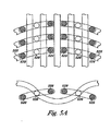
- Figure 5A is a representation of the positioning of a number of digit and cell contacts from an overhead perspective of the embodiment of the contact structure in Figure 4 after forming a trench structure.
- the representation illustrates cell contacts with hatch and digit contacts with no hatching.
- digit and cell contacts can be grouped into contact groups, for example, is the contacts share resources, such as source, drain and/or active regions.
- the contacts are grouped in groups 525 of three with each group having one digit contact 528 with a cell contact 529 on each side.
- Figure 5A illustrates six such groups arranged on the substrate.
- embodiments can have one or more contacts grouped together and can have one or more groups of contacts.
- the bottom portion illustrates an embodiment of the present disclosure in which a trench is formed through the at least one of the digit contacts of the substrate.
- the trench 527 is formed through two digit contacts 528.
- the trench is formed through all of the digit contacts on the substrate.
- Figure 5B is a cross-sectional view of an exemplary portion of the embodiment of the contact structure in Figure 4 after forming a trench structure.
- the trench 527 is formed in a filler material of a digit contact 528 between two insulative material structures 522.
- Figure 5B also shows a number of cell contacts 529.
- the trench structure can be formed in the filler material in a variety of manners. That is, as the reader will appreciate, the methods of the present disclosure can utilize a number of different techniques for patterning the different trenches, openings, layers, and other such formation described herein. These can include various deposition, planarization, etching, and/or erosion techniques, among others-
- the trench can be etched into the filler material.
- a damascene trench can formed.
- the filler material and the surrounding SOD material can be etched to form the trench.
- the depth of the trench (e.g., depth 523 of Figure 5B ) can be various depths. For example, a depth of 1500 A can be suitable in some structures.
- a spacer material can be applied to at least a portion of one of the side walls of the trench.
- Figure 5C is a cross-sectional view or an exemplary portion of the embodiment of the contact structure in Figure 4 after forming a trench structure if a sacrificial material is used.
- the trench 527 can be formed as above in a filler material of a digit contact 528 between two insulative material structures 522.
- Figure 5B also shows a number of cell contacts 529.
- a protective layer 521 can be provided over the sacrificial (e.g., cell structures 529) and insulative layers 522.
- the protective layer can, for example, be fabricated from Tetraethyl Orthosilicate, Si(OC 2 H 5 ) 4 , among other suitable materials.
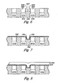
- Figure 6 provides a cross-sectional view of an exemplary portion of the embodiment of the contact structure in Figure 3B after applying a spacer material.
- a spacer material 630 is applied on each side wall of the trench 627.
- This spacer material can be any suitable spacer material.
- a dielectric material such as Tetramethyl Orthosilicate or Silicon Nitride, can be used as a spacer material.
- the spacer material can also be applied in a variety of thicknesses. For example, a thickness of 250 A of spacer material can be applied via chemical vapor deposition (CVD), among other deposition techniques.
- CVD chemical vapor deposition
- this material can be removed, for example, after spacer formation.
- Peripheral contracts can be patterned and plugs, interconnects, openings, and trenches can be filled with conductive material. In some embodiments, the filling of the plugs, interconnects, openings, and trenches can be done at the same time.
- Figure 7 is a cross-sectional view of an exemplary portion of the embodiment of the contact structure in Figure 6 after applying a liner material.
- the liner material can be deposited over the trench, the spacer material, and/or the top surface of the insulator and filler materials.
- the embodiment of Figure 7 illustrates a deposition over all of these surfaces including the spacer material 730 positioned in the trench formed in filler material 726.
- a liner material can be used in some embodiments, for example, to form a barrier layer, to adhere one layer to another (e.g., to act as a glue or adhesive), and/or as a low resistance interface layer.
- Figure 8 is a cross-sectional view of an exemplary portion of the embodiment of the contact structure in Figure 7 after applying a conductor material.
- a conductor material can be deposited over the liner material, including the portions positioned over the trench, the spacer material, and/or the top surface of the insulator and filler materials.
- the embodiment of Figure 8 illustrates a deposition of the conductor material 834 over a liner 832 covering all of these surfaces.
- a damascene conductor material can be deposited.
- Various embodiments utilize different thicknesses of such conductor materials.
- 75 A Titanium, 75 A Titanium Nitride, and/or 300 A Tungsten (W) can be applied, among other quantities and material types.
- Embodiments can include filling a number of open contacts with conductive material 834 during the process of depositing the conductive material 834 into the trench.
- the conductive material is a material selected from the group including. Titanium, Titanium Nitride, Tungsten Nitride. Tungsten, and a combination of at least two of the above materials.
- Titanium Nitride and Titanium/Titanium Nitride are two such combinations.
- Such materials can be used to fill the trench with the conductor material 834.
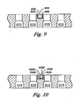
- Figure 9 is a cross-sectional view of an exemplary portion of the embodiment of the contact structure in Figure 8 after recessing the conductor material.
- the conductor material can be planarized in a variety of manners. If planarization is performed, a top oxide layer of the device can be eroded, for example such that the conductor material and the liner material positioned outside of the trench can be removed.
- this process can provide a trench structure having a conductor material 934, mounted in a liner 932, and having spacers 930 therein.
- the erosion can also remove a portion of the insulator and filler materials as the process erodes substantially all of the liner material positioned outside the trench.
- the insulator layer e.g., oxide material
- the insulator layer is eroded about 200 A in this process.
- Figure 10 is a cross-sectional view of an exemplary portion of the embodiment of the contact structure in Figure 9 after applying a cap material.
- the conductor material 1034 can be recessed, for example, to provide room within the trench for a cap.
- the conductor can be recessed to a depth of about 700 A, among other depths.
- the liner material 1032 may also be eroded between the spacer material 1030 and the conductor material 1034.
- a cap material 1036 can be deposited in the recess formed from the removal of the portion of the conductor material 1034 and, in some embodiments, the liner material 1032.
- a dielectric cap can be deposited over the trench conductor (e.g., Silicon Nitride or Silicon Oxide), to fill the trench.
- the cap material can be deposited in a thickness sufficient to cover the conductor material and, in some embodiments, liner material.
- the cap can be planarized. During this process, the insulator material and/or the filler material can also be eroded.
- the present disclosure includes a number of semiconductor structure embodiments.
- the semiconductor structure includes a trench structure having at least one side wall formed in an insulator material, and a spacer material positioned on the at least one side wall.
- This exemplary embodiment also includes a conductive material positioned within the trench structure and a cap material positioned over the conductive material.
- the trench structure can be a damascene trench structure.
- the trench structure can be formed along a path over a number of digit contacts and not over a number of cell contacts, in various embodiments. In some embodiments, the trench structure can be formed only over digit contacts.
- Embodiments can also include a liner material positioned within the trench structure and over at least a portion of the spacer material.
- the conductive material can be positioned in a contact opening formed over a number of the digit contacts, for example.
- the cap material can be positioned in the contact openings for over the number of the digit contacts.
- Various types of components can be formed in the active areas. Such components include imaging devices, memory devices or logic devices, among others.
- the present disclosure also includes a number of memory device embodiments.
- the memory device includes a semiconductor substrate including a number of contacts, a trench structure positioned over a number of the contacts, the trench structure having at least one side wall formed in an insulator material, a spacer material positioned on the at least one side wall, a conductive material positioned within the trench structure, and a cap material positioned over the conductive material.
- the integrated circuit includes a semiconductor substrate including a number of cell and digit contacts.
- a trench structure can be positioned over the digit contacts with the trench structure having at least one side wall formed in an insulator material.
- a spacer material can be positioned on the at least one side wall with a liner material positioned within the trench structure and over at least a portion of the spacer material, in some embodiments.
- a conductive material can be positioned within the trench structure and a cap material positioned over the conductive material.
- a completed integrated circuit can include an array of memory cells for a DRAM or other memory device.
- logic devices for gate arrays, microprocessors, and/or digital signal processors can be formed in the active regions.
- Figure 11 is a cross-sectional view of an exemplary integrated circuit that includes an embodiment of the contact structures of the present disclosure.
- the various structures illustrated can be formed using the techniques described above, among others.
- a stacked-cell DRAM 1140 includes a semiconductor substrate 1142 with multiple active regions 1144 separated by shallow trench isolation regions 1146.
- Doped regions 1152, 1153 can be formed, for example, by a diffusion implanted process with the regions 1152 serving as storage nodes for memory cells of the DRAM.
- Gates 1112, 1116, 1118, and 1120 arc provided in the integrated circuit.
- one or more of the gates can include nitride or other spacers provided on either side of the gates (not shown).
- Gates can include a polysilicon layer 1114 and a cap provided by an insulating material, for example.
- the insulating materials can include, for example, an oxide, a nitride, or a composite such as oxide/nitride or oxide/nitride/oxide combinations, among others.
- Gates can also include a barrier metal layer and a metal layer between the polysilicon layer 1114 and the cap.
- Suitable barrier metal layers include tungsten nitride, titanium nitride, and tantalum nitride, among others.
- the metal layer can include tungsten, tungsten silicide, titanium silicide, or cobalt silicide, among others.
- Polysilicon material components 1126 form the contacts to the drain and source regions 1152.
- capacitor cells comprise lower storage node electrodes 1162, a cell dielectric 1164, and an upper electrode 1166.
- a metal contact 1168 provides the electrical connection between a digit contact, formed according to an embodiment of the present disclosure, which serves as the bit line and a first metallization layer 1170.
- the contact includes spacer material 1130 provided within a trench formed between insulation material structures 1122, a liner 1132, a conductor material 1134, and a cap material 1136.
- An insulating layer 1172 can be used to separate the first metallization layer 1170 from a second metallization layer 1174.
- the semiconductor wafer can be covered by a passivation layer 1176.
- Figure 11 illustrates a stacked-cell DRAM
- contacts formed according to the techniques described above can be incorporated into any other type of memory such as trench cell DRAMs, flash memory, embedded memory, electrically erasable programmable read only memory (EEPROM), and the like.
- EEPROM electrically erasable programmable read only memory
- the present disclosure also includes a number of electronic system embodiments.
- the system includes a controller; and a memory device coupled to the controller, the memory device having an array of memory cells.
- Such memory can be a dynamic random access memory device or other such memory component.
- the controller can be a processor.
- Memory cells can include components such as a semiconductor substrate.
- the substrate can include a number of contacts, a contact structure forming at least one of the contacts.
- the contact structure can have at least one side wall formed in an insulator material and a spacer material positioned on the at least one side wall.
- the structure can also include a liner material positioned within the contact structure and over at least a portion of the spacer material, a conductive material positioned within the contact structure, and a cap material positioned over the conductive material.
- Figure 12 is an exemplary electronic system that can include embodiments of the contact structures of the present disclosure. Embodiments of the present disclosure can also include an electronic system that incorporates the contacts formed according to embodiments described herein.
- Figure 12 provides an embodiment of a processor based system 1280 that includes a memory having contacts formed according to the present disclosure for use in a memory device 1282 and controlled by controller 1292.
- the system 1280 may also include one or more input devices 1284, e.g., a keyboard, touch screen, transceiver, mouse, etc.
- the input devices can be connected to the computing unit 1286 to allow a user to input data, instructions, etc., to operate the computing unit 1286.
- One or more output devices 1288 connected to the computing unit 1286 may also be provided as part of the system 1280 to display or otherwise output data generated by the processor 1290. Examples of output devices include printers, video terminals, monitors, display units, etc.
Landscapes
- Engineering & Computer Science (AREA)
- Manufacturing & Machinery (AREA)
- Internal Circuitry In Semiconductor Integrated Circuit Devices (AREA)
- Manufacturing Of Electrical Connectors (AREA)
- Semiconductor Memories (AREA)
- Electrodes Of Semiconductors (AREA)
- Metal-Oxide And Bipolar Metal-Oxide Semiconductor Integrated Circuits (AREA)
Applications Claiming Priority (2)
| Application Number | Priority Date | Filing Date | Title |
|---|---|---|---|
| US11/363,661 US20070202677A1 (en) | 2006-02-27 | 2006-02-27 | Contact formation |
| EP07751342A EP1989734A2 (de) | 2006-02-27 | 2007-02-20 | Bildung von kontakten |
Related Parent Applications (1)
| Application Number | Title | Priority Date | Filing Date |
|---|---|---|---|
| EP07751342.2 Division | 2007-02-20 |
Publications (2)
| Publication Number | Publication Date |
|---|---|
| EP2194573A2 true EP2194573A2 (de) | 2010-06-09 |
| EP2194573A3 EP2194573A3 (de) | 2013-05-01 |
Family
ID=38284019
Family Applications (2)
| Application Number | Title | Priority Date | Filing Date |
|---|---|---|---|
| EP07751342A Withdrawn EP1989734A2 (de) | 2006-02-27 | 2007-02-20 | Bildung von kontakten |
| EP20100001798 Withdrawn EP2194573A3 (de) | 2006-02-27 | 2007-02-20 | Kontaktbildung |
Family Applications Before (1)
| Application Number | Title | Priority Date | Filing Date |
|---|---|---|---|
| EP07751342A Withdrawn EP1989734A2 (de) | 2006-02-27 | 2007-02-20 | Bildung von kontakten |
Country Status (8)
| Country | Link |
|---|---|
| US (4) | US20070202677A1 (de) |
| EP (2) | EP1989734A2 (de) |
| JP (1) | JP5403398B2 (de) |
| KR (1) | KR101082288B1 (de) |
| CN (1) | CN101390208B (de) |
| SG (1) | SG183588A1 (de) |
| TW (1) | TWI343093B (de) |
| WO (1) | WO2007098236A2 (de) |
Families Citing this family (9)
| Publication number | Priority date | Publication date | Assignee | Title |
|---|---|---|---|---|
| US20070202677A1 (en) * | 2006-02-27 | 2007-08-30 | Micron Technology, Inc. | Contact formation |
| JP5403862B2 (ja) * | 2006-11-28 | 2014-01-29 | チェイル インダストリーズ インコーポレイテッド | 微細金属パターンの製造方法 |
| JP2009176819A (ja) * | 2008-01-22 | 2009-08-06 | Elpida Memory Inc | 半導体装置及びその製造方法 |
| TWI419033B (zh) * | 2009-03-05 | 2013-12-11 | Elan Microelectronics Corp | Method for manufacturing two - layer circuit board structure for capacitive touch panel |
| US8241944B2 (en) | 2010-07-02 | 2012-08-14 | Micron Technology, Inc. | Resistive RAM devices and methods |
| US20160086956A1 (en) * | 2013-04-30 | 2016-03-24 | Ps5 Luxco S.A.R.L. | Semiconductor device and method for manufacturing semiconductor device |
| US10998228B2 (en) * | 2014-06-12 | 2021-05-04 | Taiwan Semiconductor Manufacturing Company, Ltd. | Self-aligned interconnect with protection layer |
| TWI825786B (zh) * | 2022-04-21 | 2023-12-11 | 南亞科技股份有限公司 | 具有不同間距之位元線接觸點的半導體元件 |
| US12245421B2 (en) | 2022-04-21 | 2025-03-04 | Nanya Technology Corporation | Semiconductor device with bit line contacts of different pitches |
Family Cites Families (34)
| Publication number | Priority date | Publication date | Assignee | Title |
|---|---|---|---|---|
| JP3146316B2 (ja) * | 1991-05-17 | 2001-03-12 | 日本テキサス・インスツルメンツ株式会社 | 半導体装置及びその製造方法 |
| US6531730B2 (en) * | 1993-08-10 | 2003-03-11 | Micron Technology, Inc. | Capacitor compatible with high dielectric constant materials having a low contact resistance layer and the method for forming same |
| US5420061A (en) * | 1993-08-13 | 1995-05-30 | Micron Semiconductor, Inc. | Method for improving latchup immunity in a dual-polysilicon gate process |
| JP2765478B2 (ja) * | 1994-03-30 | 1998-06-18 | 日本電気株式会社 | 半導体装置およびその製造方法 |
| JP3532325B2 (ja) * | 1995-07-21 | 2004-05-31 | 株式会社東芝 | 半導体記憶装置 |
| JPH09260600A (ja) | 1996-03-19 | 1997-10-03 | Sharp Corp | 半導体メモリ素子の製造方法 |
| JPH09293781A (ja) | 1996-04-26 | 1997-11-11 | Sony Corp | 半導体装置の製造方法 |
| US5759892A (en) * | 1996-09-24 | 1998-06-02 | Taiwan Semiconductor Manufacturing Company Ltd | Formation of self-aligned capacitor contact module in stacked cyclindrical dram cell |
| KR100256057B1 (ko) * | 1997-12-23 | 2000-05-01 | 윤종용 | 초미세 선폭의 비트라인 캡핑을 위한 반도체 소자 제조방법 |
| US6262450B1 (en) * | 1998-04-22 | 2001-07-17 | International Business Machines Corporation | DRAM stack capacitor with vias and conductive connection extending from above conductive lines to the substrate |
| US6174767B1 (en) * | 1998-05-11 | 2001-01-16 | Vanguard International Semiconductor Corporation | Method of fabrication of capacitor and bit-line at same level for 8F2 DRAM cell with minimum bit-line coupling noise |
| TW468276B (en) | 1998-06-17 | 2001-12-11 | United Microelectronics Corp | Self-aligned method for forming capacitor |
| JP2001007039A (ja) * | 1999-06-18 | 2001-01-12 | Hitachi Ltd | 半導体集積回路装置の製造方法 |
| US6255168B1 (en) | 1999-09-13 | 2001-07-03 | United Microelectronics Corp. | Method for manufacturing bit line and bit line contact |
| US6504210B1 (en) * | 2000-06-23 | 2003-01-07 | International Business Machines Corporation | Fully encapsulated damascene gates for Gigabit DRAMs |
| US6376353B1 (en) * | 2000-07-03 | 2002-04-23 | Chartered Semiconductor Manufacturing Ltd. | Aluminum and copper bimetallic bond pad scheme for copper damascene interconnects |
| JP2003100769A (ja) * | 2001-09-20 | 2003-04-04 | Nec Corp | 半導体装置およびその製造方法 |
| TW518719B (en) * | 2001-10-26 | 2003-01-21 | Promos Technologies Inc | Manufacturing method of contact plug |
| KR100481173B1 (ko) * | 2002-07-12 | 2005-04-07 | 삼성전자주식회사 | 다마신 비트라인공정을 이용한 반도체 메모리장치 및 그의제조방법 |
| KR100481177B1 (ko) * | 2002-08-21 | 2005-04-07 | 삼성전자주식회사 | 셀 패드 콘택의 저항을 감소시킨 반도체 장치 및 그제조방법 |
| US6696339B1 (en) * | 2002-08-21 | 2004-02-24 | Micron Technology, Inc. | Dual-damascene bit line structures for microelectronic devices and methods of fabricating microelectronic devices |
| US7138719B2 (en) * | 2002-08-29 | 2006-11-21 | Micron Technology, Inc. | Trench interconnect structure and formation method |
| US6730959B1 (en) * | 2002-10-30 | 2004-05-04 | Powerchip Semiconductor Corp. | Structure of flash memory device and fabrication method thereof |
| KR100476710B1 (ko) * | 2003-02-05 | 2005-03-16 | 매그나칩 반도체 유한회사 | 반도체 소자의 금속배선 형성방법 |
| KR100468784B1 (ko) * | 2003-02-14 | 2005-01-29 | 삼성전자주식회사 | 콘택으로부터 형성된 하드 마스크를 사용하는 다마신과정으로 배선을 형성하는 방법 |
| US7074717B2 (en) * | 2003-03-04 | 2006-07-11 | Micron Technology, Inc. | Damascene processes for forming conductive structures |
| US6921692B2 (en) * | 2003-07-07 | 2005-07-26 | Micron Technology, Inc. | Methods of forming memory circuitry |
| US7217647B2 (en) * | 2004-11-04 | 2007-05-15 | International Business Machines Corporation | Structure and method of making a semiconductor integrated circuit tolerant of mis-alignment of a metal contact pattern |
| US20060148168A1 (en) * | 2005-01-06 | 2006-07-06 | Sheng-Chin Li | Process for fabricating dynamic random access memory |
| US8125018B2 (en) * | 2005-01-12 | 2012-02-28 | Spansion Llc | Memory device having trapezoidal bitlines and method of fabricating same |
| US7723229B2 (en) * | 2005-04-22 | 2010-05-25 | Macronix International Co., Ltd. | Process of forming a self-aligned contact in a semiconductor device |
| US7214621B2 (en) * | 2005-05-18 | 2007-05-08 | Micron Technology, Inc. | Methods of forming devices associated with semiconductor constructions |
| US20070048951A1 (en) * | 2005-08-31 | 2007-03-01 | Hocine Boubekeur | Method for production of semiconductor memory devices |
| US20070202677A1 (en) * | 2006-02-27 | 2007-08-30 | Micron Technology, Inc. | Contact formation |
-
2006
- 2006-02-27 US US11/363,661 patent/US20070202677A1/en not_active Abandoned
-
2007
- 2007-02-20 EP EP07751342A patent/EP1989734A2/de not_active Withdrawn
- 2007-02-20 CN CN2007800068498A patent/CN101390208B/zh active Active
- 2007-02-20 KR KR1020087023686A patent/KR101082288B1/ko active Active
- 2007-02-20 JP JP2008556414A patent/JP5403398B2/ja active Active
- 2007-02-20 EP EP20100001798 patent/EP2194573A3/de not_active Withdrawn
- 2007-02-20 WO PCT/US2007/004573 patent/WO2007098236A2/en not_active Ceased
- 2007-02-20 SG SG2011012978A patent/SG183588A1/en unknown
- 2007-02-26 TW TW096106457A patent/TWI343093B/zh active
-
2009
- 2009-03-11 US US12/401,996 patent/US7737022B2/en not_active Expired - Lifetime
-
2010
- 2010-05-26 US US12/787,684 patent/US8034706B2/en not_active Expired - Lifetime
-
2011
- 2011-09-20 US US13/237,126 patent/US8377819B2/en not_active Expired - Lifetime
Non-Patent Citations (1)
| Title |
|---|
| None |
Also Published As
| Publication number | Publication date |
|---|---|
| US8034706B2 (en) | 2011-10-11 |
| SG183588A1 (en) | 2012-09-27 |
| JP2009528678A (ja) | 2009-08-06 |
| US20070202677A1 (en) | 2007-08-30 |
| WO2007098236A2 (en) | 2007-08-30 |
| CN101390208B (zh) | 2012-06-13 |
| US20100233875A1 (en) | 2010-09-16 |
| EP2194573A3 (de) | 2013-05-01 |
| EP1989734A2 (de) | 2008-11-12 |
| JP5403398B2 (ja) | 2014-01-29 |
| KR20090003276A (ko) | 2009-01-09 |
| US20120009779A1 (en) | 2012-01-12 |
| US8377819B2 (en) | 2013-02-19 |
| CN101390208A (zh) | 2009-03-18 |
| TWI343093B (en) | 2011-06-01 |
| KR101082288B1 (ko) | 2011-11-09 |
| US7737022B2 (en) | 2010-06-15 |
| WO2007098236A3 (en) | 2007-11-22 |
| TW200739812A (en) | 2007-10-16 |
| US20090176365A1 (en) | 2009-07-09 |
Similar Documents
| Publication | Publication Date | Title |
|---|---|---|
| US8377819B2 (en) | Contact formation | |
| KR960005251B1 (ko) | 반도체 메모리장치의 제조방법 | |
| RU2176423C2 (ru) | Способ изготовления полупроводникового устройства | |
| US6727542B2 (en) | Semiconductor memory device and method for manufacturing the same | |
| JP2009528678A5 (de) | ||
| KR100335778B1 (ko) | 반도체 소자 및 그 제조 방법 | |
| US5665626A (en) | Method of making a chimney capacitor | |
| US6271099B1 (en) | Method for forming a capacitor of a DRAM cell | |
| EP4044232A1 (de) | Speicher und herstellungsverfahren dafür | |
| CN113517273B (zh) | 电容器阵列结构及其制备方法和半导体存储器件 | |
| KR100400327B1 (ko) | 반도체소자의 캐패시터 형성방법 | |
| KR100843940B1 (ko) | 반도체소자의 캐패시터 형성방법 | |
| CN120857485A (zh) | 存储器元件及其制造方法 | |
| US6400022B1 (en) | Semiconductor device and fabrication process therefor and capacitor structure | |
| US6855600B2 (en) | Method for manufacturing capacitor | |
| KR100929293B1 (ko) | 반도체 소자의 커패시터 제조 방법 | |
| KR100463242B1 (ko) | 반도체 소자의 캐패시터 형성방법 | |
| KR100609558B1 (ko) | 반도체소자의 캐패시터 제조방법 | |
| JP2004039683A (ja) | 半導体集積回路装置の製造方法および半導体集積回路装置 | |
| KR20010061027A (ko) | 반도체 소자의 캐패시터 하부전극 형성방법 | |
| KR20070122318A (ko) | 반도체 메모리 소자 및 그 형성방법 | |
| KR20050067553A (ko) | 강유전체 메모리 소자의 제조 방법 |
Legal Events
| Date | Code | Title | Description |
|---|---|---|---|
| PUAI | Public reference made under article 153(3) epc to a published international application that has entered the european phase |
Free format text: ORIGINAL CODE: 0009012 |
|
| AC | Divisional application: reference to earlier application |
Ref document number: 1989734 Country of ref document: EP Kind code of ref document: P |
|
| AK | Designated contracting states |
Kind code of ref document: A2 Designated state(s): AT BE BG CH CY CZ DE DK EE ES FI FR GB GR HU IE IS IT LI LT LU LV MC NL PL PT RO SE SI SK TR |
|
| AX | Request for extension of the european patent |
Extension state: AL BA HR MK RS |
|
| PUAL | Search report despatched |
Free format text: ORIGINAL CODE: 0009013 |
|
| AK | Designated contracting states |
Kind code of ref document: A3 Designated state(s): AT BE BG CH CY CZ DE DK EE ES FI FR GB GR HU IE IS IT LI LT LU LV MC NL PL PT RO SE SI SK TR |
|
| AX | Request for extension of the european patent |
Extension state: AL BA HR MK RS |
|
| RIC1 | Information provided on ipc code assigned before grant |
Ipc: H01L 27/108 20060101ALI20130326BHEP Ipc: H01L 21/768 20060101AFI20130326BHEP |
|
| 17P | Request for examination filed |
Effective date: 20131014 |
|
| 17Q | First examination report despatched |
Effective date: 20131204 |
|
| RIC1 | Information provided on ipc code assigned before grant |
Ipc: H01L 21/768 20060101AFI20150312BHEP Ipc: H01L 27/108 20060101ALI20150312BHEP Ipc: H01L 27/02 20060101ALI20150312BHEP |
|
| GRAJ | Information related to disapproval of communication of intention to grant by the applicant or resumption of examination proceedings by the epo deleted |
Free format text: ORIGINAL CODE: EPIDOSDIGR1 |
|
| GRAP | Despatch of communication of intention to grant a patent |
Free format text: ORIGINAL CODE: EPIDOSNIGR1 |
|
| RIC1 | Information provided on ipc code assigned before grant |
Ipc: H01L 21/768 20060101AFI20150324BHEP Ipc: H01L 27/108 20060101ALI20150324BHEP Ipc: H01L 27/02 20060101ALN20150324BHEP |
|
| GRAP | Despatch of communication of intention to grant a patent |
Free format text: ORIGINAL CODE: EPIDOSNIGR1 |
|
| INTG | Intention to grant announced |
Effective date: 20150508 |
|
| STAA | Information on the status of an ep patent application or granted ep patent |
Free format text: STATUS: THE APPLICATION HAS BEEN WITHDRAWN |
|
| 18W | Application withdrawn |
Effective date: 20150626 |