EP2194585B1 - Dispositif électroluminescent semi-conducteur - Google Patents
Dispositif électroluminescent semi-conducteur Download PDFInfo
- Publication number
- EP2194585B1 EP2194585B1 EP09013441.2A EP09013441A EP2194585B1 EP 2194585 B1 EP2194585 B1 EP 2194585B1 EP 09013441 A EP09013441 A EP 09013441A EP 2194585 B1 EP2194585 B1 EP 2194585B1
- Authority
- EP
- European Patent Office
- Prior art keywords
- layer
- light emitting
- conductive
- emitting device
- semiconductor light
- Prior art date
- Legal status (The legal status is an assumption and is not a legal conclusion. Google has not performed a legal analysis and makes no representation as to the accuracy of the status listed.)
- Not-in-force
Links
Images



Classifications
-
- H—ELECTRICITY
- H10—SEMICONDUCTOR DEVICES; ELECTRIC SOLID-STATE DEVICES NOT OTHERWISE PROVIDED FOR
- H10H—INORGANIC LIGHT-EMITTING SEMICONDUCTOR DEVICES HAVING POTENTIAL BARRIERS
- H10H20/00—Individual inorganic light-emitting semiconductor devices having potential barriers, e.g. light-emitting diodes [LED]
- H10H20/80—Constructional details
- H10H20/83—Electrodes
- H10H20/831—Electrodes characterised by their shape
-
- H—ELECTRICITY
- H10—SEMICONDUCTOR DEVICES; ELECTRIC SOLID-STATE DEVICES NOT OTHERWISE PROVIDED FOR
- H10H—INORGANIC LIGHT-EMITTING SEMICONDUCTOR DEVICES HAVING POTENTIAL BARRIERS
- H10H20/00—Individual inorganic light-emitting semiconductor devices having potential barriers, e.g. light-emitting diodes [LED]
- H10H20/80—Constructional details
- H10H20/84—Coatings, e.g. passivation layers or antireflective coatings
-
- H—ELECTRICITY
- H10—SEMICONDUCTOR DEVICES; ELECTRIC SOLID-STATE DEVICES NOT OTHERWISE PROVIDED FOR
- H10H—INORGANIC LIGHT-EMITTING SEMICONDUCTOR DEVICES HAVING POTENTIAL BARRIERS
- H10H20/00—Individual inorganic light-emitting semiconductor devices having potential barriers, e.g. light-emitting diodes [LED]
- H10H20/01—Manufacture or treatment
- H10H20/011—Manufacture or treatment of bodies, e.g. forming semiconductor layers
- H10H20/018—Bonding of wafers
-
- H—ELECTRICITY
- H10—SEMICONDUCTOR DEVICES; ELECTRIC SOLID-STATE DEVICES NOT OTHERWISE PROVIDED FOR
- H10H—INORGANIC LIGHT-EMITTING SEMICONDUCTOR DEVICES HAVING POTENTIAL BARRIERS
- H10H20/00—Individual inorganic light-emitting semiconductor devices having potential barriers, e.g. light-emitting diodes [LED]
- H10H20/01—Manufacture or treatment
- H10H20/032—Manufacture or treatment of electrodes
Definitions
- the invention as claimed in claim 1 relates to a semiconductor light emitting device.
- Groups III-V nitride semiconductors have been variously applied to an optical device such as blue and green light emitting diodes (LED), a high speed switching device, such as a MOSFET (Metal Semiconductor Field Effect Transistor) and an HEMT (Hetero junction Field Effect Transistors), and a light source of a lighting device or a display device.
- LED blue and green light emitting diodes
- MOSFET Metal Semiconductor Field Effect Transistor
- HEMT Hetero junction Field Effect Transistors
- the nitride semiconductor is mainly used for the LED or an LD (laser diode), and studies have been continuously conducted to improve the manufacturing process or light efficiency of the nitride semiconductor.
- the claimed invention provides a semiconductor light emitting device capable of separating a chip without performing an isolation etching process.
- the claimed invention provides a semiconductor light emitting device capable of preventing interlayer short from occurring in an outer wall of a light emitting structure.
- the claimed invention provides a semiconductor light emitting device as defined in claim 1.
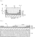
- FIG. 1 is a side sectional view showing a semiconductor light emitting device according to an embodiment.
- the semiconductor light emitting device 100 comprises a light emitting structure 135, an electrode 181, a conductive layer 140, an insulating layer 145, an electrode layer 150 and a conductive support member 160.
- the semiconductor light emitting device 100 comprises a compound semiconductor, e.g., an LED (light emitting diode) based on III-V group compound semiconductors, and the LED may comprise a color LED emitting blue light, green light or red light or an UV (ultra violet) LED.
- the light emitted from the LED may be variously realized within the technical scope of the embodiment.
- the light emitting structure 135 comprises a first conductivity semiconductor layer (hereinafter also referred to as “first conductive semiconductor layer”) 110, an active layer 120 and a second conductivity semiconductor layer (hereinafter also referred to as “second conductive semiconductor layer”).
- the first conductive semiconductor layer 110 may comprise one selected from the group consisting of GaN, AlN, AlGaN, InGaN, InN, InAlGaN, AlInN, AlGaAs, GaP, GaAs, GaAsP and AlGaInP, which are compound semiconductors of III-V group elements doped with a first conductive dopant.
- the first conductive dopant comprises an N type dopant such as Si, Ge, Sn, Se or Te.
- the first conductive semiconductor layer 110 may have a single layer or a multilayer. However, the embodiment is not limited thereto.
- An electrode 181 is formed under the first conductive semiconductor layer 110, and can be provided in a predetermined pattern.
- the first conductive semiconductor layer 110 may be provided on a lower surface thereof with a roughness pattern.
- the active layer 120 is formed on the first conductive semiconductor layer 110 and may have a single quantum well structure or a multi-quantum well structure.
- the active layer 120 may have a period of a well layer and a barrier layer using compound semiconductor materials of the III-V group elements.
- the active layer 120 may have a period of an InGaN well layer and a GaN barrier layer.
- a conductive clad layer may be formed on and/or under the active layer 12, and may comprise an GaN-based layer.
- the second conductive semiconductor layer 130 is formed on the active layer 120, and may comprise one selected from the group consisting of GaN, AlN, AlGaN, InGaN, InN, InAlGaN, AlInN, AlGaAs, GaP, GaAs, GaAsP and AlGaInP, which are the compound semiconductors of III-V group elements doped with a second conductive dopant.
- the second conductive semiconductor layer 120 is a P type semiconductor layer
- the second conductive dopant comprises a P type dopant such as Mg and Zn.
- the second conductive semiconductor layer 120 may have a single layer or a multilayer. However, the embodiment is not limited thereto.
- the light emitting structure 135 may comprise an N type semiconductor layer or a P type semiconductor layer on the second conductive semiconductor layer 120. Further, the first conductive semiconductor layer 110 may be provided as a P type semiconductor layer and the second conductive semiconductor layer 130 may be provided as an N type semiconductor layer.
- the light emitting structure 135 may comprise at least one of an N-P junction structure, a P-N junction structure, an N-P-N junction structure and a P-N-P junction structure.
- the conductive layer 140 is formed at circumference of an upper portion of the light emitting structure 135.
- the conductive layer 140 and the electrode layer 150 are formed on the second conductive semiconductor layer 130.
- the conductive layer 140 is formed along the peripheral portion of an upper surface of the second conductive semiconductor layer 130 in the form of a band shape, a ring shape or a frame shape.
- the conductive layer 140 comprises transparent conductive material.
- the conductive layer 140 may comprise at least one selected from the group consisting of indium tin oxide (ITO), indium zinc oxide (IZO), indium zinc tin oxide (IZTO), indium aluminum zinc oxide (IAZO), indium gallium zinc oxide (IGZO), indium gallium tin oxide (IGTO), aluminum zinc oxide (AZO), antimony tin oxide (ATO), gallium zinc oxide (GZO), IrOx, RuOx, RuOx/ITO, Ni/IrOx/Au and Ni/IrOx/Au/ITO.
- the conductive layer 140 may have a thickness of about 0.02 ⁇ m to about 2 ⁇ m, and the thickness of the conductive layer 140 can be modified within the technical scope of the embodiment.
- the electrode layer 150 is formed at an inner side of an upper surface of the second conductive semiconductor layer 130 and is used to supply power of a second polarity.
- An outer peripheral portion of the electrode layer 150 may be formed on the conductive layer 140.
- the embodiment is not limited thereto.
- the electrode layer 150 may comprise at least one of an ohmic contact layer, a reflective layer, and an adhesive layer.
- the ohmic contact layer may be formed in the form of a layer or a plurality of patterns.
- the ohmic contact layer may be comprised at least one of a metal material and an oxide material.
- the ohmic contact layer may comprise at least one selected from the group consisting of ITO, IZO, IZTO, IAZO, IGZO, IGTO, AZO, ATO, GZO, IrOx, RuOx, RuOx/ITO, Ni/IrOx/Au, Ni/IrOx/Au/ITO, Pt, Ni, Au, Rh and Pd .
- the ohmic contact layer may have a thickness of about 10 ⁇ to about 1 ⁇ m. However, the embodiment is not limited thereto.
- the reflective layer may be formed at least one of layers and formed of at least one of Ag, Ni, Al, Rh, Pd, Ir, Ru, Mg, Zn, Pt, Au and Hf, and materials consisting of the selective combination of these elements.
- the adhesive layer may be formed at least one of layers and formed of at least one of Ti, Au, Sn, Ni, Cr, Ga, In, Bi, Cu, Ag, and Ta, and materials consisting of the selective combination of these elements.
- the electrode layer 150 may be used as a seed layer for a plating process.
- the seed layer may be formed at least one of Ti, Cr, Ta, Cr/Au, Cr/Cu, Ti/Au, Ta/Cu, and Ta/Ti/Cu.
- the insulating layer 145 is formed along the peripheral portion of an upper surface of the conductive layer 140.
- the insulating layer 145 may have a band shape, a ring shape or a frame shape. Further, the insulating layer 145 can be continuously formed like a closed loop or can be discontinuously formed.
- the insulating layer 145 may comprise one selected from the group consisting of SiO 2 , Si 3 N 4 , SiO x , SiN x , Al 2 O 3 and TiO 2 .
- the insulating layer 145 may have a thickness T1 or height of about 10 ⁇ m to about 100 ⁇ m, and may have a width W1 of about 10 ⁇ m to about 20 ⁇ m.
- the thickness T1 of the insulating layer 145 is equal to or larger than the thickness of the electrode layer 150 and is smaller than the thickness T2 of the conductive support member 160.
- the width W1 of the insulating layer 145 is equal to or less than the width of the conductive layer 140.
- the insulating layer 145 must have a thickness of at least 10 ⁇ m to prevent debris, which is generated from the conductive support member 160 when an abnormal impact is applied to the conductive support member 160 during a laser scribing process, from moving toward an outer wall of the light emitting structure 135.
- the insulating layer 145 has the width enough to stably maintain the adhesion state of the insulating layer.
- the conductive support member 160 is formed on the electrode layer 150.
- the conductive support member 160 may function as a base substrate of a chip and is used to supply power of a second polarity.
- the electrode layer 150 and/or the conductive support member 160 can be provided as a layer or a plurality of patterns.
- the conductive support member 160 may comprise Cu, Au, Ni, Mo, Cu-W, and carrier wafer such as Si, Ge, GaAs, ZnO, SiC, SiGe, and GaN.
- the conductive support member 160 may be formed through an electrolytic plating scheme or can be prepared in the form of a sheet. However, the embodiment is not limited thereto.
- the conductive support member 160 may have the thickness T2 of about 30 ⁇ m to about 150 ⁇ m. However, the embodiment is not limited thereto.
- the insulating layer 145 is disposed along the lower peripheral portion of the conductive support member 160.
- the insulating layer 145 may be disposed at both or all sides of the conductive support member 160.
- An extension line L1 of an outer surface of the insulating layer 145 and an extension line L2 of an outer surface of the conductive support member 160 can be disposed on the same line or the extension line L1 can be disposed outwardly from the extension line L2.
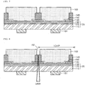
- FIGS. 2 to 9 are sectional views showing the procedure of manufacturing the semiconductor light emitting device according to the embodiment.
- a substrate 101 is loaded on growing equipment and a compound semiconductor layer of II to VI group elements is formed on the substrate 101.
- the growing equipment may comprise E-beam deposition equipment, physical vapor deposition (PVD) equipment, chemical vapor deposition (CVD) equipment, plasma laser deposition (PLD) equipment, a dual-type thermal evaporator, sputtering equipment and metal organic chemical vapor deposition (MOCVD) equipment.
- PVD physical vapor deposition
- CVD chemical vapor deposition
- PLD plasma laser deposition
- MOCVD metal organic chemical vapor deposition
- the substrate 101 may comprise one selected from the group consisting of sapphire (Al 2 O 3 ), GaN, SiC, ZnO, Si, GaP, InP, Ga 2 O 3 , a conductive substrate and GaAs.
- the substrate 101 may be provided thereof with a concave-convex pattern.
- a layer or a pattern using compound semiconductor of II to VI group elements may be formed on the substrate 101.
- at least one of a ZnO layer (not shown), a buffer layer (not shown) and an undoped semiconductor layer (not shown) may be formed on the substrate 101.
- the buffer layer and the undoped semiconductor layer may comprise the compound semiconductors of the III-V group elements.
- the buffer layer reduces a lattice constant difference from the substrate 101, and the undoped semiconductor layer may comprise an undoped GaN-based semiconductor layer.
- the light emitting structure 135 comprising the compound semiconductor layers is formed on the substrate 101.
- the first conductive semiconductor layer 110 is formed on the substrate 101
- the active layer 120 is formed on the first conductive semiconductor layer 110
- the second conductive semiconductor layer 130 is formed on the active layer 120.
- the first conductive semiconductor layer 110 may comprise one selected from the group consisting of GaN, AlN, AlGaN, InGaN, InN, InAlGaN, AlInN, AlGaAs, GaP, GaAs, GaAsP and AlGaInP, which are compound semiconductors of III-V group elements doped with the first conductive dopant.
- the first conductive dopant comprises the N type dopant such as Si, Ge, Sn, Se or Te.
- the first conductive semiconductor layer 110 may have the single layer or the multilayer. However, the embodiment is not limited thereto.
- the active layer 120 is formed on the first conductive semiconductor layer 110 and may have the single quantum well structure or the multi-quantum well structure.
- the active layer 120 may have an arrangement of the well layer and the barrier layer using the compound semiconductor materials of the III-V group elements.
- the active layer 120 may have an arrangement of the InGaN well layer and the GaN barrier layer.
- the conductive clad layer may be formed on and/or under the active layer 120, and may comprise the GaN-based layer.
- the second conductive semiconductor layer 130 is formed on the active layer 120, and may comprise one selected from the group consisting of GaN, AlN, AlGaN, InGaN, InN, InAlGaN, AlInN, AlGaAs, GaP, GaAs, GaAsP and AlGaInP, which are the compound semiconductors of the III-V group elements doped with the second conductive dopant.
- the second conductive semiconductor layer 120 is the P type semiconductor layer
- the second conductive dopant comprises the P type dopant such as Mg and Zn.
- the second conductive semiconductor layer 120 may have the single layer or the multilayer. However, the embodiment is not limited thereto.
- the first conductive semiconductor layer 110, the active layer 120, and the second conductive semiconductor layer 130 form the light emitting structure 135.
- a third conductivity semiconductor layer (hereinafter also “third conductive semiconductor layer”), e.g., an N type semiconductor layer or a P type semiconductor layer, may be formed on the second conductive semiconductor layer 130.
- the light emitting structure 135 may comprise at least one of the N-P junction structure, the P-N junction structure, the N-P-N junction structure and the P-N-P junction structure.
- the conductive layer 140 may be formed on the second conductive semiconductor layer 130 or the third conductive semiconductor layer.
- the conductive layer 140 is disposed along the peripheral portion of the upper surface of the second conductive semiconductor layer 130.
- the conductive layer 140 having a band shape, a ring shape or a frame shape may be formed along the peripheral surface of an inner area 141 of each chip on the second conductive semiconductor layer 130.
- the conductive layer 140 can be continuously formed or can be prepared in the shape of a closed loop.
- the conductive layer 140 is a transparent conductive material.
- the conductive layer 140 may comprise at least one selected from the group consisting of ITO, IZO, IZTO, IAZO, IGZO, IGTO, AZO, ATO, GZO, IrOx, RuOx, RuOx/ITO, Ni/IrOx/Au and Ni/IrOx/Au/ITO.
- the conductive layer 140 may have the thickness of about 0.02 ⁇ m to about 2 ⁇ m.
- the conductive layer 140 may be used as the seed layer for the plating process.
- the insulating layer 145 is formed on the conductive layer 140.
- the insulating layer 145 is disposed along the peripheral portion of the upper surface of the conductive layer 140 on the basis of an individual chip.
- the insulating layer 145 may have a band shape, a ring shape or a frame shape. Further, the insulating layer 145 can be continuously formed like a closed loop or can be discontinuously formed. The insulating layer 145 can be disposed at both or all sides of the conductive layer 140 on the basis of four sides of the chip.
- the insulating layer 145 may comprise at least one selected from the group consisting of SiO 2 , SiO 3 N 4 , SiO x , SiN x , Al 2 O 3 and TiO 2 , which are transparent insulating materials.
- the insulating layer 145 may have the thickness T1 of about 10 ⁇ m to about 100 ⁇ m, and may have the width W1 of about 10 ⁇ m to about 20 ⁇ m.
- the width W1 of the insulating layer 145 is smaller than the width of the conductive layer 140.
- the electrode layer 150 is formed on the inner side of the upper surface of the second conductive semiconductor layer 130.
- An outer side of the electrode layer 150 is formed on the upper surface of the conductive layer 140.
- the electrode layer 150 may comprise material having ohmic and reflective characteristics and used as a seed layer.
- the electrode layer 150 may function as a reflective electrode layer and has a reflectivity of about 50% or more.
- the electrode layer 150 may comprise at least one of an ohmic contact layer, a reflective layer, and an adhesive layer.
- the ohmic contact layer may be formed in the form of a layer or a plurality of patterns.
- the ohmic contact layer may be comprised at least one of a metal material and an oxide material.
- the ohmic contact layer may comprise at least one selected from the group consisting of ITO, IZO, IZTO, IAZO, IGZO, IGTO, AZO, ATO, GZO, IrOx, RuOx, RuOx/ITO, Ni/IrOx/Au, Ni/IrOx/Au/ITO, Pt, Ni, Au, Rh and Pd .
- the ohmic contact layer may have a thickness of about 10 ⁇ to about 1 ⁇ m. However, the embodiment is not limited thereto.
- the reflective layer may be formed at least one of layers and formed of at least one of Ag, Ni, Al, Rh, Pd, Ir, Ru, Mg, Zn, Pt, Au and Hf, and materials consisting of the selective combination of these elements.
- the adhesive layer may be formed at least one of layers and formed of at least one of Ti, Au, Sn, Ni, Cr, Ga, In, Bi, Cu, Ag, and Ta, and materials consisting of the selective combination of these elements.
- the electrode layer 150 may be used as a seed layer for a plating process.
- the seed layer may be formed at least one of Ti, Cr, Ta, Cr/Au, Cr/Cu, Ti/Au, Ta/Cu, and Ta/Ti/Cu.
- the electrode layer 150 may function as a reflective electrode layer and has a reflectivity of about 50% or more.
- the electrode layer 150 may have a thickness equal to or less than the thickness of the insulating layer 145.
- the conductive support member 160 is formed on the electrode layer 150.
- the conductive support member 160 may have the predetermined thickness, e.g., about 30 ⁇ m to about 150 ⁇ m, and may function as the base substrate of the chip.
- the conductive support member 160 may comprise Cu, Au, Ni, Mo, Cu-W, and carrier wafer such as Si, Ge, GaAs, ZnO, SiC, SiGe and GaN.
- the conductive support member 160 may be formed through the electrolytic plating scheme or can be prepared in the form of the sheet. However, the embodiment is not limited thereto.
- the conductive support member 160 may be formed at the inner side of the insulating layer 145, or at the inner side and on the upper surface of the insulating layer 145. That is, the conductive support member 160 may be located at the inner side of the insulating layer 145 or on the insulating layer 145 according to the thickness of the conductive support member 160.
- the embodiment is not limited thereto.
- a boundary area 162 between chips may function as a gap at which the conductive support members 160 of adjacent chips are spaced apart from each other.
- the boundary area 162 can be a channel area.
- the extension line L1 of the outer surface of the insulating layer 145 is located outwardly from the extension line L2 of the outer surface of the conductive support member 160.
- the conductive support members 160 may be combined with each other.
- the substrate 101 is removed.
- the substrate 101 may be removed using a physical method and/or a chemical method.
- LLO laser lift off
- laser having a predetermined wavelength range is irradiated onto the substrate 101, so the substrate 101 is separated from the first conductive semiconductor layer 110.
- the chemical method when another semiconductor layer (e.g., a buffer layer) is formed between the substrate 101 and the first conductive semiconductor layer 110, the buffer layer is removed using wet etch solution, so the substrate 101 is separated from the first conductive semiconductor layer 110.
- another semiconductor layer e.g., a buffer layer
- the electrode 181 is formed under the first conductive semiconductor layer 110 of the light emitting structure 135 in a chip unit and is provided as a predetermined pattern.
- an electrode formation process is performed without performing an isolation etching process (e.g., ICP) relative to the boundary area (i.e. channel area) between chips of the light emitting structure 135, so that the chip manufacturing process can be improved.
- ICP isolation etching process
- the semiconductor light emitting device 100 is divided as a chip unit.
- laser is irradiated onto the boundary area between the chips using laser scribing equipment, so the chip boundary area is divided.
- chip separation is performed through a breaking process. Even if the conductive support members 160 have been combined with each other, the conductive support members 160 are broken and separated from each other due to pressing force during the breaking process.
- the laser can be irradiated up to the conductive layer 140. Since the conductive layer 140 is a transparent material such as ITO, no debris or fragments are generated when the laser passes through the conductive layer 140, so the interlayer short-circuit can be prevented from occurring in the outer wall of the light emitting structure 135.
- the conductive layer 140 is a transparent material such as ITO, no debris or fragments are generated when the laser passes through the conductive layer 140, so the interlayer short-circuit can be prevented from occurring in the outer wall of the light emitting structure 135.
- the insulating layer 145 can prevent the debris or fragments from moving toward the light emitting structure 135, so that the interlayer short-circuit can be prevented from occurring in the outer wall of the light emitting structure 135.
- the insulating layer 145 must have the thickness of at least 10 ⁇ m to prevent the debris or fragments, which are generated from the conductive support member 160 when the abnormal impact is applied to the conductive support member 160 during the laser scribing process, from moving toward the outer wall of the light emitting structure 135.
- the chips can be separated from each other without applying an impact to the conductive support member 160, so the side surfaces of the conductive support member 160 can be provided in a clean state.
- the embodiment can provide a semiconductor light emitting device such as an LED.
Landscapes
- Led Devices (AREA)
Claims (13)
- Dispositif électroluminescent semi-conducteur comprenant :une structure électroluminescente (135) comprenant une pluralité de couches semi-conductrices de composés (110, 120, 130) ;une couche d'électrode (150) sur la structure électroluminescente (135) ;un élément de support conducteur (160) sur la couche d'électrode (150) ;une couche conductrice (140) formée le long d'une partie périphérique de la surface supérieure de la structure électroluminescente (35) ; etune couche isolante (145) sur la couche conductrice (140) disposée le long de la partie périphérique de la surface supérieure de la structure électroluminescente (135),dans lequel la structure électroluminescente (135) comprend :une couche semi-conductrice d'un premier type de conductivité (110) ;une couche active (120) sur la couche conductrice du premier type de conductivité (110) ; etune couche semi-conductrice d'un deuxième type de conductivité (130) entre la couche active (120) et la couche d'électrode (150),dans lequel une partie de la couche conductrice (40) établit un contact avec la couche d'électrode (150),dans lequel la couche conductrice (140) est constituée d'un matériau transparent, et dans lequel l'épaisseur de la couche isolante (145) est égale ou supérieure à l'épaisseur de la couche d'électrode (150) et inférieure à l'épaisseur de l'élément de support conducteur (160).
- Dispositif électroluminescent semi-conducteur selon la revendication 1, dans lequel la couche conductrice (140) et la couche isolante (145) comprennent au moins une forme parmi une forme de bande, une forme de bague et une forme de cadre, et présentent une configuration continue.
- Dispositif électroluminescent semi-conducteur selon l'une quelconque des revendications 1-2, dans lequel un côté extérieur de la couche isolante (145) est situé à l'extérieur par rapport au côté de l'élément de support conducteur (160),
dans lequel la couche isolante (145) est disposée le long de la portion périphérique d'une surface supérieure de la couche conductrice (140). - Dispositif électroluminescent semi-conducteur selon l'une quelconque des revendications 1-3, dans lequel la couche d'électrode (150) comprend au moins une couche parmi une couche de contact ohmique, une couche réfléchissante, et une couche adhésive.
- Dispositif électroluminescent semi-conducteur selon l'une quelconque des revendications 1-4, comprenant une électrode (181) sous la structure électroluminescente (135).
- Dispositif électroluminescent semi-conducteur selon l'une quelconque des revendications 1-5, dans lequel la couche isolante (145) a une épaisseur d'au moins 10 µm, et
dans lequel la largeur de la couche isolante (145) est égale ou inférieure à la largeur de la couche conductrice (140). - Dispositif électroluminescent semi-conducteur selon l'une quelconque des revendications 1-6, dans lequel la couche conductrice (140) comprend un composant sélectionné parmi le groupe constitué d'oxyde d'indium-étain (ITO), oxyde d'indium-zinc (IZO), oxyde d'indium-zinc-étain (IZTO), oxyde d'indium-aluminium-zinc (IAZO), oxyde d'indium-gallium-zinc (IGZO), oxyde d'indium-gallium-étain (IGTO), oxyde d'aluminium-zinc (AZO), oxyde d'antimoine-étain (ATO), oxyde de gallium-étain (GZO), IrOX, TuOx, RuOx/ITO, Ni/IrOx/Au, et Ni/IrOx/Au/ITO.
- Dispositif électroluminescent semi-conducteur selon l'une quelconque des revendications 1-7, dans lequel une partie périphérique extérieure de la couche d'électrode (150) est formée sur la couche conductrice (140).
- Dispositif électroluminescent semi-conducteur selon l'une quelconque des revendications 1-8, dans lequel l'élément de support conducteur (160) est formé sur un côté intérieur et sur la surface supérieure de la couche isolante (145).
- Dispositif électroluminescent semi-conducteur selon l'une quelconque des revendications 1-9, dans lequel la couche conductrice (140) et la couche d'électrode (150) comprennent au moins un composant sélectionné parmi le groupe constitué d'oxyde d'indium-étain (ITO), oxyde d'indium-zinc (IZO), oxyde d'indium-zinc-étain (IZTO), oxyde d'indium-aluminium-zinc (IAZO), oxyde d'indium-gallium-zinc (IGZO), oxyde d'indium-gallium-étain (IGTO), oxyde d'aluminium-zinc (AZO), oxyde d'antimoine-étain (ATO), oxyde de gallium-étain (GZO), IrOX, TuOx, RuOx/ITO, Ni/IrOx/Au, et Ni/IrOx/Au/ITO, et la couche isolante (145) comprend au moins un composant sélectionné parmi le groupe constitué de SiO2, Si3N4, TiO2 et Al2O3,
dans lequel l'élément de support conducteur (160) comprend un composant parmi le Cu, l'Au, le Ni, le Mo, ou le CuW. - Dispositif électroluminescent semi-conducteur selon l'une quelconque des revendications 1-10, dans lequel la couche isolante (145) est alignée sur un plan différent de la surface supérieure de l'élément de support conducteur (160).
- Dispositif électroluminescent semi-conducteur selon l'une quelconque des revendications 1-11, dans lequel la couche isolante (145) a une épaisseur comprise entre 10 µm et 100 µm,
dans lequel l'élément de support conducteur (160) a une épaisseur comprise entre 30 µm et 150 µm,
dans lequel la couche conductrice (140) a une épaisseur comprise entre 0,02 µm et 2 µm. - Dispositif électroluminescent semi-conducteur selon l'une quelconque des revendications 1-12, dans lequel la structure électroluminescente (135) comprend une couche semi-conductrice de type N ou une couche semi-conductrice de type P sur la couche semi-conductrice du deuxième type de conductivité (130).
Applications Claiming Priority (1)
| Application Number | Priority Date | Filing Date | Title |
|---|---|---|---|
| KR1020080105258A KR100962899B1 (ko) | 2008-10-27 | 2008-10-27 | 반도체 발광소자 및 그 제조방법 |
Publications (2)
| Publication Number | Publication Date |
|---|---|
| EP2194585A1 EP2194585A1 (fr) | 2010-06-09 |
| EP2194585B1 true EP2194585B1 (fr) | 2018-12-05 |
Family
ID=42026224
Family Applications (1)
| Application Number | Title | Priority Date | Filing Date |
|---|---|---|---|
| EP09013441.2A Not-in-force EP2194585B1 (fr) | 2008-10-27 | 2009-10-23 | Dispositif électroluminescent semi-conducteur |
Country Status (4)
| Country | Link |
|---|---|
| US (2) | US20100102350A1 (fr) |
| EP (1) | EP2194585B1 (fr) |
| KR (1) | KR100962899B1 (fr) |
| CN (1) | CN101728471B (fr) |
Families Citing this family (12)
| Publication number | Priority date | Publication date | Assignee | Title |
|---|---|---|---|---|
| JP4702442B2 (ja) * | 2008-12-12 | 2011-06-15 | ソニー株式会社 | 半導体発光素子及びその製造方法 |
| KR101064091B1 (ko) * | 2009-02-23 | 2011-09-08 | 엘지이노텍 주식회사 | 반도체 발광소자 및 그 제조방법 |
| KR101020945B1 (ko) | 2009-12-21 | 2011-03-09 | 엘지이노텍 주식회사 | 발광 소자, 발광 소자 패키지 및 발광 소자 제조방법 |
| KR101039946B1 (ko) * | 2009-12-21 | 2011-06-09 | 엘지이노텍 주식회사 | 발광 소자, 발광 소자 패키지 및 발광 소자 제조방법 |
| KR101064049B1 (ko) | 2010-02-18 | 2011-09-08 | 엘지이노텍 주식회사 | 반도체 발광소자 및 그 제조방법, 발광소자 패키지 |
| KR101020963B1 (ko) | 2010-04-23 | 2011-03-09 | 엘지이노텍 주식회사 | 발광 소자, 발광 소자 제조방법 및 발광 소자 패키지 |
| CN102214649B (zh) * | 2011-05-25 | 2013-03-13 | 映瑞光电科技(上海)有限公司 | 一种led封装结构及其制备方法 |
| EP2816621A4 (fr) * | 2012-02-15 | 2015-10-21 | Panasonic Ip Man Co Ltd | Appareil électroluminescent et son procédé de fabrication |
| CN102779911A (zh) * | 2012-04-09 | 2012-11-14 | 厦门市三安光电科技有限公司 | 一种垂直结构氮化镓基发光元件的制作方法 |
| KR101886156B1 (ko) * | 2012-08-21 | 2018-09-11 | 엘지이노텍 주식회사 | 발광소자 |
| KR102302592B1 (ko) * | 2017-07-18 | 2021-09-15 | 삼성전자주식회사 | 반도체 발광 소자 |
| CN116569345A (zh) * | 2020-11-27 | 2023-08-08 | 苏州晶湛半导体有限公司 | GaN基激光器及其制作方法 |
Family Cites Families (15)
| Publication number | Priority date | Publication date | Assignee | Title |
|---|---|---|---|---|
| KR100506740B1 (ko) * | 2003-12-23 | 2005-08-08 | 삼성전기주식회사 | 질화물 반도체 발광소자 및 그 제조방법 |
| KR20060125079A (ko) | 2005-06-01 | 2006-12-06 | 삼성전기주식회사 | 수직구조 질화갈륨계 발광다이오드 소자 및 그 제조방법 |
| SG130975A1 (en) * | 2005-09-29 | 2007-04-26 | Tinggi Tech Private Ltd | Fabrication of semiconductor devices for light emission |
| KR20070044099A (ko) | 2005-10-24 | 2007-04-27 | 김성진 | 질화물 반도체 발광 다이오드 및 그 제조방법 |
| KR100640496B1 (ko) * | 2005-11-23 | 2006-11-01 | 삼성전기주식회사 | 수직구조 질화갈륨계 발광다이오드 소자 |
| KR101154666B1 (ko) | 2006-01-03 | 2012-06-08 | 엘지이노텍 주식회사 | 수직형 발광소자 및 그 제조방법 |
| US7928462B2 (en) * | 2006-02-16 | 2011-04-19 | Lg Electronics Inc. | Light emitting device having vertical structure, package thereof and method for manufacturing the same |
| US7696523B2 (en) * | 2006-03-14 | 2010-04-13 | Lg Electronics Inc. | Light emitting device having vertical structure and method for manufacturing the same |
| KR100774196B1 (ko) | 2006-03-14 | 2007-11-08 | 엘지전자 주식회사 | 수직형 발광 소자 제조방법 |
| WO2007148866A1 (fr) * | 2006-06-23 | 2007-12-27 | Lg Electronics Inc. | Diode électroluminescente ayant une topologie verticale et son procédé de fabrication |
| JP5148079B2 (ja) | 2006-07-25 | 2013-02-20 | 富士通株式会社 | 液冷ユニット用熱交換器および液冷ユニット並びに電子機器 |
| KR100867541B1 (ko) * | 2006-11-14 | 2008-11-06 | 삼성전기주식회사 | 수직형 발광 소자의 제조 방법 |
| JP2008186959A (ja) * | 2007-01-29 | 2008-08-14 | Toyoda Gosei Co Ltd | Iii−v族半導体素子、およびその製造方法 |
| KR100878326B1 (ko) | 2007-07-03 | 2009-01-14 | 한국광기술원 | 칩스케일 패키징 발광소자 및 그의 제조방법 |
| KR100907223B1 (ko) | 2007-07-03 | 2009-07-10 | 한국광기술원 | 수직형 발광 다이오드 및 그의 제조방법 |
-
2008
- 2008-10-27 KR KR1020080105258A patent/KR100962899B1/ko active Active
-
2009
- 2009-10-23 EP EP09013441.2A patent/EP2194585B1/fr not_active Not-in-force
- 2009-10-27 CN CN2009102070493A patent/CN101728471B/zh not_active Expired - Fee Related
- 2009-10-27 US US12/606,590 patent/US20100102350A1/en not_active Abandoned
-
2011
- 2011-07-06 US US13/177,406 patent/US8471286B2/en active Active
Non-Patent Citations (1)
| Title |
|---|
| None * |
Also Published As
| Publication number | Publication date |
|---|---|
| US20110260207A1 (en) | 2011-10-27 |
| US8471286B2 (en) | 2013-06-25 |
| CN101728471A (zh) | 2010-06-09 |
| KR100962899B1 (ko) | 2010-06-10 |
| KR20100046425A (ko) | 2010-05-07 |
| EP2194585A1 (fr) | 2010-06-09 |
| US20100102350A1 (en) | 2010-04-29 |
| CN101728471B (zh) | 2013-05-01 |
Similar Documents
| Publication | Publication Date | Title |
|---|---|---|
| EP2194585B1 (fr) | Dispositif électroluminescent semi-conducteur | |
| EP2637223B1 (fr) | Dispositif électroluminescent semi-conducteur | |
| EP2187455B1 (fr) | Dispositif électroluminescent semi-conducteur | |
| EP2187456B1 (fr) | Dispositif électroluminescent semi-conducteur | |
| US8129727B2 (en) | Semiconductor light emitting device | |
| EP2312653B1 (fr) | Dispositif électroluminescent semi-conducteur | |
| US8772803B2 (en) | Semiconductor light-emitting device and method for fabricating the same | |
| US8319249B2 (en) | Semiconductor light emitting device | |
| EP2262010A2 (fr) | Dispositif electroluminescent a semiconducteur | |
| EP2317575B1 (fr) | Dispositif luminescent a semi-conducteurs et procede de production correspondant | |
| EP2290709B1 (fr) | Dispositif électroluminescent semi-conducteur | |
| US8101958B2 (en) | Semiconductor light-emitting device | |
| EP2224502B1 (fr) | Dispositif électroluminescent à semi-conducteurs |
Legal Events
| Date | Code | Title | Description |
|---|---|---|---|
| PUAI | Public reference made under article 153(3) epc to a published international application that has entered the european phase |
Free format text: ORIGINAL CODE: 0009012 |
|
| AK | Designated contracting states |
Kind code of ref document: A1 Designated state(s): AT BE BG CH CY CZ DE DK EE ES FI FR GB GR HR HU IE IS IT LI LT LU LV MC MK MT NL NO PL PT RO SE SI SK SM TR |
|
| AX | Request for extension of the european patent |
Extension state: AL BA RS |
|
| RAP1 | Party data changed (applicant data changed or rights of an application transferred) |
Owner name: LG INNOTEK CO., LTD. |
|
| 17P | Request for examination filed |
Effective date: 20101207 |
|
| RAP1 | Party data changed (applicant data changed or rights of an application transferred) |
Owner name: LG INNOTEK CO., LTD. |
|
| RAP1 | Party data changed (applicant data changed or rights of an application transferred) |
Owner name: LG INNOTEK CO., LTD. |
|
| STAA | Information on the status of an ep patent application or granted ep patent |
Free format text: STATUS: EXAMINATION IS IN PROGRESS |
|
| 17Q | First examination report despatched |
Effective date: 20170712 |
|
| REG | Reference to a national code |
Ref country code: DE Ref legal event code: R079 Ref document number: 602009055987 Country of ref document: DE Free format text: PREVIOUS MAIN CLASS: H01L0033000000 Ipc: H01L0033380000 |
|
| GRAP | Despatch of communication of intention to grant a patent |
Free format text: ORIGINAL CODE: EPIDOSNIGR1 |
|
| STAA | Information on the status of an ep patent application or granted ep patent |
Free format text: STATUS: GRANT OF PATENT IS INTENDED |
|
| RIC1 | Information provided on ipc code assigned before grant |
Ipc: H01L 33/38 20100101AFI20180430BHEP Ipc: H01L 33/00 20100101ALI20180430BHEP Ipc: H01L 33/44 20100101ALI20180430BHEP |
|
| INTG | Intention to grant announced |
Effective date: 20180604 |
|
| GRAS | Grant fee paid |
Free format text: ORIGINAL CODE: EPIDOSNIGR3 |
|
| GRAA | (expected) grant |
Free format text: ORIGINAL CODE: 0009210 |
|
| GRAA | (expected) grant |
Free format text: ORIGINAL CODE: 0009210 |
|
| STAA | Information on the status of an ep patent application or granted ep patent |
Free format text: STATUS: THE PATENT HAS BEEN GRANTED |
|
| AK | Designated contracting states |
Kind code of ref document: B1 Designated state(s): AT BE BG CH CY CZ DE DK EE ES FI FR GB GR HR HU IE IS IT LI LT LU LV MC MK MT NL NO PL PT RO SE SI SK SM TR |
|
| REG | Reference to a national code |
Ref country code: GB Ref legal event code: FG4D |
|
| REG | Reference to a national code |
Ref country code: CH Ref legal event code: EP |
|
| REG | Reference to a national code |
Ref country code: AT Ref legal event code: REF Ref document number: 1074146 Country of ref document: AT Kind code of ref document: T Effective date: 20181215 |
|
| REG | Reference to a national code |
Ref country code: IE Ref legal event code: FG4D |
|
| REG | Reference to a national code |
Ref country code: DE Ref legal event code: R096 Ref document number: 602009055987 Country of ref document: DE |
|
| REG | Reference to a national code |
Ref country code: NL Ref legal event code: FP |
|
| REG | Reference to a national code |
Ref country code: AT Ref legal event code: MK05 Ref document number: 1074146 Country of ref document: AT Kind code of ref document: T Effective date: 20181205 |
|
| REG | Reference to a national code |
Ref country code: LT Ref legal event code: MG4D |
|
| PG25 | Lapsed in a contracting state [announced via postgrant information from national office to epo] |
Ref country code: HR Free format text: LAPSE BECAUSE OF FAILURE TO SUBMIT A TRANSLATION OF THE DESCRIPTION OR TO PAY THE FEE WITHIN THE PRESCRIBED TIME-LIMIT Effective date: 20181205 Ref country code: NO Free format text: LAPSE BECAUSE OF FAILURE TO SUBMIT A TRANSLATION OF THE DESCRIPTION OR TO PAY THE FEE WITHIN THE PRESCRIBED TIME-LIMIT Effective date: 20190305 Ref country code: BG Free format text: LAPSE BECAUSE OF FAILURE TO SUBMIT A TRANSLATION OF THE DESCRIPTION OR TO PAY THE FEE WITHIN THE PRESCRIBED TIME-LIMIT Effective date: 20190305 Ref country code: LT Free format text: LAPSE BECAUSE OF FAILURE TO SUBMIT A TRANSLATION OF THE DESCRIPTION OR TO PAY THE FEE WITHIN THE PRESCRIBED TIME-LIMIT Effective date: 20181205 Ref country code: AT Free format text: LAPSE BECAUSE OF FAILURE TO SUBMIT A TRANSLATION OF THE DESCRIPTION OR TO PAY THE FEE WITHIN THE PRESCRIBED TIME-LIMIT Effective date: 20181205 Ref country code: ES Free format text: LAPSE BECAUSE OF FAILURE TO SUBMIT A TRANSLATION OF THE DESCRIPTION OR TO PAY THE FEE WITHIN THE PRESCRIBED TIME-LIMIT Effective date: 20181205 Ref country code: FI Free format text: LAPSE BECAUSE OF FAILURE TO SUBMIT A TRANSLATION OF THE DESCRIPTION OR TO PAY THE FEE WITHIN THE PRESCRIBED TIME-LIMIT Effective date: 20181205 Ref country code: LV Free format text: LAPSE BECAUSE OF FAILURE TO SUBMIT A TRANSLATION OF THE DESCRIPTION OR TO PAY THE FEE WITHIN THE PRESCRIBED TIME-LIMIT Effective date: 20181205 |
|
| PG25 | Lapsed in a contracting state [announced via postgrant information from national office to epo] |
Ref country code: SE Free format text: LAPSE BECAUSE OF FAILURE TO SUBMIT A TRANSLATION OF THE DESCRIPTION OR TO PAY THE FEE WITHIN THE PRESCRIBED TIME-LIMIT Effective date: 20181205 Ref country code: GR Free format text: LAPSE BECAUSE OF FAILURE TO SUBMIT A TRANSLATION OF THE DESCRIPTION OR TO PAY THE FEE WITHIN THE PRESCRIBED TIME-LIMIT Effective date: 20190306 |
|
| PG25 | Lapsed in a contracting state [announced via postgrant information from national office to epo] |
Ref country code: PL Free format text: LAPSE BECAUSE OF FAILURE TO SUBMIT A TRANSLATION OF THE DESCRIPTION OR TO PAY THE FEE WITHIN THE PRESCRIBED TIME-LIMIT Effective date: 20181205 Ref country code: PT Free format text: LAPSE BECAUSE OF FAILURE TO SUBMIT A TRANSLATION OF THE DESCRIPTION OR TO PAY THE FEE WITHIN THE PRESCRIBED TIME-LIMIT Effective date: 20190405 Ref country code: CZ Free format text: LAPSE BECAUSE OF FAILURE TO SUBMIT A TRANSLATION OF THE DESCRIPTION OR TO PAY THE FEE WITHIN THE PRESCRIBED TIME-LIMIT Effective date: 20181205 Ref country code: IT Free format text: LAPSE BECAUSE OF FAILURE TO SUBMIT A TRANSLATION OF THE DESCRIPTION OR TO PAY THE FEE WITHIN THE PRESCRIBED TIME-LIMIT Effective date: 20181205 |
|
| PG25 | Lapsed in a contracting state [announced via postgrant information from national office to epo] |
Ref country code: RO Free format text: LAPSE BECAUSE OF FAILURE TO SUBMIT A TRANSLATION OF THE DESCRIPTION OR TO PAY THE FEE WITHIN THE PRESCRIBED TIME-LIMIT Effective date: 20181205 Ref country code: IS Free format text: LAPSE BECAUSE OF FAILURE TO SUBMIT A TRANSLATION OF THE DESCRIPTION OR TO PAY THE FEE WITHIN THE PRESCRIBED TIME-LIMIT Effective date: 20190405 Ref country code: EE Free format text: LAPSE BECAUSE OF FAILURE TO SUBMIT A TRANSLATION OF THE DESCRIPTION OR TO PAY THE FEE WITHIN THE PRESCRIBED TIME-LIMIT Effective date: 20181205 Ref country code: SM Free format text: LAPSE BECAUSE OF FAILURE TO SUBMIT A TRANSLATION OF THE DESCRIPTION OR TO PAY THE FEE WITHIN THE PRESCRIBED TIME-LIMIT Effective date: 20181205 Ref country code: SK Free format text: LAPSE BECAUSE OF FAILURE TO SUBMIT A TRANSLATION OF THE DESCRIPTION OR TO PAY THE FEE WITHIN THE PRESCRIBED TIME-LIMIT Effective date: 20181205 |
|
| REG | Reference to a national code |
Ref country code: DE Ref legal event code: R097 Ref document number: 602009055987 Country of ref document: DE |
|
| PLBE | No opposition filed within time limit |
Free format text: ORIGINAL CODE: 0009261 |
|
| STAA | Information on the status of an ep patent application or granted ep patent |
Free format text: STATUS: NO OPPOSITION FILED WITHIN TIME LIMIT |
|
| PG25 | Lapsed in a contracting state [announced via postgrant information from national office to epo] |
Ref country code: DK Free format text: LAPSE BECAUSE OF FAILURE TO SUBMIT A TRANSLATION OF THE DESCRIPTION OR TO PAY THE FEE WITHIN THE PRESCRIBED TIME-LIMIT Effective date: 20181205 Ref country code: SI Free format text: LAPSE BECAUSE OF FAILURE TO SUBMIT A TRANSLATION OF THE DESCRIPTION OR TO PAY THE FEE WITHIN THE PRESCRIBED TIME-LIMIT Effective date: 20181205 |
|
| 26N | No opposition filed |
Effective date: 20190906 |
|
| PG25 | Lapsed in a contracting state [announced via postgrant information from national office to epo] |
Ref country code: TR Free format text: LAPSE BECAUSE OF FAILURE TO SUBMIT A TRANSLATION OF THE DESCRIPTION OR TO PAY THE FEE WITHIN THE PRESCRIBED TIME-LIMIT Effective date: 20181205 |
|
| PG25 | Lapsed in a contracting state [announced via postgrant information from national office to epo] |
Ref country code: MC Free format text: LAPSE BECAUSE OF FAILURE TO SUBMIT A TRANSLATION OF THE DESCRIPTION OR TO PAY THE FEE WITHIN THE PRESCRIBED TIME-LIMIT Effective date: 20181205 |
|
| REG | Reference to a national code |
Ref country code: CH Ref legal event code: PL |
|
| PG25 | Lapsed in a contracting state [announced via postgrant information from national office to epo] |
Ref country code: CH Free format text: LAPSE BECAUSE OF NON-PAYMENT OF DUE FEES Effective date: 20191031 Ref country code: LU Free format text: LAPSE BECAUSE OF NON-PAYMENT OF DUE FEES Effective date: 20191023 Ref country code: LI Free format text: LAPSE BECAUSE OF NON-PAYMENT OF DUE FEES Effective date: 20191031 |
|
| REG | Reference to a national code |
Ref country code: BE Ref legal event code: MM Effective date: 20191031 |
|
| PG25 | Lapsed in a contracting state [announced via postgrant information from national office to epo] |
Ref country code: BE Free format text: LAPSE BECAUSE OF NON-PAYMENT OF DUE FEES Effective date: 20191031 |
|
| GBPC | Gb: european patent ceased through non-payment of renewal fee |
Effective date: 20191023 |
|
| PG25 | Lapsed in a contracting state [announced via postgrant information from national office to epo] |
Ref country code: IE Free format text: LAPSE BECAUSE OF NON-PAYMENT OF DUE FEES Effective date: 20191023 Ref country code: FR Free format text: LAPSE BECAUSE OF NON-PAYMENT OF DUE FEES Effective date: 20191031 Ref country code: GB Free format text: LAPSE BECAUSE OF NON-PAYMENT OF DUE FEES Effective date: 20191023 |
|
| PG25 | Lapsed in a contracting state [announced via postgrant information from national office to epo] |
Ref country code: CY Free format text: LAPSE BECAUSE OF FAILURE TO SUBMIT A TRANSLATION OF THE DESCRIPTION OR TO PAY THE FEE WITHIN THE PRESCRIBED TIME-LIMIT Effective date: 20181205 |
|
| PG25 | Lapsed in a contracting state [announced via postgrant information from national office to epo] |
Ref country code: HU Free format text: LAPSE BECAUSE OF FAILURE TO SUBMIT A TRANSLATION OF THE DESCRIPTION OR TO PAY THE FEE WITHIN THE PRESCRIBED TIME-LIMIT; INVALID AB INITIO Effective date: 20091023 Ref country code: MT Free format text: LAPSE BECAUSE OF FAILURE TO SUBMIT A TRANSLATION OF THE DESCRIPTION OR TO PAY THE FEE WITHIN THE PRESCRIBED TIME-LIMIT Effective date: 20181205 |
|
| REG | Reference to a national code |
Ref country code: NL Ref legal event code: PD Owner name: SUZHOU LEKIN SEMICONDUCTOR CO., LTD.; CN Free format text: DETAILS ASSIGNMENT: CHANGE OF OWNER(S), ASSIGNMENT; FORMER OWNER NAME: LG INNOTEK CO., LTD. Effective date: 20210719 |
|
| REG | Reference to a national code |
Ref country code: DE Ref legal event code: R081 Ref document number: 602009055987 Country of ref document: DE Owner name: SUZHOU LEKIN SEMICONDUCTOR CO. LTD., TAICANG, CN Free format text: FORMER OWNER: LG INNOTEK CO., LTD., SEOUL, KR |
|
| PG25 | Lapsed in a contracting state [announced via postgrant information from national office to epo] |
Ref country code: MK Free format text: LAPSE BECAUSE OF FAILURE TO SUBMIT A TRANSLATION OF THE DESCRIPTION OR TO PAY THE FEE WITHIN THE PRESCRIBED TIME-LIMIT Effective date: 20181205 |
|
| PGFP | Annual fee paid to national office [announced via postgrant information from national office to epo] |
Ref country code: NL Payment date: 20230915 Year of fee payment: 15 |
|
| PGFP | Annual fee paid to national office [announced via postgrant information from national office to epo] |
Ref country code: DE Payment date: 20230906 Year of fee payment: 15 |
|
| REG | Reference to a national code |
Ref country code: DE Ref legal event code: R079 Ref document number: 602009055987 Country of ref document: DE Free format text: PREVIOUS MAIN CLASS: H01L0033380000 Ipc: H10H0020831000 |
|
| REG | Reference to a national code |
Ref country code: DE Ref legal event code: R119 Ref document number: 602009055987 Country of ref document: DE |
|
| REG | Reference to a national code |
Ref country code: NL Ref legal event code: MM Effective date: 20241101 |
|
| PG25 | Lapsed in a contracting state [announced via postgrant information from national office to epo] |
Ref country code: DE Free format text: LAPSE BECAUSE OF NON-PAYMENT OF DUE FEES Effective date: 20250501 |
|
| PG25 | Lapsed in a contracting state [announced via postgrant information from national office to epo] |
Ref country code: NL Free format text: LAPSE BECAUSE OF NON-PAYMENT OF DUE FEES Effective date: 20241101 |