EP2194721A2 - Dispositif d'imagerie à l'état solide, procédé de traitement de signal pour dispositif d'imagerie à l'état solide et appareil d'imagerie - Google Patents
Dispositif d'imagerie à l'état solide, procédé de traitement de signal pour dispositif d'imagerie à l'état solide et appareil d'imagerie Download PDFInfo
- Publication number
- EP2194721A2 EP2194721A2 EP09015079A EP09015079A EP2194721A2 EP 2194721 A2 EP2194721 A2 EP 2194721A2 EP 09015079 A EP09015079 A EP 09015079A EP 09015079 A EP09015079 A EP 09015079A EP 2194721 A2 EP2194721 A2 EP 2194721A2
- Authority
- EP
- European Patent Office
- Prior art keywords
- color
- pixel
- pixels
- filters
- filter
- Prior art date
- Legal status (The legal status is an assumption and is not a legal conclusion. Google has not performed a legal analysis and makes no representation as to the accuracy of the status listed.)
- Withdrawn
Links
Images























Classifications
-
- G—PHYSICS
- G02—OPTICS
- G02B—OPTICAL ELEMENTS, SYSTEMS OR APPARATUS
- G02B13/00—Optical objectives specially designed for the purposes specified below
- G02B13/001—Miniaturised objectives for electronic devices, e.g. portable telephones, webcams, PDAs, small digital cameras
- G02B13/0015—Miniaturised objectives for electronic devices, e.g. portable telephones, webcams, PDAs, small digital cameras characterised by the lens design
-
- G—PHYSICS
- G02—OPTICS
- G02B—OPTICAL ELEMENTS, SYSTEMS OR APPARATUS
- G02B5/00—Optical elements other than lenses
- G02B5/20—Filters
-
- G—PHYSICS
- G06—COMPUTING OR CALCULATING; COUNTING
- G06T—IMAGE DATA PROCESSING OR GENERATION, IN GENERAL
- G06T7/00—Image analysis
- G06T7/90—Determination of colour characteristics
-
- H—ELECTRICITY
- H04—ELECTRIC COMMUNICATION TECHNIQUE
- H04N—PICTORIAL COMMUNICATION, e.g. TELEVISION
- H04N25/00—Circuitry of solid-state image sensors [SSIS]; Control thereof
- H04N25/10—Circuitry of solid-state image sensors [SSIS]; Control thereof for transforming different wavelengths into image signals
- H04N25/11—Arrangement of colour filter arrays [CFA]; Filter mosaics
- H04N25/13—Arrangement of colour filter arrays [CFA]; Filter mosaics characterised by the spectral characteristics of the filter elements
- H04N25/133—Arrangement of colour filter arrays [CFA]; Filter mosaics characterised by the spectral characteristics of the filter elements including elements passing panchromatic light, e.g. filters passing white light
-
- H—ELECTRICITY
- H04—ELECTRIC COMMUNICATION TECHNIQUE
- H04N—PICTORIAL COMMUNICATION, e.g. TELEVISION
- H04N25/00—Circuitry of solid-state image sensors [SSIS]; Control thereof
- H04N25/10—Circuitry of solid-state image sensors [SSIS]; Control thereof for transforming different wavelengths into image signals
- H04N25/11—Arrangement of colour filter arrays [CFA]; Filter mosaics
- H04N25/13—Arrangement of colour filter arrays [CFA]; Filter mosaics characterised by the spectral characteristics of the filter elements
- H04N25/135—Arrangement of colour filter arrays [CFA]; Filter mosaics characterised by the spectral characteristics of the filter elements based on four or more different wavelength filter elements
-
- H—ELECTRICITY
- H04—ELECTRIC COMMUNICATION TECHNIQUE
- H04N—PICTORIAL COMMUNICATION, e.g. TELEVISION
- H04N25/00—Circuitry of solid-state image sensors [SSIS]; Control thereof
- H04N25/70—SSIS architectures; Circuits associated therewith
- H04N25/76—Addressed sensors, e.g. MOS or CMOS sensors
-
- H—ELECTRICITY
- H04—ELECTRIC COMMUNICATION TECHNIQUE
- H04N—PICTORIAL COMMUNICATION, e.g. TELEVISION
- H04N25/00—Circuitry of solid-state image sensors [SSIS]; Control thereof
- H04N25/70—SSIS architectures; Circuits associated therewith
- H04N25/76—Addressed sensors, e.g. MOS or CMOS sensors
- H04N25/77—Pixel circuitry, e.g. memories, A/D converters, pixel amplifiers, shared circuits or shared components
- H04N25/778—Pixel circuitry, e.g. memories, A/D converters, pixel amplifiers, shared circuits or shared components comprising amplifiers shared between a plurality of pixels, i.e. at least one part of the amplifier must be on the sensor array itself
-
- H—ELECTRICITY
- H04—ELECTRIC COMMUNICATION TECHNIQUE
- H04N—PICTORIAL COMMUNICATION, e.g. TELEVISION
- H04N9/00—Details of colour television systems
- H04N9/64—Circuits for processing colour signals
- H04N9/646—Circuits for processing colour signals for image enhancement, e.g. vertical detail restoration, cross-colour elimination, contour correction, chrominance trapping filters
-
- H—ELECTRICITY
- H04—ELECTRIC COMMUNICATION TECHNIQUE
- H04N—PICTORIAL COMMUNICATION, e.g. TELEVISION
- H04N9/00—Details of colour television systems
- H04N9/77—Circuits for processing the brightness signal and the chrominance signal relative to each other, e.g. adjusting the phase of the brightness signal relative to the colour signal, correcting differential gain or differential phase
-
- H—ELECTRICITY
- H10—SEMICONDUCTOR DEVICES; ELECTRIC SOLID-STATE DEVICES NOT OTHERWISE PROVIDED FOR
- H10F—INORGANIC SEMICONDUCTOR DEVICES SENSITIVE TO INFRARED RADIATION, LIGHT, ELECTROMAGNETIC RADIATION OF SHORTER WAVELENGTH OR CORPUSCULAR RADIATION
- H10F39/00—Integrated devices, or assemblies of multiple devices, comprising at least one element covered by group H10F30/00, e.g. radiation detectors comprising photodiode arrays
- H10F39/80—Constructional details of image sensors
- H10F39/802—Geometry or disposition of elements in pixels, e.g. address-lines or gate electrodes
- H10F39/8023—Disposition of the elements in pixels, e.g. smaller elements in the centre of the imager compared to larger elements at the periphery
-
- H—ELECTRICITY
- H10—SEMICONDUCTOR DEVICES; ELECTRIC SOLID-STATE DEVICES NOT OTHERWISE PROVIDED FOR
- H10F—INORGANIC SEMICONDUCTOR DEVICES SENSITIVE TO INFRARED RADIATION, LIGHT, ELECTROMAGNETIC RADIATION OF SHORTER WAVELENGTH OR CORPUSCULAR RADIATION
- H10F39/00—Integrated devices, or assemblies of multiple devices, comprising at least one element covered by group H10F30/00, e.g. radiation detectors comprising photodiode arrays
- H10F39/80—Constructional details of image sensors
- H10F39/805—Coatings
- H10F39/8053—Colour filters
-
- H—ELECTRICITY
- H10—SEMICONDUCTOR DEVICES; ELECTRIC SOLID-STATE DEVICES NOT OTHERWISE PROVIDED FOR
- H10F—INORGANIC SEMICONDUCTOR DEVICES SENSITIVE TO INFRARED RADIATION, LIGHT, ELECTROMAGNETIC RADIATION OF SHORTER WAVELENGTH OR CORPUSCULAR RADIATION
- H10F39/00—Integrated devices, or assemblies of multiple devices, comprising at least one element covered by group H10F30/00, e.g. radiation detectors comprising photodiode arrays
- H10F39/80—Constructional details of image sensors
- H10F39/806—Optical elements or arrangements associated with the image sensors
- H10F39/8063—Microlenses
-
- H—ELECTRICITY
- H04—ELECTRIC COMMUNICATION TECHNIQUE
- H04N—PICTORIAL COMMUNICATION, e.g. TELEVISION
- H04N23/00—Cameras or camera modules comprising electronic image sensors; Control thereof
- H04N23/80—Camera processing pipelines; Components thereof
- H04N23/84—Camera processing pipelines; Components thereof for processing colour signals
- H04N23/843—Demosaicing, e.g. interpolating colour pixel values
Definitions
- the present invention relates to a solid-state imaging device, a method for processing a signal of the solid-state imaging device, and an imaging apparatus.
- One of the color filter arrays is a color filter array that uses a color (e.g., white (W)) serving as a primary component of a luminance signal.
- a color e.g., white (W)
- white checkerboard color coding in which white is arranged in a checkerboard pattern is frequently used.
- the output voltage of a color filter array using a white color is higher than that of a color filter array having an RGB Bayer arrangement that has been widely used. Accordingly, the sensitivity of a solid-state imaging device can be increased.
- green (G) is arranged in a checkerboard pattern.
- Red (R) and blue (B) are also arranged in a checkerboard pattern in the other area of the checkerboard pattern.
- this computation is performed by a digital signal processor (DSP) provided outside a substrate (a sensor chip) of the solid-state imaging apparatus. Accordingly, even in the solid-state imaging devices using a color filter array including a white color, computation for generating a luminance signal Y is performed by a DSP provided outside a sensor chip.
- DSP digital signal processor
- the present invention provides a solid-state imaging device, a method for processing a signal of the solid-state imaging device, and an imaging apparatus capable of using existing RGB Bayer arrangement DSPs when color coding in which a color serving as a primary component of a luminance signal is arranged in a checkerboard pattern is used.
- the sensitivity of a solid-state imaging device can be increased. Furthermore, by improving the color arrangement or the signal processing method, the sensitivity of the color filter array using a white filter can be increased with a minimal decrease in resolution.
- the present invention provides a solid-state imaging device including a color filter array of a novel color arrangement that can increase the sensitivity with a minimal decrease in resolution, a method for processing a signal of the solid-state imaging device, and an imaging apparatus including the solid-state imaging device.
- a solid-state imaging device includes a color filter unit disposed on a pixel array unit including pixels two-dimensionally arranged in a matrix, where the color filter unit has a color arrangement in which a color serving as a primary component of a luminance signal is arranged in a checkerboard pattern and a plurality of colors serving as color information components are arranged in the other area of the checkerboard pattern.
- the solid-state imaging device has a configuration in which signals that are output from the pixels of the pixel array unit and that correspond to the color arrangement of the color filter unit are converted into signals that correspond to a Bayer arrangement on a substrate having the pixel array unit thereon.
- a solid-state imaging device includes a color filter unit disposed on a pixel array unit including pixels two-dimensionally arranged in a matrix, where the color filter unit has a color arrangement in which filters of a first color serving as a primary component of a luminance signal are arranged in a checkerboard pattern, and filters of a second color serving as a primary component of the luminance signal for a series of four pixels form a group, and the groups are arranged so as to form a stripe pattern in one of a diagonal direction, a vertical direction, and a horizontal direction.
- the solid-state imaging device has a configuration to receive signals that are output from the pixels of the pixel array unit and that correspond to the color arrangement of the color filter unit and add a signal of a pixel of a filter of the second color adjacent to the pixel of a filter of the first color to a signal of the pixel of the filter of the first color.
- the filters of the first and second colors serving as primary components of a luminance signal have a sensitivity higher than those of the other colors. Accordingly, in the color arrangement in which the filters of the first color are arranged in a checkerboard pattern, a series of four filters of the second color form a group, and the groups are arranged so as to form a stripe pattern in one of a diagonal direction, a vertical direction, and a horizontal direction, by adding the signal of a pixel having the filter of the second color adjacent to a pixel having the filter of the first color to the signal of the pixel having the filter of the first color and using the sum as a primary component of a luminance signal, the intensity of the luminance signal can be increased.
- the signal of a pixel having a filter of a second color adjacent to a pixel having a filter of a first color is added to the signal of the pixel having a filter of the first color, and the sum is used as a primary component of a luminance signal.
- the intensity of the luminance signal can be increased.
- the sensitivity can be increased with a minimal decrease in resolution.
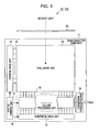
- Fig. 1 is a schematic illustration of an exemplary system configuration of a solid-state imaging device (e.g., a CMOS image sensor, which is an example of an X-Y addressing solid-state imaging device) according to a first exemplary embodiment of the present invention.
- a solid-state imaging device e.g., a CMOS image sensor, which is an example of an X-Y addressing solid-state imaging device
- a CMOS image sensor 10 includes a semiconductor substrate (hereinafter also referred to as a "sensor chip") 11.
- the sensor chip 11 includes a pixel array unit 12 formed thereon and a peripheral circuit unit integrated thereon.
- the peripheral circuit unit includes a vertical drive unit 13, a column processing unit 14, a horizontal drive unit 15, a conversion processing unit 16, and a system control unit 17.
- the pixel array unit 12 includes a plurality of unit pixels (not shown), each including a photoelectric conversion element, two-dimensionally arranged in an array.
- the unit pixel (hereinafter also simply referred to as a "pixel") photoelectrically converts visible light incident thereon into electrical charge in accordance with the intensity of the visible light.
- a color filter array 30 is provided on the pixel array unit 12 on the side of a light receiving surface (a light incident surface).
- One of the key features of the present exemplary embodiment is the color coding of the color filter array 30. The color coding of the color filter array 30 is described in more detail below.
- a pixel drive line 18 is disposed in the left-right direction of Fig. 1 (a direction in which the pixels of a pixel row are arranged or the horizontal direction) for each of the rows of the pixel array.
- a vertical signal line 19 is disposed in the up-down direction of Fig. 1 (a direction in which the pixels of a pixel column are arranged or the vertical direction) for each of the columns of the pixel array.
- the number of the pixel drive lines 18 is not limited to one.
- One end of the pixel drive line 18 is connected to an output terminal corresponding to one of the rows of the vertical drive unit 13.
- the vertical drive unit 13 includes a shift register and an address decoder. Although the detailed configuration thereof is not shown in Fig. 1 , the vertical drive unit 13 includes a readout scanning system and a sweeping scanning system. The readout scanning system sequentially scans the unit pixels from which signals are read by a row-by-row basis.
- the sweeping scanning system performs sweeping scanning so that unnecessary electrical charge is swept (reset) out of the photoelectric conversion elements of the unit pixels in the readout row.
- sweeping (resetting) the unnecessary electrical charge using the sweeping scanning system a so-called electronic shutter operation is performed. That is, in the electronic shutter operation, the photocharges of the photoelectric conversion element is discarded, and a new exposure operation (accumulation of light electrical charge) is started.
- a signal read through a readout operation performed by the readout scanning system corresponds to the amount of light made incident after the immediately previous readout operation or electronic shutter operation is performed.
- a period of time from a readout time point of the immediately previous readout operation or a sweeping time point of the electronic shutter operation to the readout time point of the current readout operation corresponds to an accumulation time (an exposure time) of the light electrical charge in the unit pixel.
- a signal output from each of the unit pixels in the pixel row selected and scanned by the vertical drive unit 13 is supplied to the column processing unit 14 via the corresponding one of the vertical signal lines 19.
- the column processing unit 14 performs predetermined signal processing on the analog pixel signal output from the pixel in the selected row.
- An example of the signal processing performed by the column processing unit 14 is a correlated double sampling (CDS) process.
- CDS correlated double sampling
- the reset level and the signal level output from each of the pixels in the selected row are retrieved, and the difference between the levels is computed.
- the signals of the pixels in one of the rows are obtained.
- fixed pattern noise of the pixels is removed.
- the column processing unit 14 may have an analog-to-digital (A/D) conversion function for converting the analog pixel signal into a digital format.
- the horizontal drive unit 15 includes a shift register and an address decoder.
- the horizontal drive unit 15 sequentially selects and scans a circuit portion corresponding to a pixel column of the column processing unit 14.
- Each of the pixel columns is sequentially processed by the column processing unit 14 through the selection scanning operation performed by the horizontal drive unit 15 and is sequentially output.
- the conversion processing unit 16 performs computation and converts signals corresponding to the color arrangement of the color filter array (the color filter unit) 30 and output from the pixels of the pixel array unit 12 into signals corresponding to the Bayer arrangement. Another of the key features of the present embodiment is that the conversion processing unit 16 is mounted on the substrate on which the pixel array unit 12 is formed, that is, the sensor chip 11, a color conversion process is performed in the sensor chip 11, and a signal corresponding to the Bayer arrangement is output from the sensor chip 11. The color conversion process performed by the conversion processing unit 16 is described in more detail below.
- the term "Bayer arrangement” represents a color arrangement in which a color serving as a primary color information component of a luminance signal for high resolution is arranged in a checkerboard pattern, and the other two colors serving as color information components of the luminance signal for not-so-high resolution are arranged in the other area of the checkerboard pattern.
- green (G) that has high contribution of the luminance signal is arranged in a checkerboard pattern
- red (R) and blue (B) are arranged in the other area of the checkerboard pattern.
- the system control unit 17 receives a clock provided from outside the sensor chip 11 and data for indicating an operating mode. In addition, the system control unit 17 outputs data representing internal information of the CMOS image sensor 10. Furthermore, the system control unit 17 includes a timing generator that generates a variety of timing signals. The system control unit 17 controls driving of the vertical drive unit 13, the column processing unit 14, the horizontal drive unit 15, and the conversion processing unit 16 using the variety of timing signals generated by the timing generator.
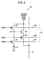
- Fig. 2 is an exemplary circuit diagram of a unit pixel 20.
- the unit pixel 20 illustrated in the exemplary circuit diagram includes a photoelectric conversion element (e.g., a photodiode 21) and four transistors (e.g., a transfer transistor 22, a reset transistor 23, an amplifying transistor 24, and a selection transistor 25).
- a photoelectric conversion element e.g., a photodiode 21
- transistors e.g., a transfer transistor 22, a reset transistor 23, an amplifying transistor 24, and a selection transistor 25.
- N-channel MOS transistors are used for the transfer transistor 22, the reset transistor 23, the amplifying transistor 24, and the selection transistor 25.
- the combination of a conductive type using the transfer transistor 22, the reset transistor 23, the amplifying transistor 24, and the selection transistor 25 is only an example, and the combination is not limited thereto.
- a transfer line 181, a reset line 182, and a selection line 183 are provided to each of the unit pixels 20 in the same pixel row.
- One end of the transfer line 181, one end of the reset line 182, and one end of the selection line 183 are connected to an output terminal corresponding to one of the pixel rows of the vertical drive unit 13.
- An anode electrode of the photodiode 21 is connected to a negative power supply (e.g., the ground).
- the photodiode 21 photoelectrically converts received light into photocharges (photoelectrons in this exemplary embodiment) in accordance with the amount of received light.
- a cathode electrode of the photodiode 21 is connected to the gate electrode of the amplifying transistor 24 via the transfer transistor 22.
- a node 26 electrically connected to the gate electrode of the amplifying transistor 24 is referred to as a "floating diffusion (FD) unit".
- the transfer transistor 22 is connected between the cathode electrode of the photodiode 21 and the FD unit 26.
- a transfer pulse ⁇ TRF having an active high level e.g., a Vdd level
- the transfer transistor 22 is turned on.
- the transfer transistor 22 transfers the photocharges photoelectrically converted by the photodiode 21 to the FD unit 26.
- a drain electrode of the reset transistor 23 is connected to a pixel power supply Vdd.
- the source electrode of the reset transistor 23 is connected to the FD unit 26.
- a high active reset pulse ⁇ RST is supplied to a gate electrode of the reset transistor 23 via the reset line 182.
- the reset transistor 23 is turned on.
- the reset transistor 23 resets the FD unit 26 by discarding the electrical charge of the FD unit 26 to the pixel power supply Vdd.
- the gate electrode of the amplifying transistor 24 is connected to the FD unit 26.
- a drain electrode of the amplifying transistor 24 is connected to the pixel power supply Vdd.
- the amplifying transistor 24 outputs the potential of the FD unit 26 in the form of a reset signal (a reset level) Vreset.
- the amplifying transistor 24 outputs the potential of the FD unit 26 in the form of a light accumulation signal (a signal level) Vsig.
- a drain electrode of the selection transistor 25 is connected to the source electrode of the amplifying transistor 24.
- the source electrode of the selection transistor 25 is connected to the vertical signal line 17.
- a high active selection pulse ⁇ SEL is supplied to the gate electrode of the selection transistor 25 via the selection line 163, the selection transistor 25 is turned on.
- the selection transistor 25 causes the unit pixel 20 to enter a selected mode so that a signal output from the amplifying transistor 24 is relayed to the vertical signal line 17.
- the pixel structure of the unit pixel 20 is not limited to the above-described four-transistor pixel structure.
- the unit pixel 20 may have a three-transistor pixel structure in which the functions of the amplifying transistor 24 and the selection transistor 25 are performed by one transistor.
- any configuration of a pixel circuit can be employed.
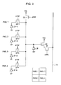
- Fig. 3 is a circuit diagram of an exemplary configuration of a circuit that allows pixel addition for four neighboring pixels to be performed in the pixels. The same numbering will be used in describing Fig. 3 as was utilized above in describing Fig. 2 , where appropriate.
- the photodiodes 21 of the four pixels arranged so as to be adjacent to one another in the vertical direction and the horizontal direction are denoted as photodiodes 21-1, 21-2, 21-3, and 21-4.
- Four transfer transistors 22-1, 22-2, 22-3, and 22-4 are provided to the photodiodes 21-1, 21-2, 21-3, and 21-4, respectively.
- the one reset transistor 23, the one amplifier transistor 24, and the one selection transistor 25 are used.
- one of the electrodes of the transfer transistor 22-1, one of the electrodes of the transfer transistor 22-2, one of the electrodes of the transfer transistor 22-3, and one of the electrodes of the transfer transistor 22-4 are connected to the cathode electrode of the photodiode 21-1, the cathode electrode of the photodiode 21-2, the cathode electrode of the photodiode 21-2, and the cathode electrode of the photodiode 21-2, respectively.
- the other electrode of the transfer transistor 22-1, the other electrode of the transfer transistor 22-2, the other electrode of the transfer transistor 22-3, and the other electrode of the transfer transistor 22-4 are commonly connected to the gate electrode of the amplifier transistor 24.
- the FD unit 26 that is shared by the photodiodes 21-1, 21-2, 21-3, and 21-4 is electrically connected to the gate electrode of the amplifier transistor 24.
- the drain electrode of the reset transistor 23 is connected to the pixel power supply Vdd, and the source electrode of the reset transistor 23 is connected to the FD unit 26.
- pixel addition for four neighboring pixels can be performed. That is, the signal charges transferred from the photodiodes 21-1, 21-2, 21-3, and 21-4 to the FD unit 26 by the four transfer transistors 22-1, 22-2, 22-3, and 22-4 are summed by the FD unit 26.
- signal output can be performed on a pixel-by-pixel basis. That is, when a moving image is captured, the frame rate can be increased by performing pixel addition. In contrast, when a still image is captured, the resolution can be increased by independently reading the signals of all of the pixels.
- the color filter array 30 employs color coding in which a color serving as a primary color information component of a luminance signal is arranged in a checkerboard pattern, and a plurality of the other colors are arranged in the other area of the checkerboard pattern.
- the primary color of a luminance signal is, for example, one of white (W), green (G), and another spectral component of the luminance signal.
- a W filter Since a W filter has a sensitivity about twice that of a G filter (the output level of a W filter is higher than that of a G filter), a high S/N ratio can be obtained. However, since a W filter contains various color information, a false color which is different from the original color of a subject tends to appear. In contrast, although a G filter has sensitivity lower than that of a W filter, a G filter produces few false colors. That is, there is a trade-off between the sensitivity and generation of a false color.
- R, G, and B filters are arranged in the other areas of the checkerboard pattern as filters of the other color information components.
- R and B filters are arranged in the other areas of the checkerboard pattern as filters of the other color information components.
- the sensitivity of the CMOS image sensor 10 can be increased, since the W filter has a sensitivity higher than that of a filter of another color.
- color coding in which G filters for the primary color of a luminance signal are arranged in a checkerboard pattern the color reproducibility of the CMOS image sensor 10 can be increased, since the G filter produces few false colors.
- a signal corresponding to the color arrangement is converted into a signal corresponding to the Bayer arrangement by the sensor chip 11.
- the color serving as the primary component of a luminance signal is arranged in a checkerboard pattern, signals of other colors of pixels adjacent to the color in the vertical direction and the horizontal direction can be restored using the signal of the color serving as the primary component of a luminance signal. Consequently, the efficiency of color conversion performed by the conversion processing unit 16 can be increased.
- an existing DSP for the Bayer arrangement can be used as a downstream signal processing unit.
- the DSP for the Bayer arrangement generates a luminance signal Y and two color difference signals U(B - Y) and V(R - Y) using the signal output from the sensor chip 11 and corresponding to the Bayer arrangement.
- Fig. 4 is a color arrangement diagram illustrating color coding according to a first example of the first exemplary embodiment.
- W filters that maximize the output level are arranged in a checkerboard pattern.
- R filters are arranged in a checkerboard pattern at a two-pixel pitch in the vertical direction and the horizontal direction.
- B filters are arranged in a checkerboard pattern at a two-pixel pitch in the vertical direction and the horizontal direction.
- Each of the R filters is diagonally shifted from one of the B filters by one pixel.
- G filters are arranged in the other area of the checkerboard pattern.
- W filters are arranged in a checkerboard pattern.
- R filters are arranged in the second row and first column and in the fourth row and third column.
- B filters are arranged in the first row and second column and in the third row and fourth column.
- This array is the checkerboard pattern having a two-pixel pitch.
- G filters are arranged in the other area of the checkerboard pattern. At that time, the G filters form a diagonal stripe pattern.
- Fig. 5 is a color arrangement diagram illustrating color coding according to a second example of the first exemplary embodiment.
- W filters are arranged in a checkerboard pattern.
- R filters are squarely arranged in the pattern at a four-pixel pitch in the vertical direction and the horizontal direction.
- B filters are squarely arranged in the pattern at a four-pixel pitch in the vertical direction and the horizontal direction.
- each of the R filters is diagonally shifted from one of the B filters by one pixel.
- G filters are arranged in the other area in the checkerboard pattern.
- W filters are arranged in a checkerboard pattern.
- An R filter is disposed in the second row and third column.
- a B filter is disposed in the third row and second column.
- This array is the square array having a four-pixel pitch in the vertical direction and the horizontal direction.
- G filters are arranged in the other area of the checkerboard pattern. At that time, the G filters form a diagonal stripe pattern.
- Fig. 6 is a color arrangement diagram illustrating color coding according to a third example of the first exemplary embodiment.
- W filters are arranged in a checkerboard pattern.
- R filters are squarely arranged in a checkerboard pattern at a four-pixel pitch in the vertical direction and the horizontal direction.
- B filters are squarely arranged in a checkerboard pattern at a four-pixel pitch in the vertical direction and the horizontal direction.
- each of the R filters is diagonally shifted from one of the B filters by two pixels.
- G filters are arranged in the other area in the checkerboard pattern.
- W filters are arranged in a checkerboard pattern.
- An R filter is disposed in the second row and first column.
- a B filter is disposed in the fourth row and third column.
- This array is the square array having a four-pixel pitch in the vertical direction and the horizontal direction.
- G filters are arranged in the other area of the checkerboard pattern. At that time, the G filters form a diagonal stripe pattern.
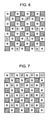
- Fig. 7 is a color arrangement diagram illustrating color coding according to a fourth example of the first exemplary embodiment.
- W filters are arranged in a checkerboard pattern.
- Filters of each of R and B are arranged in a checkerboard pattern at a two-pixel pitch in the vertical direction and the horizontal direction.
- each of the R filters is diagonally shifted from one of the B filters by one pixel.
- G filters are arranged in the other area in the checkerboard pattern.
- W filters are arranged in a checkerboard pattern.
- R filters are disposed in the first row and second column and in the third row and fourth column.
- B filters are disposed in the third row and second column and in the first row and fourth column.
- This array is the checkerboard array having a two-pixel pitch in the vertical direction and the horizontal direction.
- G filters are arranged in the other area of the checkerboard pattern.
- Fig. 8 is a color arrangement diagram illustrating color coding according to a fifth example of the first exemplary embodiment.
- W filters are arranged in a checkerboard pattern.
- R filters are squarely arranged in a checkerboard pattern at a two-pixel pitch in the vertical direction and the horizontal direction.
- B filters are squarely arranged in a checkerboard pattern at a two-pixel pitch in the vertical direction and the horizontal direction.
- each of the R filters is diagonally shifted from one of the B filters by one pixel.
- W filters are arranged in a checkerboard pattern.
- R filters are disposed in the second row and first column, the second row and third column, the fourth row and first column, and the fourth row and third column.
- B filters are disposed in the first row and second column, the first row and fourth column, the third row and second column, and the third row and fourth column.
- This array is the square array having a two-pixel pitch in the vertical direction and the horizontal direction.
- Fig. 9 is a color arrangement diagram illustrating color coding according to a sixth example of the first exemplary embodiment.
- W filters are arranged in a checkerboard pattern.
- R filters are squarely arranged in a checkerboard pattern at a four-pixel pitch in the vertical direction and the horizontal direction.
- B filters are squarely arranged in a checkerboard pattern at a four-pixel pitch in the vertical direction and the horizontal direction.
- each of the R filters is diagonally shifted from one of the B filters by two pixels.
- G filters are arranged in the other area of the checkerboard pattern.
- W filters are arranged in a checkerboard pattern.
- R filters are disposed in the third row and fourth column and in the fourth row and third column.
- B filters are disposed in the first row and second column and in the second row and first column.
- This array is the square array having a four-pixel pitch in the vertical direction and the horizontal direction.
- G filters are arranged in the other area of the checkerboard pattern. At that time, the G filters form a diagonal stripe pattern.
- the color coding methods according to the above-described first to sixth examples of the first exemplary embodiment use a color arrangement in which W filters having a color serving as a primary component of a luminance signal that maximizes the output level are arranged in a checkerboard pattern. Since the filters of a white color (W) that includes R, G, and B color components are arranged in a checkerboard pattern, the accuracy of conversion into signals corresponding to the RGB Bayer arrangement can be increased.
- W white color
- the W filters are arranged in a checkerboard pattern, and a series of four G filters arranged in a diagonal direction repeatedly appears so that a diagonal stripe pattern is formed.
- the intensity of the luminance signal can be increased. Accordingly, the sensitivity (the S/N ratio) can be increased.
- each of the R filters is diagonally shifted from one of the B filters by one pixel. Accordingly, the efficiency of conversion into a signal corresponding to the Bayer arrangement can be increased.
- R filters are arranged so as to form a square array having a four-pixel pitch in the vertical direction and the horizontal direction
- B filters are arranged so as to form a square array having a four-pixel pitch in the vertical direction and the horizontal direction.
- the each of the R filters is diagonally shifted from one of the B filters by two pixels. Accordingly, the efficiency of conversion can be increased.
- the number of G filters can be large. Thus, the efficiency of conversion into the G color can be increased.
- a series of four G filters arranged in a diagonal direction repeatedly appears so that a diagonal stripe pattern is formed. Accordingly, in such color coding methods, by adding the signal of a G pixel or the signals of two G pixels adjacent to a W pixel to the signal of the W pixel and using the sum signal as a primary component of a luminance signal, a high sensitivity (a high S/N rate) can be provided without a decrease in resolution.
- This advantage can be provided not only when a series of four G filters arranged in a diagonal direction repeatedly appears so that a diagonal stripe pattern is formed, but also when a series of four G filters arranged in the vertical direction or the horizontal direction repeatedly appears so that a stripe pattern is formed.
- Fig. 10 is a color arrangement diagram illustrating color coding according to a seventh example of the first exemplary embodiment.
- G filters serving as color filters of a primary component of a luminance signal are arranged in a checkerboard pattern.
- R filters and B filters are arranged in a checkerboard pattern at a two-pixel pitch in the vertical direction and the horizontal direction.
- Each of the R filters is diagonally shifted from one of the B filters by two pixels.
- W filters are arranged in the other area of the checkerboard pattern.
- G filters are arranged in a checkerboard pattern.
- R filters are arranged in the first row and first column and in the third row and third column.
- B filters are arranged in the first row and third column and in the third row and first column.
- This array is the checkerboard pattern having a two-pixel pitch in each of the vertical direction and the horizontal direction.
- W filters are arranged in the other area of the checkerboard pattern.
- W or G filters serving as color filters of a primary component of a luminance signal are arranged in a checkerboard pattern.
- color coding is not limited to the color coding in which W or G filters are arranged in a checkerboard pattern. Color coding in which W or G filters are not arranged in a checkerboard pattern is described below with reference to eighth and ninth examples of the first exemplary embodiment.
- Fig. 11 is a color arrangement diagram illustrating color coding according to an eighth example of the first exemplary embodiment.
- each of 2 ⁇ 2 pixel blocks includes W, R, G, and B filters, and a pattern having a two-pixel pitch in the vertical direction and the horizontal direction is formed. More specifically, each of the W filters is disposed in an even row and an even column, each of the R filters is disposed in an even row and an odd column, each of the G filters is disposed in an odd row and an odd column, and each of the B filters is disposed in an odd row and an even column.
- Fig. 12 is a color arrangement diagram illustrating color coding according to a ninth example of the first exemplary embodiment.
- each of 2 ⁇ 2 pixel blocks includes R, G, or B filters, and these pixel blocks form the Bayer arrangement. More specifically, G filters are disposed in first and second rows and first and second columns and in third and fourth rows and third and fourth rows, B filters are disposed in the first and second rows and the third and fourth columns, and R filters are disposed in third and fourth rows and the first and second columns.
- a sensitivity ratio W:G:R:B is described next.
- a W filter pixel that has a high output signal level is saturated earlier than a pixel of other color filters. Accordingly, it is necessary that a sensitivity balance among W, G, R, and B pixels be sustained, that is, the sensitivity ratio W:G:R:B be adjusted by decreasing the sensitivity of the W filter pixel and increasing the sensitivities of the other color filter pixel relative to the sensitivity of the W filter pixel.
- the sensitivity ratio In order to adjusting the sensitivity ratio, widely used exposure control techniques can be used. More specifically, by adjusting the size of an on-chip microlens provided outside the color filter array 30 for each of the pixels of the color filter array 30, the balance among the amounts of light made incident on individual color pixels is sustainable (refer to, for example, Japanese Unexamined Patent Application Publication No. 9-116127 ). By using this technique and decreasing the size of an on-chip microlens for a W color to a size smaller than that for each of the other colors, the sensitivity of the W filter pixel can be decreased. In this way, the sensitivity of one of the other color filter pixel can be relatively increased.
- an exposure light control technique in which, in color coding including a W filter, the difference between the sensitivities can be reduced by removing an on-chip microlens for a W pixel, and a color S/N can be improved by increasing the color sensitivity can be used (refer to, for example, Japanese Unexamined Patent Application Publication No. 2007-287891 ).
- the sensitivity of the W filter pixel can be decreased. In this way, the sensitivity of one of the other color filter pixel can be relatively increased.
- a technique of performing shutter exposure control in which the exposure time of a G filter pixel is decreased compared with that for an R or B filter pixel can be used (refer to, for example, Japanese Unexamined Patent Application Publication No. 2003-60992 ).
- the sensitivity of the W filter pixel can be decreased.
- the sensitivity of one of the other color filter pixel can be relatively increased.
- the occurrence of a colored outline of a moving subject can be eliminated.
- an achromatizing process performed by an external signal processing unit (a DSP) is not necessary.
- the size of the on-chip microlens for a W pixel is set in such a manner that the output levels of the W, G, B, and R pixels are substantially in the proportion 2:1:0.5:0.5.
- the output level of a W pixel having an area the same as that of a G pixel and having an output level double that of the G pixel can be adjusted so that the output levels are the same.
- the area is ⁇ 1.42 times the original area and, therefore, the sensitivity of the W pixel can be reduced to 1.42 times that of the G pixel. In such a case, the further adjustment of the sensitivity may be performed by shutter exposure control.
- a process for converting a signal into a signal corresponding to the RGB Bayer arrangement i.e., a color conversion process
- the conversion processing unit 16 A process for converting a signal into a signal corresponding to the RGB Bayer arrangement (i.e., a color conversion process) performed by the conversion processing unit 16 is described in more detail next.
- the following two types of color conversion process are provided: a color conversion process performed when a still image is captured (at a time of full scanning in which all of the pixels are scanned) and a color conversion process performed when a moving image is captured (at a time of pixel addition in which signals of a plurality of pixels neighboring a given pixel is added to the signal of the given pixel).
- a color conversion process with a high sensitivity can be performed. Accordingly, a low luminance mode can be used and, therefore, the color conversion process performed at a time of full scanning can be divided into two color conversion processes.
- One of the two color conversion processes is performed when the luminance of incident light is higher than a predetermined reference luminance.
- This color conversion process is referred to as a "color conversion process 1".
- the other color conversion process is performed when the luminance of incident light is lower than or equal to the predetermined reference luminance.
- This color conversion process is referred to as a "color conversion process 2".
- the color conversion process performed at a time of pixel addition can be divided into a plurality of color conversion processes in accordance with the combinations of the pixels to be added.
- a color conversion process performed for the color coding according to the first example of the first exemplary embodiment is described next.
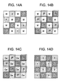
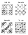
- the color conversion process 1 performed in a high luminance mode at a time of full scanning is described with reference to a flowchart shown in Fig. 13 and schematic illustrations shown in Figs. 14A to 14D .
- Fig. 14A illustrates a 4 ⁇ 4 pixel color arrangement of the color coding according to the first example.
- step S11 as shown in Fig. 14B , the components of white (W) pixels arranged in a checkerboard pattern are expanded into pixels of all colors by determining the direction of resolution.
- direction of resolution refers to a direction in which pixel signals are present.
- W surrounded by a square frame represents a component of a W pixel after the component of the W pixel is expanded into each of all colors.
- signal processing based on a widely used directional correlation can be applied.
- signal processing based on a directional correlation a plurality of color signals corresponding to a given pixel is acquired, and the correlation value in the vertical direction and/or the horizontal direction is obtained (refer to, for example, Japanese Patent No. 2931520 ).
- a W pixel is replaced with a G pixel using a correlation between a W pixel and a G pixel.
- a W pixel is adjacent to a G pixel.
- the W pixel and the G pixel have a strong correlation since either one of the W pixel and the G pixel has a color serving as a primary component of a luminance signal.
- the correlation value is nearly 1.
- step S13 an R pixel and a B pixel are generated for the Bayer arrangement shown in Fig. 14D using a correlation between the W pixel and the R pixel and a correlation between the W pixel and the B pixel. Since a W pixel includes R, G, and B color components, the correlation between the W pixel and the R pixel and the correlation between the W pixel and the B pixel can be obtained.
- an existing technique in which a luminance signal to be replaced with G in a four-color arrangement is generated for every pixel by interpolation can be used (refer to, for example, Japanese Unexamined Patent Application Publication No. 2005-160044 ).
- the direction of resolution is examined by using signal processing based on the above-described widely used technique (step S21). Thereafter, it is determined whether the direction of resolution can be determined (step S22). If the direction of resolution can be determined, the components of the W pixels arranged in a checkerboard pattern are expanded into pixels of all colors (step S23).
- R pixels and B pixels are generated using the above-described widely used technique, the correlation between a W pixel and an R pixel, and the correlation between a W pixel and a B pixel (step S24).
- each of the G pixels is generated for the Bayer arrangement (step S25).
- each of the R and B pixels is generated for the Bayer arrangement by using simple four-pixel averaging interpolation using four pixels adjacent to the W pixel in the vertical direction and the horizontal direction (step S26).
- signals corresponding to a color arrangement in which W filters are arranged in a checkerboard pattern can be converted into signals corresponding to the RGB Bayer arrangement on the sensor chip 11, and the signals can be output.
- pixel addition process 1 Two color conversion processes performed at a time of pixel addition for moving image capturing are described next.
- pixel addition process 1 one of the two color conversion processes is referred to as a "pixel addition process 1”
- pixel addition process 2 the other color conversion process is referred to as a "pixel addition process 2”.
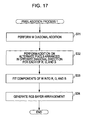
- pixel addition process 1 is described with reference to a flowchart shown in Fig. 17 and schematic illustrations shown in Figs. 18A to 18D .
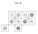
- Addition is performed on two W pixels diagonally adjacent to each other (step S31). More specifically, as shown in Fig. 18A , addition is performed on a pixel of interest and a pixel located to the lower right of the pixel of interest (i.e., a pixel to the right by one column and below by one row).
- This addition can be performed in the pixel structure shown in Fig. 3 by providing the transfer pulse ⁇ TRF to the transfer transistors 22 of the two pixels which are the targets of addition (the transfer transistors 22-1 and 22-4 in this example) at the same time. In this way, two-pixel addition can be performed in the FD unit 26.
- FD addition such pixel addition is referred to as "FD addition”.
- addition is performed on two pixels arranged with one pixel therebetween in the opposite diagonal direction (step S32). More specifically, as shown in Fig. 18B , addition is performed on a pixel of interest and a pixel located to the lower left of the pixel of interest with one pixel therebetween (i.e., a pixel to the right by two columns and below by two rows). For each of R, G, and B pixels, when the column processing unit 14 shown in Fig. 1 has an A/D conversion function, this addition can be performed during A/D conversion.
- the signals of pixels B1 and G1 are read independently. After the signals are A/D-converted, the signals of pixels B2 and G3 are continuously read and A/D-converted. In this way, two-pixel addition can be performed.
- an existing technique for converting an analog pixel signal into a digital pixel signal using a counter can be used (refer to, for example, Japanese Unexamined Patent Application Publication No. 2006-033454 ).
- counter addition this pixel addition performed using a counter of an A/D converter is referred to as "counter addition”.
- counter addition is performed and if the gain is changed on a line-by-line basis, the addition ratio can be varied.
- counter addition can be performed on R pixels. Note that, in the above-described two-pixel addition for the W pixels, FD addition is performed between the pixels W1 and W2 and between the pixels W3 and W4.
- step S34 the components of the W pixel are fitted into the R, G, and B pixels.
- step S34 the components of the W pixel are fitted into the R, G, and B pixels.
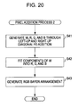
- pixel addition process 2 is described with reference to a flowchart shown in Fig. 20 and schematic illustrations shown in Figs. 21A to 21D .
- FD addition is performed between two pixels arranged in the upper left-bottom right diagonal directions and the upper right-bottom left diagonal directions, respectively.
- W, R, G, and B pixels are generated (step S41). More specifically, for the W pixels, as shown in Fig. 21A , FD addition is performed between a pixel of interest and a pixel located at the lower right of the pixel of interest (i.e., a pixel to the right by one column and below by one row).
- FD addition is performed between a pixel of interest and a pixel located at the lower left of the pixel of interest (i.e., a pixel to the left by one column and below by one row).
- Fig. 21C the components of the W pixel are fitted into the R, G, and B pixels (step S42).
- step S42 the components of the W pixel are fitted into the R, G, and B pixels.
- step S43 four pixels for the RGB Bayer arrangement are generated (step S43).
- the centroid location of the Bayer arrangement is slightly shifted from that in the pixel addition process 1.
- step S51 For each of W, R, G, and B pixels, addition is performed between two pixels arranged in a diagonal direction with a pixel therebetween (step S51).
- a color arrangement including a row of R, W, G, W, ... and the next row of W, G, W, R, ... is obtained after the addition.
- Fig. 23C in a manner the same as that in the process at a time of full scanning, R and B pixels are generated for the Bayer arrangement using the correlation between a W pixel and an R pixel and the correlation between a W pixel and an R pixel (step S52).
- signals corresponding to a color arrangement in which W filters are arranged in a checkerboard pattern can be converted into signals corresponding to the RGB Bayer arrangement on the sensor chip 11, and the signals can be output.
- Color conversion processes for color coding according to the second to ninth examples are described below. In many cases, the process sequence is similar to that of the first example.
- FIG. 24A A color conversion process at a time of full scanning is described with reference to schematic illustrations shown in Figs. 24A to 24D .
- the components of W pixels arranged in a checkerboard pattern are expanded into pixels of all colors using the direction of resolution, as shown in Fig. 24B .
- the W pixels are replaced with G pixels using a correlation between a W pixel and a G pixel.
- R and B pixels are generated for the RGB Bayer arrangement using a correlation between a W pixel and an R pixel and a correlation between a W pixel and a B pixel.
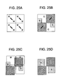
- Figs. 25A to 25D The pixel addition process is described next with reference to schematic illustrations shown in Figs. 25A to 25D .
- Figs. 25A and 25B for a W pixel and a G pixel, FD addition is performed between two pixels located in the bottom right-upper left diagonal directions and bottom left-upper right diagonal directions, respectively.
- W, R, G, and B pixels are generated.
- Fig. 25C the components of the W pixels are fitted into the R, G, and B pixels.
- Fig. 25D four pixels for the RGB Bayer arrangement are generated.
- FIG. 26A A color conversion process at a time of full scanning is described with reference to schematic illustrations shown in Figs. 26A to 26D .
- the components of W pixels arranged in a checkerboard pattern are expanded into pixels of all colors using the direction of resolution, as shown in Fig. 26B .
- the W pixels are replaced with G pixels using a correlation between a W pixel and a G pixel.
- R and B pixels are generated for the RGB Bayer arrangement using a correlation between a W pixel and an R pixel and a correlation between a W pixel and a B pixel.
- Figs. 27A to 27E The pixel addition process is described next with reference to schematic illustrations shown in Figs. 27A to 27E .
- Figs. 27A and 27B for W, R, G, and B pixels, left-up and right-up diagonal FD addition is performed.
- W, Cy (cyan), G, and Ye (yellow) colors are generated.
- the components of the W pixels are fitted into the R, G, and B pixels.
- Fig. 27E four pixels for the RGB Bayer arrangement are generated.
- FIG. 28A A color conversion process at a time of full scanning is described first with reference to schematic illustrations shown in Figs. 28A to 28D .
- the components of W pixels arranged in a checkerboard pattern are expanded into pixels of all colors using the direction of resolution, as shown in Fig. 28B .
- the W pixels are replaced with G pixels using a correlation between a W pixel and a G pixel.
- R and B pixels are generated for the RGB Bayer arrangement using a correlation between a W pixel and an R pixel and a correlation between a W pixel and a B pixel.
- the four types of pixel addition can be used.
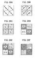
- the first type of pixel addition is described next with reference to schematic illustrations shown in Figs. 29A to 29F .
- Figs. 29A and 29B for R and B pixels, addition is performed on alternate pixels arranged in the upper left-bottom right diagonal directions and the upper right-bottom left diagonal directions.
- W, Cy, and Ye colors are generated.
- Fig. 29C each of the Cy and Ye components is expanded into all pixels.
- the components of the W pixels are then fitted into the R, G, and B pixels.
- Fig. 29F four pixels for the RGB Bayer arrangement are generated.
- Figs. 30A to 30D The second type of pixel addition is described next with reference to schematic illustrations shown in Figs. 30A to 30D .
- Fig. 30A for R pixels and B pixels, addition is performed between two alternate pixels arranged in the upper left-bottom right diagonal directions and in the upper right-bottom left diagonal directions, respectively.
- G pixels an average value of the G value located at the center and four G pixels located immediately above and beneath the center pixel and to the left and right of the center pixel is computed.
- W pixels as shown in Fig. 30B , diagonal FD addition is performed.
- Fig. 30C the components of the W pixels are then fitted into the R, G, and B pixels.
- Fig. 30D four pixels for the RGB Bayer arrangement are generated.
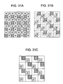
- Figs. 31A to 31C The third type of pixel addition is described next with reference to schematic illustrations shown in Figs. 31A to 31C .
- Fig. 31A for W pixels, addition is performed between two diagonally adjacent pixels.
- the components of the W pixels are then fitted into the R, G, and B pixels.
- Fig. 31C four pixels for the RGB Bayer arrangement are generated.
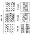
- Figs. 32A to 32D The fourth type of pixel addition is described next with reference to schematic illustrations shown in Figs. 32A to 32D .
- Fig. 32A for each of W, R, G, and B pixels, diagonal two-pixel FD addition with one pixel therebetween is performed. Thereafter, by combining the signals of the W pixels arranged in a two-row-based checkerboard pattern, a color arrangement including a W checkerboard pattern can be obtained, as shown in Fig. 32B .
- the W pixels are replaced with G pixels using a correlation between a W pixel and a G pixel, as shown in Fig. 32C .
- Fig. 32D R and B pixels are generated for the RGB Bayer arrangement using a correlation between a W pixel and an R pixel and a correlation between a W pixel and a B pixel.
- FIG. 33A A color conversion process at a time of full scanning is described first with reference to schematic illustrations shown in Figs. 33A to 33D .
- the components of W pixels arranged in a checkerboard pattern are expanded into pixels of all colors using the direction of resolution, as shown in Fig. 33B .
- the components of each of R and B pixels are expanded into all pixels using a correlation between a W pixel and an R pixel and a correlation between a W pixel and a B pixel.
- G W - R - B is computed.
- the components of the W pixels are fitted into all pixels.
- Fig. 33D four pixels for the RGB Bayer arrangement are generated.
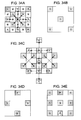
- Figs. 34A to 34E The pixel addition is described next with reference to schematic illustrations shown in Figs. 34A to 34E .
- Fig. 34A the centroid locations of R, G, and B pixels are aligned.
- the signals of R pixels are summed.
- the signals of G pixels are summed, and the signals of B pixels are summed.
- Fig. 34C diagonal direction four-pixel addition is performed for the B pixels, and up-and-down left-and-right five-pixel addition is performed for the R pixels.
- the R pixels and the B pixels are generated.
- Fig. 34D four pixels for the RGB Bayer arrangement are generated.
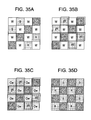
- a color conversion process 1 at a time of full scanning is described first with reference to schematic illustrations shown in Figs. 35A to 35D .
- the components of W pixels arranged in a checkerboard pattern are expanded into pixels of all colors using the direction of resolution, as shown in Fig. 35B .
- the W pixels are replaced with G pixels using a correlation between a W pixel and a G pixel.
- R and B pixels are generated for the RGB Bayer arrangement using a correlation between a W pixel and an R pixel and a correlation between a W pixel and a B pixel.
- a color conversion process 2 at a time of full scanning is described next with reference to schematic illustrations shown in Figs. 36A to 36D .
- the components of W pixels arranged in a checkerboard pattern are expanded into pixels of all colors using the direction of resolution, as shown in Fig. 36A .
- R and B pixels are generated using a correlation between a W pixel and an R pixel and a correlation between a W pixel and a B pixel.
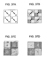
- the pixel addition process 1 is described next with reference to Figs. 37A to 37D .
- Figs. 37A and 37B left-up and right-up diagonal FD addition is performed for a W pixel and each of R, G, and B pixels.
- W, R, G, and B pixels are generated.
- Fig. 37C the components of the W pixel are fitted into each of the pixels.
- Fig. 37D four pixels for the RGB Bayer arrangement are generated.
- a pixel addition process 2 is described next with reference to Figs. 38A to 38D .
- Figs. 38A and 38B left-up and right-up diagonal FD addition is performed for a W pixel and each of R, G, and B pixels.
- W, R, G, and B pixels are generated.
- Fig. 38C the components of the W pixel are fitted into each of the R and B pixels.
- Fig. 38D four pixels for the RGB Bayer arrangement are generated.
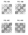
- FIG. 39A A color conversion process at a time of full scanning is described first with reference to schematic illustrations shown in Figs. 39A to 39D .
- the components of G pixels arranged in a checkerboard pattern are expanded into R and B pixels using the direction of resolution, as shown in Fig. 39B .
- the W pixels are replaced with the R and B pixels using a correlation between a W pixel and an R pixel and a correlation between a W pixel and a B pixel.
- Fig. 39D four pixels for the RGB Bayer arrangement are generated.
- FIG. 40A A pixel addition process is described next with reference to schematic illustrations shown in Figs. 40A to 40E .
- Fig. 40A for R pixels and B pixels, addition is performed between two alternate pixels arranged in the upper left-bottom right diagonal directions and in the upper right-bottom left diagonal directions, respectively.
- Fig. 40B 2R and 2B pixels are generated.
- Fig. 40C diagonal diamond-shape addition is performed on G pixels.
- Fig. 40D 4G pixels are generated.
- Gw, Rw, and Bw are added to the W pixels using a correlation between a W pixel and an R pixel, a correlation between a W pixel and a B pixel, and a correlation between a W pixel and a B pixel.
- a correlation between a W pixel and an R pixel a correlation between a W pixel and a B pixel
- a correlation between a W pixel and a B pixel a correlation between a W pixel and a B pixel.
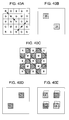
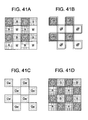
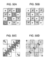
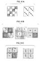
- FIG. 41A A color conversion process at a time of full scanning is described with reference to schematic illustrations shown in Figs. 41A to 41D .
- the component of W pixels are expanded into the G and W pixels so as to be arranged in a checkerboard pattern using the direction of resolution, as shown in Fig. 41B .
- the components of the W pixels are fitted into the G pixels.
- Fig. 41D four pixels for the RGB Bayer arrangement are generated.
- Figs. 42A to 42D The pixel addition process is described next with reference to schematic illustrations shown in Figs. 42A to 42D .
- Fig. 42A the centroid locations of G and W pixels are aligned.
- the signals of G pixels are summed, and the signals of W pixels are summed.
- Fig. 42B the components of the W pixels are fitted into the G pixels.
- G G + Gw is generated.
- Fig. 42C diagonal direction four-pixel addition is performed for the B pixels, and up-and-down left-and-right five-pixel addition is performed for the R pixels.
- Fig. 42D four pixels for the RGB Bayer arrangement are generated.
- FIG. 43A A color conversion process at a time of full scanning is described with reference to schematic illustrations shown in Figs. 43A to 43C .
- the components of the G pixels are expanded into R and B pixels using the direction of resolution, as shown in Fig. 43B .
- Fig. 43C four pixels for the RGB Bayer arrangement are generated using a correlation between a G pixel and an R pixel and a correlation between a G pixel and a B pixel.
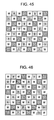
- FD addition is performed on the signals of four pixels of a 2 ⁇ 2 pixel block of the same color.
- Fig. 44B four pixels for the RGB Bayer arrangement are generated.
- Fig. 1 is a schematic illustration of an exemplary system configuration of a CMOS image sensor, which is an example of a solid-state imaging device (an X-Y addressing solid-state imaging device) according to a second exemplary embodiment based on the first exemplary embodiment.
- each of CMOS image sensors 10, 10A, 10B, ... includes a semiconductor substrate (hereinafter also referred to as a "sensor chip") 11, a pixel array unit 12, a vertical drive unit 13, a column processing unit 14, a horizontal drive unit 15, a conversion processing unit 16, a system control unit 17, and a color filter array (a color filter unit) 30.
- a unit pixel 20 includes a photodiode 21, a transfer transistor 22, a reset transistor 23, an amplifying transistor 24, and a selection transistor 25, and a floating diffusion (FD) unit 26.
- a reference numeral "40" denotes a DSP circuit.
- the pixel array unit 12 is formed on the semiconductor substrate (the sensor chip) 11.
- a peripheral circuit unit is integrated onto the semiconductor substrate 11 having the pixel array unit 12 formed thereon.
- the peripheral circuit unit includes the vertical drive unit 13, the column processing unit 14, the horizontal drive unit 15, the conversion processing unit 16, and the system control unit 17.
- the pixel array unit 12 includes a plurality of unit pixels (not shown), each including a photoelectric conversion element, two-dimensionally arranged in an array.
- the unit pixel (hereinafter also simply referred to as a "pixel") photoelectrically converts visible light incident thereon into electrical charge in accordance with the intensity of the visible light.
- the color filter array 30 is provided on the pixel array unit 12 on the side of a light receiving surface (a light incident surface).
- One of the key features of the present exemplary embodiment is the color coding of the color filter array 30. The color coding of the color filter array 30 is described in more detail below.
- a pixel drive line 18 is disposed in the left-right direction of Fig. 1 (a direction in which the pixels of a pixel row are arranged or the horizontal direction) for each of the rows of the pixel array.
- a vertical signal line 19 is disposed in the up-down direction of Fig. 1 (a direction in which the pixels of a pixel column are arranged or the vertical direction) for each of the columns of the pixel array.
- the number of the pixel drive lines 18 is not limited to 1.
- One end of the pixel drive line 18 is connected to an output terminal corresponding to one of the rows of the vertical drive unit 13.
- the vertical drive unit 13 includes a shift register and an address decoder. Although the detailed configuration thereof is not shown in Fig. 1 , the vertical drive unit 13 includes a readout scanning system and a sweeping scanning system. The readout scanning system sequentially scans the unit pixels from which signals are read by a row-by-row basis.
- the sweeping scanning system performs sweeping scanning so that unnecessary electrical charge is swept (reset) out of the photoelectric conversion elements of the unit pixels in the readout row.
- sweeping (resetting) the unnecessary electrical charge using the sweeping scanning system a so-called electronic shutter operation is performed. That is, in the electronic shutter operation, the light electrical charge of the photoelectric conversion element is discarded, and a new exposure operation (accumulation of light electrical charge) is started.
- a signal read through a readout operation performed by the readout scanning system corresponds to the amount of light made incident after the immediately previous readout operation or electronic shutter operation is performed.
- a period of time from a readout time point of the immediately previous readout operation or a sweeping time point of the electronic shutter operation to the readout time point of the current readout operation corresponds to an accumulation time (an exposure time) of the light electrical charge in the unit pixel.
- a signal output from each of the unit pixels in the pixel row selected and scanned by the vertical drive unit 13 is supplied to the column processing unit 14 via the corresponding one of the vertical signal lines 19.
- the column processing unit 14 performs predetermined signal processing on the analog pixel signal output from the pixel in the selected row.
- An example of the signal processing performed by the column processing unit 14 is a correlated double sampling (CDS) process.
- CDS correlated double sampling
- the reset level and the signal level output from each of the pixels in the selected row are retrieved, and the difference between the levels is computed.
- a signal of the pixels in the selected row is obtained.
- fixed pattern noise of the pixels is removed.
- the column processing unit 14 may have an analog-to-digital (A/D) conversion function for converting the analog pixel signal into a digital format.
- the horizontal drive unit 15 includes a shift register and an address decoder.
- the horizontal drive unit 15 sequentially selects and scans a circuit portion corresponding to a pixel column of the column processing unit 14.
- Each of the pixel columns is sequentially processed by the column processing unit 14 through the selection scanning operation performed by the horizontal drive unit 15 and is sequentially output.
- the conversion processing unit 16 performs computation and converts signals corresponding to the color arrangement of the color filter array (the color filter unit) 30 and output from the pixels of the pixel array unit 12 via the column processing unit 14 into signals corresponding to the Bayer arrangement. Another of the key features of the present embodiment is that the conversion processing unit 16 is mounted on the substrate on which the pixel array unit 12 is formed, that is, the sensor chip 11, a color conversion process is performed in the sensor chip 11, and a signal corresponding to the Bayer arrangement is output from the sensor chip 11. The color conversion process performed by the conversion processing unit 16 is described in more detail below.
- the term "Bayer arrangement” represents a color arrangement in which a color serving as a primary color information component of a luminance signal for high resolution is arranged in a checkerboard pattern, and the other two colors serving as color information components of the luminance signal for not-so-high resolution are arranged in the other area of the checkerboard pattern.
- green (G) that has high contribution of the luminance signal is arranged in a checkerboard pattern
- red (R) and blue (B) are arranged in the other area of the checkerboard pattern.
- the system control unit 17 receives a clock provided from outside the sensor chip 11 and data for indicating an operating mode. In addition, the system control unit 17 outputs data representing internal information of the CMOS image sensor 10. Furthermore, the system control unit 17 includes a timing generator that generates a variety of timing signals. The system control unit 17 controls driving of the vertical drive unit 13, the column processing unit 14, the horizontal drive unit 15, and the conversion processing unit 16 using the variety of timing signals generated by the timing generator.
- Fig. 2 is an exemplary circuit diagram of a unit pixel 20.
- the unit pixel 20 illustrated in the exemplary circuit diagram includes a photoelectric conversion element (e.g., a photodiode 21) and four transistors (e.g., a transfer transistor 22, a reset transistor 23, an amplifying transistor 24, and a selection transistor 25).
- a photoelectric conversion element e.g., a photodiode 21
- transistors e.g., a transfer transistor 22, a reset transistor 23, an amplifying transistor 24, and a selection transistor 25.
- N-channel MOS transistors are used for the transfer transistor 22, the reset transistor 23, the amplifying transistor 24, and the selection transistor 25.
- the combination of a conductive type using the transfer transistor 22, the reset transistor 23, the amplifying transistor 24, and the selection transistor 25 is only an example, and the combination is not limited thereto.
- a transfer line 181, a reset line 182, and a selection line 183 are provided to each of the unit pixels 20 in the same pixel row.
- One end of the transfer line 181, one end of the reset line 182, and one end of the selection line 183 are connected to an output terminal corresponding to one of the pixel rows of the vertical drive unit 13.
- An anode electrode of the photodiode 21 is connected to a negative power supply (e.g., the ground).
- the photodiode 21 photoelectrically converts received light into photocharges (photoelectrons in this exemplary embodiment) in accordance with the amount of received light.
- a cathode electrode of the photodiode 21 is connected to the gate electrode of the amplifying transistor 24 via the transfer transistor 22.
- a node 26 electrically connected to the gate electrode of the amplifying transistor 24 is referred to as a "floating diffusion (FD) unit".
- the transfer transistor 22 is connected between the cathode electrode of the photodiode 21 and the FD unit 26.
- a transfer pulse ⁇ TRF having an active high level e.g., a Vdd level
- the transfer transistor 22 is turned on.
- the transfer transistor 22 transfers the photocharges photoelectrically converted by the photodiode 21 to the FD unit 26.
- a drain electrode of the reset transistor 23 is connected to a pixel power supply Vdd.
- the source electrode of the reset transistor 23 is connected to the FD unit 26.
- a high active reset pulse ⁇ RST is supplied to a gate electrode of the reset transistor 23 via the reset line 182.
- the reset transistor 23 is turned on.
- the reset transistor 23 resets the FD unit 26 by discharging the electrical charge of the FD unit 26 to the pixel power supply Vdd.
- the gate electrode of the amplifying transistor 24 is connected to the FD unit 26.
- a drain electrode of the amplifying transistor 24 is connected to the pixel power supply Vdd.
- the amplifying transistor 24 outputs the potential of the FD unit 26 in the form of a reset signal (a reset level) Vreset.
- the amplifying transistor 24 outputs the potential of the FD unit 26 in the form of a light accumulation signal (a signal level) Vsig.
- a drain electrode of the selection transistor 25 is connected to the source electrode of the amplifying transistor 24.
- the source electrode of the selection transistor 25 is connected to the vertical signal line 17.
- a high active selection pulse ⁇ SEL is supplied to the gate electrode of the selection transistor 25 via the selection line 163, the selection transistor 25 is turned on.
- the selection transistor 25 causes the unit pixel 20 to enter a selected mode so that a signal output from the amplifying transistor 24 is relayed to the vertical signal line 17.
- the pixel structure of the unit pixel 20 is not limited to the above-described four-transistor pixel structure.
- the unit pixel 20 may have a three-transistor pixel structure in which the functions of the amplifying transistor 24 and the selection transistor 25 are performed by one transistor.
- any configuration of a pixel circuit can be employed.
- pixel addition in which signals output from a plurality of neighboring pixels are summed and read out is performed.
- the pixel addition is performed in a pixel, signal lines, the column processing unit 14, or a downstream signal processing unit.
- a pixel structure in which four pixels arranged so as to be adjacent to one another in the vertical direction and the horizontal direction is described.
- Fig. 3 is a circuit diagram of an exemplary configuration of a circuit that allows pixel addition for four neighboring pixels to be performed in the pixels. The same numbering will be used in describing Fig. 3 as was utilized above in describing Fig. 2 , where appropriate.
- the photodiodes 21 of the four pixels arranged so as to be adjacent to one another in the vertical direction and the horizontal direction are denoted as photodiodes 21-1, 21-2, 21-3, and 21-4.
- Four transfer transistors 22-1, 22-2, 22-3, and 22-4 are provided to the photodiodes 21-1, 21-2, 21-3, and 21-4, respectively.
- the one reset transistor 23, the one amplifier transistor 24, and the one selection transistor 25 are used.
- one of the electrodes of the transfer transistor 22-1, one of the electrodes of the transfer transistor 22-2, one of the electrodes of the transfer transistor 22-3, and one of the electrodes of the transfer transistor 22-4 are connected to the cathode electrode of the photodiode 21-1, the cathode electrode of the photodiode 21-2, the cathode electrode of the photodiode 21-3, and the cathode electrode of the photodiode 21-4, respectively.
- the other electrode of the transfer transistor 22-1, the other electrode of the transfer transistor 22-2, the other electrode of the transfer transistor 22-3, and the other electrode of the transfer transistor 22-4 are commonly connected to the gate electrode of the amplifier transistor 24.
- the FD unit 26 that is shared by the photodiodes 21-1, 21-2, 21-3, and 21-4 is electrically connected to the gate electrode of the amplifier transistor 24.
- the drain electrode of the reset transistor 23 is connected to the pixel power supply Vdd, and the source electrode of the reset transistor 23 is connected to the FD unit 26.
- pixel addition for four neighboring pixels can be performed. That is, the signal charges transferred from the photodiodes 21-1, 21-2, 21-3, and 21-4 to the FD unit 26 by the four transfer transistors 22-1, 22-2, 22-3, and 22-4 are summed by the FD unit 26.
- the signals can be output on a pixel-by-pixel basis. That is, when a moving image is captured, the frame rate can be increased by performing pixel addition. In contrast, when a still image is captured, the resolution can be increased by independently reading the signals of all of the pixels.
- the color filter array 30 employs color coding in which filters of a first color serving as one of primary color information components of a luminance signal are arranged in a checkerboard pattern.
- filters of a second color of the primary color information components for a series of four pixels form a group, and the groups are arranged so as to form a stripe pattern in one of a diagonal direction, a vertical direction, and a horizontal direction.
- the filters of a first color and a second color of the primary colors of a luminance signal are, for example, a W filter and a G filter.
- the filters of W and G colors which are primary components of a luminance signal have sensitivities higher than those of filters of other colors (more specifically, R and B filters).
- the W filter has sensitivity about twice that of the G filter. Accordingly, by arranging the W and G filters (in particular, the W filters) in a checkerboard pattern, the sensitivity (the S/N ratio) can be increased.
- the sensitivity the S/N ratio
- a W filter contains various color information, a false color which is different from the original color of a subject tends to appear.
- a G filter has sensitivity lower than that of a W filter, a G filter produces few false colors. That is, there is a trade-off between the sensitivity and generation of a false color.
- R, G, and B filters are arranged in the other areas of the checkerboard pattern for the other color information components.
- R and B filters are arranged in the other areas of the checkerboard pattern for the other color information components.
- CMOS image sensor 10A when the color filter array 30 using either one of the color coding methods is used, a signal corresponding to the color arrangement is converted into a signal corresponding to the Bayer arrangement by the sensor chip 11. At that time, since the color serving as the primary component of a luminance signal is arranged in a checkerboard pattern, signals of other colors of pixels adjacent to the color in the vertical direction and the horizontal direction can be restored using the signal of the color serving as the primary component of a luminance signal. Consequently, the efficiency of color conversion performed by the conversion processing unit 16 can be increased.
- an existing DSP for the Bayer arrangement can be used as a downstream signal processing unit.
- the DSP for the Bayer arrangement generates a luminance signal Y and two color difference signals U(B - Y) and V(R - Y) using the signal output from the sensor chip 11 and corresponding to the Bayer arrangement.
- Fig. 45 is a color arrangement diagram illustrating color coding according to a first example of the second exemplary embodiment.
- W filters are arranged in a checkerboard pattern.
- R filters are arranged in a checkerboard pattern at a two-pixel pitch in the vertical direction and the horizontal direction.
- B filters are arranged in a checkerboard pattern at a two-pixel pitch in the vertical direction and the horizontal direction.
- one of the R filters is diagonally shifted from one of the B filters by one pixel.
- G filters are arranged in the other area of the checkerboard pattern.
- W filters are arranged in a checkerboard pattern.
- R filters are arranged in the second row and first column and in the fourth row and third column.
- B filters are arranged in the first row and second column and in the third row and fourth column.
- This array is the checkerboard pattern having a two-pixel pitch.
- G filters are arranged in the other area of the checkerboard pattern. At that time, the G filters form a diagonal stripe pattern.
- Fig. 46 is a color arrangement diagram illustrating color coding according to a second example of the second exemplary embodiment.
- W filters are arranged in a checkerboard pattern.
- R filters are squarely arranged in a checkerboard pattern at a four-pixel pitch in the vertical direction and the horizontal direction.
- B filters are squarely arranged in a checkerboard pattern at a four-pixel pitch in the vertical direction and the horizontal direction.
- the R filters and the B filters are diagonally shifted from each other by two pixels.
- G filters are arranged in the other area in the checkerboard pattern.
- W filters are arranged in a checkerboard pattern.
- R filters are disposed in the third row and fourth column.
- B filters are disposed in the first row and second column and in the second row and first column.
- This array is the square array having a four-pixel pitch in the vertical direction and the horizontal direction.
- G filters are arranged in the other area of the checkerboard pattern. At that time, the G filters form a diagonal stripe pattern.
- the color coding methods according to the above-described first and second examples use a color arrangement in which W filters having a color serving as a primary component of a luminance signal that maximizes the output level are arranged in a checkerboard pattern. Since the W filters that include R, G, and B color components are arranged in a checkerboard pattern, the conversion accuracy of a signal corresponding to the RGB Bayer arrangement can be increased.
- the key feature of the color coding methods according to the first and second examples of the second exemplary embodiment is that the W filters are arranged in a checkerboard pattern, and a series of four G filters arranged in a diagonal direction repeatedly appears so that a diagonal stripe pattern is formed.
- the intensity of the luminance signal can be increased. Accordingly, the sensitivity (the S/N ratio) can be increased.
- the R filters are arranged in a checkerboard pattern at a two-pixel pitch in the vertical direction and in the horizontal direction.
- each of the R filters is diagonally shifted from one of the B filters by one pixel. Accordingly, the efficiency of conversion into a signal corresponding to the Bayer arrangement can be increased.
- a series of four G filters arranged in a diagonal direction repeatedly appears so that a diagonal stripe pattern is formed. Accordingly, in such color coding methods, by adding the signal of a G pixel or the signals of G pixels adjacent to a W pixel to the signal of the W pixel and using the sum signal as a primary component of a luminance signal, a high sensitivity (a high S/N ratio) can be provided without a decrease in resolution.
- This advantage can be provided not only when a series of four G filters arranged in a diagonal direction repeatedly appears so that a diagonal stripe pattern is formed, but also when a series of four G filters arranged in the vertical direction or the horizontal direction repeatedly appears so that a stripe pattern is formed.
- a sensitivity ratio W:G:R:B is described next.
- a W filter pixel that has a high output signal level is saturated earlier than a pixel of other color filters. Accordingly, it is necessary that a sensitivity balance among W, G, R, and B pixels be sustained, that is, the sensitivity ratio W:G:R:B be adjusted by decreasing the sensitivity of the W filter pixel and increasing the sensitivities of the other color filter pixel relative to the sensitivity of the W filter pixel.
- the sensitivity ratio In order to adjusting the sensitivity ratio, widely used exposure control techniques can be used. More specifically, by adjusting the size of an on-chip microlens provided outside the color filter array 30 for each of the pixels of the color filter array 30, the balance among the amounts of light made incident on individual colors is sustainable (refer to, for example, Japanese Unexamined Patent Application Publication No. 9-116127 ). By using this technique and decreasing the size of an on-chip microlens for a W color than that for one of the other colors, the sensitivity of the W filter pixel can be decreased. In this way, the sensitivity of one of the other color filter pixel can be relatively increased.
- an exposure light control technique in which, in color coding including a W filter, the difference between the sensitivities can be reduced by removing an on-chip microlens for a W pixel, and a color S/N can be improved by increasing the color sensitivity can be used (refer to, for example, Japanese Unexamined Patent Application Publication No. 2007-287891 ).
- the sensitivity of the W filter pixel can be decreased. In this way, the sensitivity of one of the other color filter pixel can be relatively increased.
- a technique for preventing the improper color balance by performing shutter exposure control in which the exposure time of a G filter pixel is decreased compared with that for an R or B filter pixel can be used (refer to, for example, Japanese Unexamined Patent Application Publication No. 2003-60992 ).
- the sensitivity of the W filter pixel can be decreased.
- the sensitivity of one of the other color filter pixel can be relatively increased.
- the occurrence of a colored outline of a moving subject can be eliminated.
- an achromatizing process performed by an external signal processing unit (a DSP) is not necessary.
- the size of the on-chip microlens for a W pixel is set in such a manner that the output levels of the W, G, B, and R pixels are substantially in the proportion 2:1:0.5:0.5.
- the output level of a W pixel having an area the same as that of a G pixel and having an output level double that of the G pixel can be adjusted so that the output levels are the same.
- the area is ⁇ 1.42 times the original area and, therefore, the sensitivity of the W pixel can be reduced to 1.42 times that of the G pixel. In such a case, the further adjustment of the sensitivity may be performed by shutter exposure control.
- a process for converting the signals into signals corresponding to the RGB Bayer arrangement i.e., a color conversion process
- a color conversion process performed by the conversion processing unit 16 is described in more detail next.
- the following two types of color conversion process are provided: a color conversion process performed when a still image is captured (at a time of full scanning in which all of the pixels are scanned) and a color conversion process performed when a moving image is captured (at a time of pixel addition in which signals of a plurality of pixels neighboring a pixel is added to the signal of the pixel).
- a color conversion process with a high sensitivity can be performed. Accordingly, a low luminance mode can be used and, therefore, the color conversion process performed at a time of full scanning can be divided into two color conversion processes.
- One of the two color conversion processes is performed when the luminance of incident light is higher than a predetermined reference luminance.
- This color conversion process is referred to as a "color conversion process 1".
- the other color conversion process is performed when the luminance of incident light is lower than or equal to the predetermined reference luminance.
- This color conversion process is referred to as a "color conversion process 2".
- the color conversion process performed at a time of pixel addition can be divided into a plurality of color conversion processes in accordance with the combinations of the pixels to be added.
- a color conversion process performed for the color coding according to the first example of the second exemplary embodiment is described next.
- the color conversion process 1 performed in a high luminance mode at a time of full scanning is described with reference to a flowchart shown in Fig. 13 and schematic illustrations shown in Figs. 14A to 14D .
- Fig. 14A illustrates a 4 ⁇ 4 color arrangement of the color coding according to the first example.
- step S11 as shown in Fig. 14B , the components of white (W) pixels arranged in a checkerboard pattern are expanded into pixels of all colors by determining the direction of resolution.
- direction of resolution refers to a direction in which pixel signals are present.
- W surrounded by a transparent square represents a component of a W pixel after the component of the W pixel is expanded into each of all colors.
- signal processing based on a widely used directional correlation can be applied.
- signal processing based on a directional correlation a plurality of color signals corresponding to a given pixel is acquired, and the correlation value in the vertical direction and/or the horizontal direction is obtained (refer to, for example, Japanese Patent No. 2931520 ).
- a W pixel is replaced with a G pixel using a correlation between a W pixel and a G pixel.
- a W pixel is adjacent to a G pixel.
- the W pixel and the G pixel have a strong correlation since either one of the W pixel and the G pixel has a color serving as a primary component of a luminance signal.
- the correlation value is nearly 1.
- step S13 an R pixel and a B pixel are generated for the Bayer arrangement shown in Fig. 14D using correlation between the W pixel and the R pixel and correlation between the W pixel and the B pixel. Since a W pixel includes R, G, and B color components, the correlation between the W pixel and the R pixel and the correlation between the W pixel and the B pixel can be obtained.
- an existing technique in which a luminance signal to be replaced with G in a four-color arrangement is generated for every pixel by interpolation can be used (refer to, for example, Japanese Unexamined Patent Application Publication No. 2005-160044 ).
- the direction of resolution is examined by using signal processing based on the above-described directional correlation (step S21). Thereafter, it is determined whether the direction of resolution can be determined (step S22). If the direction of resolution can be determined, the components of the W pixels arranged in a checkerboard pattern are expanded into pixels of all colors (step S23).
- R pixels and B pixels are generated using the correlation between a W pixel and an R pixel and the correlation between a W pixel and a B pixel (step S24).
- each of the R and B pixels is generated for the Bayer arrangement (step S25).
- each of the R and B pixels is generated for the Bayer arrangement by using simple four-pixel averaging interpolation using four pixels adjacent to the W pixel in the vertical direction and the horizontal direction (step S26).
- signals corresponding to a color arrangement in which W filters are arranged in a checkerboard pattern can be converted into signals corresponding to the RGB Bayer arrangement on the sensor chip 11, and the signals can be output.
- pixel addition process 1 Two color conversion processes performed at a time of pixel addition for moving image capturing are described next.
- pixel addition process 1 one of the two color conversion processes is referred to as a "pixel addition process 1”
- pixel addition process 2 the other color conversion process is referred to as a "pixel addition process 2”.
- Addition is performed on two W pixels diagonally adjacent to each other (step S31). More specifically, as shown in Fig. 48A , addition is performed on a pixel of interest and a pixel located to the lower right of the pixel of interest (i.e., a pixel to the right by one column and below by one row).
- This addition can be performed in the pixel structure shown in Fig. 3 by providing the transfer pulse ⁇ TRF to the transfer transistors 22 of the two pixels which are the targets of addition (the transfer transistors 22-1 and 22-4 in this example) at the same time. In this way, two-pixel addition can be performed in the FD unit 26.
- FD addition such pixel addition is referred to as "FD addition”.
- addition is performed on two pixels arranged in the opposite diagonal direction and having one pixel therebetween (step S32). More specifically, as shown in Fig. 48B , addition is performed on a pixel of interest and a pixel located to the lower left of the pixel of interest with one pixel there between (i.e., a pixel to the right by two columns and below by two rows). For each of R, G, and B pixels, when the column processing unit 14 shown in Fig. 1 has an A/D conversion function, this addition can be performed during A/D conversion.
- the signals of pixels B1 and G1 are read independently. After the signals are A/D-converted, the signals of pixels B2 and G3 are continuously read and A/D-converted. In this way, two-pixel addition can be performed.
- an existing technique for converting an analog pixel signal into a digital pixel signal using a counter can be used (refer to, for example, Japanese Unexamined Patent Application Publication No. 2006-033454 ).
- counter addition this pixel addition performed using a counter of an A/D converter is referred to as "counter addition”.
- counter addition is performed and if the gain is changed on a line-by-line basis, the addition ratio can be varied.
- counter addition can be performed on R pixels. Note that, in the above-described two-pixel addition for the W pixels, FD addition is performed between the pixels W1 and W2 and between the pixels W3 and W4.
- step S34 the components of the W pixel are fitted into the R, G, and B pixels.
- step S34 the components of the W pixel are fitted into the R, G, and B pixels.
- pixel addition process 2 is described with reference to a flowchart shown in Fig. 20 and schematic illustrations shown in Figs. 21A to 21D .
- FD addition is performed between two pixels arranged in the upper left-bottom right diagonal directions and the upper right-bottom left diagonal directions, respectively.
- W, R, G, and B pixels are generated (step S41). More specifically, for the W pixels, as shown in Fig. 21A , FD addition is performed between a pixel of interest and a pixel located at the lower right of the pixel of interest (i.e., a pixel to the right by one column and below by one row).
- FD addition is performed between a pixel of interest and a pixel located at the lower left of the pixel of interest (i.e., a pixel to the left by one column and below by one row).
- Fig. 21C the components of the W pixel are fitted into the R, G, and B pixels (step S42).
- step S42 the components of the W pixel are fitted into the R, G, and B pixels.
- step S43 four pixels for the RGB Bayer arrangement are generated (step S43).
- the centroid location of the Bayer arrangement is slightly shifted from that in the pixel addition process 1.
- signals corresponding to a color arrangement in which W filters are arranged in a checkerboard pattern can be converted into signals corresponding to the RGB Bayer arrangement on the sensor chip 11, and the signals can be output.
- a color conversion process for the color coding according to the second example of the second exemplary embodiment is described next.
- a series of processes for the color coding according to the second example of the second exemplary embodiment is based on that for the color coding according to the first example of the second exemplary embodiment.
- a color conversion process 1 at a time of full scanning is described with reference to schematic illustrations shown in Figs. 49A to 49D .
- the components of W pixels arranged in a checkerboard pattern are expanded into pixels of all colors using the direction of resolution, as shown in Fig. 49B .
- the W pixels are replaced with G pixels using a correlation between a W pixel and a G pixel.
- R and B pixels are generated for the RGB Bayer arrangement using a correlation between a W pixel and an R pixel and a correlation between a W pixel and a B pixel.
- a color conversion process 2 at a time of full scanning is described next with reference to schematic illustrations shown in Figs. 50A to 50D .
- the components of W pixels arranged in a checkerboard pattern are expanded into pixels of all colors using the direction of resolution, as shown in Fig. 50A .
- R pixels and B pixels are generated using a correlation between a W pixel and an R pixel and a correlation between a W pixel and a B pixel.
- Figs. 51A to 51D The pixel addition process 1 is described next with reference to Figs. 51A to 51D .
- Figs. 51A and 51B left-up and right-up diagonal FD addition is performed for a W pixel and each of R, G, and B pixels.
- W, R, G, and B pixels are generated.
- Fig. 51C the components of the W pixel are fitted into each of the pixels.
- Fig. 51D four pixels for the RGB Bayer arrangement are generated.
- a color conversion process 2 is described next with reference to Figs. 52A to 52D .
- Figs. 52A and 52B left-up and right-up diagonal FD addition is performed for a W pixel and each of R, G, and B pixels.
- W, R, G, and B pixels are generated.
- Fig. 51C the components of the W pixel are fitted into each of the R and B pixels.
- Fig. 52D four pixels for the RGB Bayer arrangement are generated.
- the following advantage can be provided. That is, by adding the signal of a G pixel adjacent to a W pixel to the signal of the W pixel and performing signal processing using the sum as a primary component of the luminance signal, the intensity of the luminance signal can be increased. Accordingly, the sensitivity can be increased with a minimal decrease in resolution.
- Fig. 53 is a schematic illustration of an exemplary system configuration of a CMOS image sensor, which is an example of a solid-state imaging device (an X-Y addressing solid-state imaging device) according to a third exemplary embodiment. The same numbering will be used in describing Fig. 53 as was utilized above in describing Fig. 1 , where appropriate.
- the conversion processing unit 16 disposed on the sensor chip 11 converts signals corresponding to the color arrangement of the color filter array 30 into signals corresponding to the RGB Bayer arrangement.
- W, R, G, and B signals corresponding to the color arrangement of the color filter array 30 are directly output from the sensor chip 11 in the form of raw data.
- the CMOS image sensor 10B allows a DSP circuit 40, which is an external circuit of the sensor chip 11, to perform a color conversion process on the raw data output from the sensor chip 11.
- the DSP circuit 40 converts the W, R, G, and B signals output from the sensor chip 11 into signals corresponding to the RGB Bayer arrangement. Thereafter, the DSP circuit 40 performs a widely used demosaic process. In the demosaic process, color information is added to the signal of each of the pixels that has only monochrome information by supplying missing color information using the signals of pixels surrounding the pixel, and a full-color image is generated.
- the key feature of the CMOS image sensor 10B according to the present embodiment is that the W, R, G, and B signals corresponding to the color arrangement of the color filter array 30 are directly output from the sensor chip 11 and are converted into the signals corresponding to the RGB Bayer arrangement by the DSP circuit 40. Accordingly, since the configurations and operations of the pixel array unit 12, the vertical drive unit 13, the column processing unit 14, the horizontal drive unit 15, and the system control unit 17 are similar to those of the second exemplary embodiment, the descriptions thereof are not repeated.
- the CMOS image sensor 10B has color coding of the color filter array 30 that facilitates conversion into signals corresponding to the RGB Bayer arrangement.
- the color filter array 30 employs color coding in which filters of a first color (W or G) serving as one of primary color information components of a luminance signal are arranged in a checkerboard pattern.
- filters of a second color (G or W) of the primary color information components for a series of four pixels form a group, and the groups are arranged so as to form a stripe pattern in one of a diagonal direction, a vertical direction, and a horizontal direction.
- first and second examples of color coding can be provided.
- the first and second examples facilitate conversion from a signal corresponding to a color arrangement in which filters of a color serving as a primary component of a luminance signal are arranged in a checkerboard pattern into a signal corresponding to an RGB Bayer arrangement.
- W filters are arranged in a checkerboard pattern.
- R filters are arranged in a checkerboard pattern at a two-pixel pitch in the vertical direction and the horizontal direction.
- B filters are arranged in a checkerboard pattern at a two-pixel pitch in the vertical direction and the horizontal direction.
- each of the R filters is diagonally shifted from one of the B filters by one pixel.
- G filters are arranged in the other area of the checkerboard pattern (refer to Fig. 45 ).
- W filters are arranged in a checkerboard pattern.
- R filters are squarely arranged at a four-pixel pitch in the vertical direction and the horizontal direction.
- B filters are squarely arranged at a four-pixel pitch in the vertical direction and the horizontal direction.
- two of the R filters and two of the B filters are alternately arranged in a diagonal direction.
- G filters are arranged in the other area in the checkerboard pattern (refer to Fig. 46 ).
- a process performed by the DSP circuit 40 for converting signals that correspond to the color arrangement of the color filter array 30 and that are output from the sensor chip 11 in the form of raw data into signals corresponding to the RGB Bayer arrangement is described in more detail next.
- the pixel sensitivity ratio of W:G:R:B is adjusted.
- the following two types of color conversion process are provided: a color conversion process performed at a time of full scanning and a color conversion process performed at a time of pixel addition.
- the following two types of color conversion process are provided: a color conversion process 1 performed in a high luminance mode in which the luminance of incident light is higher than a predetermined reference luminance and a color conversion process 2 performed in a low luminance mode in which the luminance of incident light is lower than or equal to the reference luminance.
- a color conversion process performed in the case of color coding according to the first example of the third exemplary embodiment is described next.
- the color conversion process 1 performed in a high luminance mode at a time of full scanning is described with reference to a flowchart shown in Fig. 54 and schematic illustrations shown in Figs. 55A to 55C .
- Fig. 55A illustrates a 4 ⁇ 4 pixel color arrangement of the color coding according to the first example of the third exemplary embodiment.
- the components of the W pixels are expanded into pixels of all colors by using the above-described existing signal process using directional correlation and determining the direction of resolution (step S51).
- Fig. 55C by using the above-described existing technique and a correlation between a W pixel and an R pixel, a correlation between a W pixel and a G pixel, and a correlation between a W pixel and a B pixel, the R, G, and B components are expanded into all pixels (step S52).
- the direction of resolution is examined by using signal processing based on the above-described directional correlation (step S61). Thereafter, it is determined whether the direction of resolution can be determined (step S62). If the direction of resolution can be determined, the components of the W pixels arranged in a checkerboard pattern are expanded into pixels of all colors (step S63).
- R pixels and B pixels are generated by using the above-described existing technique and the correlation between a W pixel and an R pixel and the correlation between a W pixel and a B pixel (step S64).
- each of the R and B pixels is generated by using simple four-pixel averaging interpolation using four pixels adjacent to the W pixel in the vertical direction and the horizontal direction (step S67).
- step S65 the signals of two G pixels adjacent to the W pixel are added to the signal of the W pixel (W + 2G) while dynamically changing the ratio.
- step S65 the components are expanded into all pixels by determining the direction. In this way, a luminance signal is generated (step S66).
- the signals corresponding to a color arrangement in which W filters are arranged in a checkerboard pattern can be converted into signals corresponding to the RGB Bayer arrangement through signal processing performed by the DSP circuit 40 disposed outside the sensor chip 11.
- the color conversion processes 1 and 2 performed at a time of pixel addition for capturing a moving image are described next.
- the pixel addition process 1 is described with reference to a flowchart shown in Fig. 58 and schematic illustrations shown in Figs. 59A to 59C .
- step S71 addition is performed on two W pixels diagonally adjacent to each other.
- counter addition is performed on two pixels arranged in a diagonal direction (step S71).
- step S71 R components, G components, and B components are expanded into all pixels using a correlation between a W pixel and an R pixel, a correlation between a W pixel and a G pixel, and a correlation between a W pixel and a B pixel (step S72).
- step S72 the signals of the W pixel and the G signal are added in proportion 1:2, and a (W + 2G) signal is generated.
- the (W + 2G) signals serve as luminance signals (step S73).
- the pixel addition process 2 is described next with reference to a flowchart shown in Fig. 60 and schematic illustrations shown in Figs. 61A to 61C .
- FD addition is performed between two pixels arranged in the upper left-bottom right diagonal directions and the upper right-bottom left diagonal direction, respectively.
- W and G pixels are generated (step S81). More specifically, for the G pixels, FD addition is performed between a pixel of interest and a pixel located at the lower left of the pixel of interest (i.e., a pixel to the left by one column and below by one row).
- FD addition is performed between a pixel of interest and a pixel located at the lower right of the pixel of interest (i.e., a pixel to the right by one column and below by one row).
- the R and B pixels remain unchanged.
- the R, G, and B components are expanded into all pixels using the correlation between a W pixel and an R pixel, the correlation between a W pixel and a G pixel, and the correlation between a W pixel and a B pixel (step S82).
- the signals of the W pixel and the G signal are added in proportion 1:2, and a (W + 2G) signal is generated.
- the (W + 2G) signals serve as luminance signals (step S83).
- the signals corresponding to a color arrangement in which W filters are arranged in a checkerboard pattern can be converted into signals corresponding to the RGB Bayer arrangement through signal processing performed by the DSP circuit 40 disposed outside the sensor chip 11.
- a color conversion process for the color coding according to the second example of the third exemplary embodiment is described next.
- a series of processes for the color coding according to the second example of the third exemplary embodiment is generally based on that for the color coding according to the first example of the third exemplary embodiment.
- Fig. 62A illustrates a color arrangement of color coding of a 4 ⁇ 4 pixel block according to the second example of the third exemplary embodiment.
- Fig. 62B illustrates the components of W pixels arranged in a checkerboard pattern into pixels of all colors using the direction of resolution. Subsequently, as shown in Fig.
- the R, G, and B components are expanded into all pixels using the correlation between a W pixel and an R pixel, the correlation between a W pixel and a G pixel, and the correlation between a W pixel and a B pixel.
- the color conversion process 2 performed at a time of full scanning is described next with reference to schematic illustrations shown in Figs. 63A to 63C .
- the components of W pixels arranged in a checkerboard pattern are expanded into pixels of all colors using the direction of resolution.
- the R and B components are expanded into all pixels using the correlation between a W pixel and an R pixel and the correlation between a W pixel and a B pixel.
- Fig. 63C by determining the direction using the W pixels, the signals of two G pixels adjacent to the W pixel are added to the signal of the W pixel while dynamically changing the ratio (W + 2G). Thus, a checkerboard pattern is formed.
- the components of the G pixels are expanded into all pixels by further determining the direction. In this way, a luminance signal is generated.
- the pixel addition process 1 is described next with reference to Figs. 64A and 64B .
- Fig. 64A for W pixels and G pixels, FD addition is performed between two pixels arranged in the upper left-bottom right diagonal directions and the upper right-bottom left diagonal directions, respectively.
- the signals of W, R, G, and B pixels are generated.
- Fig. 64B the R, G, and B components are expanded into all of the pixels.
- the components of the W pixels are fitted into all of the pixels.
- R, G, and B signals are generated.
- the pixel addition process 2 is described next with reference to Figs. 65A to 65C .
- Fig. 65A for W pixels and G pixels, FD addition is performed between two pixels arranged in the upper left-bottom right diagonal directions and the upper right-bottom left diagonal directions, respectively.
- the signals of W, R, G, and B pixels are generated.
- Fig. 65B the R, G, and B components are expanded into all pixels using the correlation between a W pixel and an R pixel, the correlation between a W pixel and a G pixel, and the correlation between a W pixel and a B pixel.
- the signals of the W pixel and the G signal are then added in proportion 1:2, and a (W + 2G) signal is generated.
- the (W + 2G) signals serve as luminance signals.
- the following advantage can be provided by performing the above-described signal processing. That is, in the DSP circuit 40 provided outside the sensor chip 11, by adding the signal of a G pixel adjacent to a W pixel to the signal of the W pixel and performing signal processing using the sum as a primary component of the luminance signal, the intensity of the luminance signal can be increased. Accordingly, the sensitivity can be increased with a minimal decrease in resolution.
- the number of the G pixels used for addition is not limited to two.
- the number of the G pixels may be one. Note that 2-pixel addition in which the signal of one G pixel adjacent to a W pixel is added to the signal of the W pixel has an advantage over 3-pixel addition in which the signals of two G pixels adjacent to a W pixel are added to the signal of the W pixel in that it can reduce a decrease in resolution.
- the addition ratio of the signal of a filter of a first color to that of a second color is not limited to 1:1. Any addition ratio that balances the resolution with the sensitivity can be used.
- Fig. 68 is a block diagram of an exemplary configuration of an imaging apparatus according to an embodiment of the present invention.
- an imaging apparatus 100 includes an optical system including a lens unit 101, an image pickup device 102, a DSP circuit 103 serving as a camera signal processing circuit, a frame memory 104, a display unit 105, a recording unit 106, an operation unit 107, and a power supply unit 108.
- the DSP circuit 103, the frame memory 104, the display unit 105, the recording unit 106, the operation unit 107, and the power supply unit 108 are connected to one another via a bus line 109.
- the lens unit 101 receives incident light (imaging light) output from a subject and forms an image on an imaging surface of the image pickup device 102.
- the image pickup device 102 converts the intensity of the incident light that is received by the lens unit 101 and that forms an image on the imaging surface into an electrical signal for each pixel.
- the electrical signals are output in the form of pixel signals.
- the CMOS image sensors 10A and 10B according to the first and second exemplary embodiments can be used as the image pickup device 102.
- the CMOS image sensor 10 according to all of the above-described exemplary embodiments (including the third exemplary embodiment) can be used as the image pickup device 102.
- the color filter array employs color coding having a color arrangement in which a color serving as a primary color of a luminance signal is arranged in a checkerboard pattern, and a plurality of colors serving as color information components are arranged in the other area of the checkerboard pattern.
- the CMOS image sensors 10A and 10 convert signals corresponding to the color arrangement of the color filter array into signals corresponding to the Bayer arrangement through computation performed in the sensor chip 11.
- the CMOS image sensors 10A and 10 have the color filter array using color coding in which a color serving as a primary color of a luminance signal is arranged in a checkerboard pattern, the CMOS image sensors 10A and 10 output signals corresponding to the Bayer arrangement. Consequently, an existing DSP for the Bayer arrangement that generates a luminance signal Y and two color difference signals U (B - Y) and V (R - Y) using signals corresponding to the Bayer arrangement can be used as the DSP circuit 103.
- an existing DSP for the Bayer arrangement can be used, the development of a new DSP that is significantly costly is not necessary even when the color coding of a color filter array used in the image pickup device 102 is changed.
- the use of an existing DSP can contribute to cost reduction in the production of the imaging apparatus 100 including the DSP circuit 103 and, in particular, to widespread use of a color filter array having color coding using a W filter.
- the CMOS image sensor 10B In contrast, in the case of the CMOS image sensor 10B, signals corresponding to a color arrangement in which a color serving as a primary color of a luminance signal is arranged in a checkerboard pattern are output to outside the chip, and the DSP circuit 103 (corresponding to the DSP circuit 40 shown in Fig. 52 ) converts the signals into signals corresponding to the Bayer arrangement. Accordingly, when the color coding of the color filter array is changed, the development of a new DSP circuit 103 is necessary and, therefore, the development cost is necessary. However, like the CMOS image sensor 10A, the CMOS image sensor 10B can increase the sensitivity with a minimal decrease in resolution. Accordingly, the CMOS image sensor 10B has an advantage in that it can increase the S/N ratio of an imaging signal while maintaining a high resolution.
- the display unit 105 is a panel display unit, such as a liquid crystal display or an organic electroluminescence (EL) display.
- the display unit 105 displays a moving image or a still image captured by the image pickup device 102.
- the recording unit 106 records a moving image or a still image captured by the image pickup device 102 on a recording medium, such as a video tape or a digital versatile disk (DVD).
- a recording medium such as a video tape or a digital versatile disk (DVD).
- the operation unit 107 submits a variety of operation commands that control a variety of functions of the imaging apparatus.
- the power supply unit 108 supplies electrical power to the DSP circuit 103, the frame memory 104, the display unit 105, the recording unit 106, and the operation unit 107 when necessary.
Landscapes
- Engineering & Computer Science (AREA)
- Physics & Mathematics (AREA)
- Multimedia (AREA)
- Signal Processing (AREA)
- General Physics & Mathematics (AREA)
- Optics & Photonics (AREA)
- Spectroscopy & Molecular Physics (AREA)
- Computer Vision & Pattern Recognition (AREA)
- Theoretical Computer Science (AREA)
- Color Television Image Signal Generators (AREA)
- Solid State Image Pick-Up Elements (AREA)
Applications Claiming Priority (2)
| Application Number | Priority Date | Filing Date | Title |
|---|---|---|---|
| JP2008311694A JP4683121B2 (ja) | 2008-12-08 | 2008-12-08 | 固体撮像装置、固体撮像装置の信号処理方法および撮像装置 |
| JP2008311695A JP4626706B2 (ja) | 2008-12-08 | 2008-12-08 | 固体撮像装置、固体撮像装置の信号処理方法および撮像装置 |
Publications (3)
| Publication Number | Publication Date |
|---|---|
| EP2194721A2 true EP2194721A2 (fr) | 2010-06-09 |
| EP2194721A8 EP2194721A8 (fr) | 2010-07-14 |
| EP2194721A3 EP2194721A3 (fr) | 2013-01-02 |
Family
ID=41559619
Family Applications (1)
| Application Number | Title | Priority Date | Filing Date |
|---|---|---|---|
| EP09015079A Withdrawn EP2194721A3 (fr) | 2008-12-08 | 2009-12-04 | Dispositif d'imagerie à l'état solide, procédé de traitement de signal pour dispositif d'imagerie à l'état solide et appareil d'imagerie |
Country Status (7)
| Country | Link |
|---|---|
| US (7) | US8436925B2 (fr) |
| EP (1) | EP2194721A3 (fr) |
| KR (1) | KR101624748B1 (fr) |
| CN (2) | CN101753863B (fr) |
| BR (1) | BRPI0904888A2 (fr) |
| RU (1) | RU2531368C2 (fr) |
| TW (1) | TWI422020B (fr) |
Cited By (8)
| Publication number | Priority date | Publication date | Assignee | Title |
|---|---|---|---|---|
| EP2822036A3 (fr) * | 2013-07-01 | 2015-04-29 | Omnivision Technologies, Inc. | Motifs de matrice de filtre couleur et infrarouge afin de réduire le repliement de couleur |
| US9667933B2 (en) | 2013-07-01 | 2017-05-30 | Omnivision Technologies, Inc. | Color and infrared filter array patterns to reduce color aliasing |
| WO2018077357A1 (fr) * | 2016-10-28 | 2018-05-03 | Conti Temic Microelectronic Gmbh | Capteur d'image pourvu de filtre de couleurs adapté au compartimentage de pixels |
| US10097782B2 (en) | 2014-10-31 | 2018-10-09 | Sony Semiconductor Solutions Corporation | Signal processing device and signal processing method |
| US10616509B2 (en) | 2015-02-12 | 2020-04-07 | Sony Corporation | Imaging device and control method thereof, and electronic apparatus |
| US11356624B2 (en) | 2016-11-15 | 2022-06-07 | Sony Semiconductor Solutions Corporation | Solid-state imaging element, signal processing circuit, and electronic equipment |
| US11571111B2 (en) | 2016-10-21 | 2023-02-07 | Olympus Corporation | Endoscope scope, endoscope processor, and endoscope adaptor |
| EP4214930A4 (fr) * | 2020-11-06 | 2023-07-26 | Guangdong Oppo Mobile Telecommunications Corp., Ltd. | Dispositif électrique, procédé de génération de données d'image et support non transitoire lisible par ordinateur |
Families Citing this family (104)
| Publication number | Priority date | Publication date | Assignee | Title |
|---|---|---|---|---|
| US7568628B2 (en) | 2005-03-11 | 2009-08-04 | Hand Held Products, Inc. | Bar code reading device with global electronic shutter control |
| US7611060B2 (en) | 2005-03-11 | 2009-11-03 | Hand Held Products, Inc. | System and method to automatically focus an image reader |
| US7780089B2 (en) | 2005-06-03 | 2010-08-24 | Hand Held Products, Inc. | Digital picture taking optical reader having hybrid monochrome and color image sensor array |
| US7770799B2 (en) | 2005-06-03 | 2010-08-10 | Hand Held Products, Inc. | Optical reader having reduced specular reflection read failures |
| JP5085140B2 (ja) * | 2007-01-05 | 2012-11-28 | 株式会社東芝 | 固体撮像装置 |
| JP4747154B2 (ja) * | 2007-11-22 | 2011-08-17 | 富士フイルム株式会社 | 固体撮像素子の駆動方法、固体撮像素子、及び撮像装置 |
| TWI422020B (zh) * | 2008-12-08 | 2014-01-01 | Sony Corp | 固態成像裝置 |
| JP5572960B2 (ja) | 2009-02-16 | 2014-08-20 | 株式会社ニコン | 撮像装置およびその画素加算方法 |
| JP5634194B2 (ja) * | 2010-09-28 | 2014-12-03 | キヤノン株式会社 | 放射線撮像装置及びその制御方法 |
| US8717255B2 (en) * | 2010-10-18 | 2014-05-06 | Vp Assets Limited | Image device with pixel dots with multi-primary colors |
| US8803767B2 (en) * | 2010-10-18 | 2014-08-12 | Vp Assets Limited | Image device with pixels arranged for white balance |
| US9093017B2 (en) | 2010-10-18 | 2015-07-28 | Vp Assets Limited | Image device with pixel dots with multi-primary colors |
| JP2012195921A (ja) * | 2011-02-28 | 2012-10-11 | Sony Corp | 固体撮像素子およびカメラシステム |
| CN103430552B (zh) * | 2011-03-11 | 2015-04-08 | 富士胶片株式会社 | 摄像装置 |
| US9001107B2 (en) * | 2011-07-14 | 2015-04-07 | SK Hynix Inc. | Image pixel and image pixel control method |
| JP2013066140A (ja) | 2011-08-31 | 2013-04-11 | Sony Corp | 撮像装置、および信号処理方法、並びにプログラム |
| JP2013066146A (ja) | 2011-08-31 | 2013-04-11 | Sony Corp | 画像処理装置、および画像処理方法、並びにプログラム |
| JP2013055500A (ja) * | 2011-09-02 | 2013-03-21 | Sony Corp | 固体撮像素子およびカメラシステム |
| US9013615B2 (en) * | 2011-09-21 | 2015-04-21 | Semiconductor Components Industries, Llc | Image sensor with flexible interconnect capabilities |
| JP2013164549A (ja) * | 2012-02-13 | 2013-08-22 | Sony Corp | 表示制御装置、表示制御方法、及びプログラム |
| JP6099009B2 (ja) | 2012-02-16 | 2017-03-22 | パナソニックIpマネジメント株式会社 | 撮像素子および撮像装置 |
| JP5950618B2 (ja) | 2012-02-24 | 2016-07-13 | キヤノン株式会社 | 光透過部材の形成方法および撮像装置の製造方法 |
| JP5935876B2 (ja) * | 2012-03-27 | 2016-06-15 | ソニー株式会社 | 画像処理装置、撮像素子、および画像処理方法、並びにプログラム |
| CN111711746A (zh) * | 2012-03-30 | 2020-09-25 | 株式会社尼康 | 摄像装置以及摄像元件 |
| TWI521965B (zh) * | 2012-05-14 | 2016-02-11 | Sony Corp | Camera and camera methods, electronic machines and programs |
| US8946849B2 (en) * | 2012-05-15 | 2015-02-03 | Taiwan Semiconductor Manufacturing Company, Ltd. | BSI image sensor chips with separated color filters and methods for forming the same |
| US9349769B2 (en) | 2012-08-22 | 2016-05-24 | Taiwan Semiconductor Manufacturing Company, Ltd. | Image sensor comprising reflective guide layer and method of forming the same |
| US20140063300A1 (en) * | 2012-09-06 | 2014-03-06 | Aptina Imaging Corporation | High dynamic range imaging systems having clear filter pixel arrays |
| JP2014086863A (ja) | 2012-10-23 | 2014-05-12 | Sony Corp | 撮像装置、および画像処理方法、並びにプログラム |
| US9369648B2 (en) | 2013-06-18 | 2016-06-14 | Alexander Krymski | Image sensors, methods, and pixels with tri-level biased transfer gates |
| US10148936B2 (en) * | 2013-07-01 | 2018-12-04 | Omnivision Technologies, Inc. | Multi-band image sensor for providing three-dimensional color images |
| JP6137539B2 (ja) * | 2013-07-29 | 2017-05-31 | ソニー株式会社 | 固体撮像素子及びその駆動方法、並びに電子機器 |
| CN103531596B (zh) * | 2013-09-22 | 2015-09-23 | 华中科技大学 | 一种基于单眼套叠的全色复眼成像探测芯片 |
| TWI690209B (zh) * | 2013-09-25 | 2020-04-01 | 新力股份有限公司 | 固體攝像裝置、攝像裝置及電子機器 |
| JP6180882B2 (ja) * | 2013-10-31 | 2017-08-16 | ソニーセミコンダクタソリューションズ株式会社 | 固体撮像装置、信号処理装置、および電子機器 |
| CN103579276B (zh) * | 2013-11-09 | 2016-07-27 | 深港产学研基地 | 微纳米结构滤波器、滤波器超元胞及cmos数字图像传感器 |
| JP6413235B2 (ja) * | 2013-12-06 | 2018-10-31 | 株式会社ニコン | 撮像素子および撮像装置 |
| US10680022B2 (en) * | 2013-12-12 | 2020-06-09 | Sony Corporation | Solid state imaging device, manufacturing method of the same, and electronic equipment |
| KR20150072817A (ko) * | 2013-12-20 | 2015-06-30 | 에스케이하이닉스 주식회사 | 이미지 센싱 장치 |
| JP6272046B2 (ja) * | 2014-01-22 | 2018-01-31 | キヤノン株式会社 | 放射線撮像装置、その制御方法、及び放射線検査装置 |
| JP2015195550A (ja) * | 2014-03-28 | 2015-11-05 | パナソニックIpマネジメント株式会社 | 撮像素子および撮像装置 |
| KR20150118213A (ko) * | 2014-04-11 | 2015-10-22 | 에스케이하이닉스 주식회사 | 이미지 센싱 장치 |
| JP5881916B1 (ja) * | 2014-05-09 | 2016-03-09 | オリンパス株式会社 | 固体撮像素子、内視鏡および内視鏡システム |
| KR102158214B1 (ko) * | 2014-05-19 | 2020-09-22 | 엘지전자 주식회사 | 이동 단말기 및 그것의 제어방법 |
| CN104241309B (zh) * | 2014-09-19 | 2018-01-02 | 上海集成电路研发中心有限公司 | 一种模拟随机像素效果的cmos图像像素阵列 |
| KR102219784B1 (ko) | 2014-12-15 | 2021-02-24 | 에스케이하이닉스 주식회사 | 컬러 필터 어레이 및 이를 구비한 이미지 센서 |
| TWI539203B (zh) * | 2014-12-29 | 2016-06-21 | 聯詠科技股份有限公司 | 顯示面板 |
| CN104916661B (zh) * | 2015-04-21 | 2018-09-11 | 京东方科技集团股份有限公司 | 像素结构、掩膜板、有机电致发光显示面板及显示装置 |
| JP6584131B2 (ja) * | 2015-05-08 | 2019-10-02 | キヤノン株式会社 | 撮像装置、撮像システム、および信号処理方法 |
| JP6598507B2 (ja) * | 2015-05-11 | 2019-10-30 | キヤノン株式会社 | 撮像装置、撮像システム、信号処理方法 |
| CN106486513B (zh) | 2015-08-31 | 2023-09-29 | 昆山国显光电有限公司 | 像素结构以及oled显示面板 |
| KR20170056909A (ko) * | 2015-11-16 | 2017-05-24 | 삼성전자주식회사 | 이미지 센서 및 이를 포함하는 전자 장치 |
| JP2017099616A (ja) * | 2015-12-01 | 2017-06-08 | ソニー株式会社 | 手術用制御装置、手術用制御方法、およびプログラム、並びに手術システム |
| CN105516700B (zh) * | 2015-12-18 | 2018-01-19 | 广东欧珀移动通信有限公司 | 图像传感器的成像方法、成像装置和电子装置 |
| CN106454286A (zh) * | 2016-09-29 | 2017-02-22 | 杭州雄迈集成电路技术有限公司 | 一种g模式色彩滤波阵列 |
| US10062722B2 (en) * | 2016-10-04 | 2018-08-28 | Omnivision Technologies, Inc. | Stacked image sensor with shield bumps between interconnects |
| CN106653804B (zh) * | 2016-11-24 | 2019-04-30 | 上海天马有机发光显示技术有限公司 | 一种oled显示器件 |
| CN106412407B (zh) | 2016-11-29 | 2019-06-07 | Oppo广东移动通信有限公司 | 控制方法、控制装置及电子装置 |
| JP6602743B2 (ja) * | 2016-12-08 | 2019-11-06 | 株式会社ソニー・インタラクティブエンタテインメント | 情報処理装置および情報処理方法 |
| US20180188427A1 (en) * | 2016-12-29 | 2018-07-05 | Uber Technologies, Inc. | Color Filter Array for Image Capture Device |
| KR102354991B1 (ko) | 2017-05-24 | 2022-01-24 | 삼성전자주식회사 | 픽셀 회로 및 이를 포함하는 이미지 센서 |
| CN107121853B (zh) | 2017-06-21 | 2020-08-07 | 上海天马微电子有限公司 | 一种液晶显示面板和液晶显示装置 |
| JP6821028B2 (ja) * | 2017-08-04 | 2021-01-27 | 株式会社ソニー・インタラクティブエンタテインメント | 撮像装置および画像データ読み出し方法 |
| US10079255B1 (en) * | 2017-08-04 | 2018-09-18 | GM Global Technology Operations LLC | Color filter array apparatus |
| JP6980492B2 (ja) * | 2017-11-13 | 2021-12-15 | キヤノン株式会社 | 撮像装置及び撮像システム |
| JP2019114576A (ja) | 2017-12-20 | 2019-07-11 | ソニーセミコンダクタソリューションズ株式会社 | 光電変換素子および固体撮像装置 |
| KR102594038B1 (ko) * | 2018-01-15 | 2023-10-26 | 에스케이하이닉스 주식회사 | 이미지 센싱 장치 |
| JP7349806B2 (ja) | 2018-03-28 | 2023-09-25 | ブラックマジック デザイン ピーティーワイ リミテッド | 画像処理方法及びフィルタアレイ |
| JP2020108061A (ja) * | 2018-12-28 | 2020-07-09 | キヤノン株式会社 | 撮像装置及び撮像システム |
| KR102648747B1 (ko) * | 2019-01-18 | 2024-03-20 | 삼성전자주식회사 | Hdr 이미지를 생성하기 위한 이미징 시스템 및 그것의 동작 방법 |
| US11405535B2 (en) | 2019-02-28 | 2022-08-02 | Qualcomm Incorporated | Quad color filter array camera sensor configurations |
| CN109979953B (zh) * | 2019-03-26 | 2021-04-30 | 福州鑫图光电有限公司 | 一种图像传感器 |
| CN114208154B (zh) * | 2019-09-24 | 2026-03-20 | 索尼半导体解决方案公司 | 成像装置 |
| CN114008782B (zh) | 2019-09-30 | 2026-02-24 | Oppo广东移动通信有限公司 | 图像传感器、摄像头组件及移动终端 |
| EP4033535B1 (fr) | 2019-09-30 | 2025-09-10 | Guangdong Oppo Mobile Telecommunications Corp., Ltd. | Capteur d'image, ensemble caméra et terminal mobile |
| CN112752009B (zh) * | 2019-10-29 | 2023-06-09 | 中兴通讯股份有限公司 | 图像处理方法、模块、可读存储介质和图像传感器 |
| CN110824725B (zh) * | 2019-11-26 | 2022-05-10 | 京东方科技集团股份有限公司 | 3d显示基板、3d显示装置及显示方法 |
| CN113141444B (zh) | 2020-01-19 | 2023-08-08 | Oppo广东移动通信有限公司 | 图像传感器、成像装置、电子设备、图像处理系统及信号处理方法 |
| WO2021171797A1 (fr) * | 2020-02-26 | 2021-09-02 | ソニーセミコンダクタソリューションズ株式会社 | Dispositif d'imagerie à semi-conducteur et appareil électronique |
| KR102148128B1 (ko) * | 2020-03-06 | 2020-08-26 | 재단법인 다차원 스마트 아이티 융합시스템 연구단 | 상보적인 픽슬렛 구조가 적용된 카메라 시스템 |
| CN111355937B (zh) * | 2020-03-11 | 2021-11-16 | 北京迈格威科技有限公司 | 图像处理方法、装置和电子设备 |
| KR20210135380A (ko) * | 2020-05-04 | 2021-11-15 | 삼성전자주식회사 | 이미지 센서 |
| CN212435793U (zh) * | 2020-05-15 | 2021-01-29 | 深圳市汇顶科技股份有限公司 | 图像传感器和电子设备 |
| CN111741221B (zh) | 2020-07-08 | 2021-04-09 | Oppo广东移动通信有限公司 | 图像获取方法、摄像头组件及移动终端 |
| US11412190B2 (en) * | 2020-08-03 | 2022-08-09 | Omnivision Technologies, Inc. | Image sensor with subtractive color filter pattern |
| WO2022073364A1 (fr) | 2020-10-09 | 2022-04-14 | Oppo广东移动通信有限公司 | Procédé et appareil d'obtention d'images, terminal, et support de stockage lisible par ordinateur |
| US11869913B2 (en) * | 2021-06-01 | 2024-01-09 | Samsung Electronics Co., Ltd. | Pixel array of image sensor and method of manufacturing the same |
| KR102890703B1 (ko) * | 2021-06-08 | 2025-11-26 | 삼성전자주식회사 | 이미지 장치, 이미지 센서, 및 이미지 센서의 동작 방법 |
| CN113242344B (zh) | 2021-06-18 | 2024-03-22 | Oppo广东移动通信有限公司 | 图像传感器、摄像头组件和移动终端 |
| JP2023010159A (ja) * | 2021-07-09 | 2023-01-20 | 株式会社ソシオネクスト | 画像処理装置および画像処理方法 |
| US11742365B2 (en) * | 2021-07-12 | 2023-08-29 | Omnivision Technologies, Inc. | High dynamic range image sensor having reduced crosstalk and jaggy |
| CN115706176B (zh) * | 2021-08-09 | 2023-12-12 | 北京一径科技有限公司 | 光电探测器、设备及存储介质 |
| CN115866423A (zh) * | 2021-09-22 | 2023-03-28 | 华为技术有限公司 | 一种图像传感器、摄像头模组、电子设备及图像处理方法 |
| KR20240070530A (ko) * | 2021-09-30 | 2024-05-21 | 소니 세미컨덕터 솔루션즈 가부시키가이샤 | 고체 촬상 소자 및 전자 기기 |
| KR20230046816A (ko) * | 2021-09-30 | 2023-04-06 | 에스케이하이닉스 주식회사 | 이미지 센싱 장치 |
| KR102722918B1 (ko) | 2021-10-01 | 2024-10-28 | 삼성전자주식회사 | 영상 정보 손실을 감소하는 픽셀 어레이 및 이를 포함하는 이미지 센서 |
| US12302012B2 (en) * | 2021-11-15 | 2025-05-13 | Samsung Electronics Co., Ltd. | Method of operating an image sensor |
| CN114363486B (zh) * | 2021-12-14 | 2024-08-02 | Oppo广东移动通信有限公司 | 图像传感器、摄像模组、电子设备、图像生成方法和装置 |
| KR20230173508A (ko) * | 2022-06-17 | 2023-12-27 | 에스케이하이닉스 주식회사 | 이미지 센서 |
| US12464258B2 (en) * | 2022-09-08 | 2025-11-04 | Qualcomm Auto Ltd. | Image sensor with red-clear-clear-green (RCCG) color filter array (CFA) for vehicle sensing applications |
| US12207005B2 (en) * | 2022-11-11 | 2025-01-21 | Visera Technologies Company Ltd. | Color filter array and demosaicing method |
| KR20240111980A (ko) * | 2023-01-11 | 2024-07-18 | 에스케이하이닉스 주식회사 | 이미지에 포함된 결함을 보정하는 장치 |
| US20250193516A1 (en) * | 2023-12-08 | 2025-06-12 | Omnivision Technologies, Inc. | Hybrid image sensors with multiple operating modes |
| CN118828238A (zh) * | 2024-08-22 | 2024-10-22 | 深圳锐视智芯科技有限公司 | 图像传感器、图像传感器的控制方法、光电设备及介质 |
Citations (2)
| Publication number | Priority date | Publication date | Assignee | Title |
|---|---|---|---|---|
| WO2008066698A2 (fr) * | 2006-11-30 | 2008-06-05 | Eastman Kodak Company | Production d'images à basse résolution |
| US20080211943A1 (en) | 2007-01-05 | 2008-09-04 | Yoshitaka Egawa | Solid-state image pickup device |
Family Cites Families (57)
| Publication number | Priority date | Publication date | Assignee | Title |
|---|---|---|---|---|
| JP2931520B2 (ja) | 1993-08-31 | 1999-08-09 | 三洋電機株式会社 | 単板式カラービデオカメラの色分離回路 |
| JPH09116127A (ja) | 1995-10-24 | 1997-05-02 | Sony Corp | 固体撮像装置 |
| US6035077A (en) * | 1996-05-03 | 2000-03-07 | Omnivision Technologies, Inc. | Single-chip color CMOS image sensor with two or more line reading structure and high-sensitivity interlace color structure |
| US6380539B1 (en) * | 1997-01-30 | 2002-04-30 | Applied Science Fiction, Inc. | Four color trilinear CCD scanning |
| US6714243B1 (en) * | 1999-03-22 | 2004-03-30 | Biomorphic Vlsi, Inc. | Color filter pattern |
| JP3501694B2 (ja) | 1999-07-21 | 2004-03-02 | キヤノン株式会社 | 撮像装置及びそれを用いた撮像システム |
| JP2002010276A (ja) | 2000-06-22 | 2002-01-11 | Olympus Optical Co Ltd | 撮像装置 |
| JP2002072980A (ja) * | 2000-08-31 | 2002-03-12 | Nec Corp | カラー映像表示方法および装置 |
| JP2003060992A (ja) | 2001-08-22 | 2003-02-28 | Fuji Photo Film Co Ltd | 固体電子撮像装置およびディジタル・スチル・カメラおよびそれらの動作制御方法 |
| JP2004304706A (ja) | 2003-04-01 | 2004-10-28 | Fuji Photo Film Co Ltd | 固体撮像装置およびその補間処理方法 |
| US7236191B2 (en) * | 2003-04-30 | 2007-06-26 | Nokia Corporation | Method and system for image processing with pixel interpolation using second order gradients |
| JP4449696B2 (ja) | 2003-10-31 | 2010-04-14 | ソニー株式会社 | 画像処理装置および画像処理方法、並びにプログラム |
| JP4289244B2 (ja) | 2004-07-16 | 2009-07-01 | ソニー株式会社 | 画像処理方法並びに物理量分布検知の半導体装置および電子機器 |
| CN100444620C (zh) * | 2004-12-27 | 2008-12-17 | 索尼株式会社 | 固态成像装置驱动方法、固态成像装置以及成像设备 |
| JP4759293B2 (ja) * | 2005-03-15 | 2011-08-31 | キヤノン株式会社 | 撮像素子 |
| JP5151075B2 (ja) * | 2005-06-21 | 2013-02-27 | ソニー株式会社 | 画像処理装置及び画像処理方法、撮像装置、並びにコンピュータ・プログラム |
| JP4984634B2 (ja) * | 2005-07-21 | 2012-07-25 | ソニー株式会社 | 物理情報取得方法および物理情報取得装置 |
| JP2007074635A (ja) * | 2005-09-09 | 2007-03-22 | Matsushita Electric Ind Co Ltd | 画像入力装置および固体撮像素子 |
| JP4573769B2 (ja) | 2005-12-20 | 2010-11-04 | 富士通セミコンダクター株式会社 | 画像処理回路および画像処理方法 |
| US7821553B2 (en) * | 2005-12-30 | 2010-10-26 | International Business Machines Corporation | Pixel array, imaging sensor including the pixel array and digital camera including the imaging sensor |
| KR101230308B1 (ko) * | 2006-02-22 | 2013-02-06 | 삼성디스플레이 주식회사 | 표시 장치 |
| JP2007288131A (ja) * | 2006-03-23 | 2007-11-01 | Fujifilm Corp | 固体撮像素子、固体撮像装置およびその駆動方法 |
| JP4241754B2 (ja) | 2006-04-14 | 2009-03-18 | ソニー株式会社 | 撮像装置 |
| JP4946147B2 (ja) | 2006-04-14 | 2012-06-06 | ソニー株式会社 | 固体撮像装置 |
| US7965305B2 (en) * | 2006-05-08 | 2011-06-21 | Global Oled Technology Llc | Color display system with improved apparent resolution |
| JP5011814B2 (ja) * | 2006-05-15 | 2012-08-29 | ソニー株式会社 | 撮像装置、および画像処理方法、並びにコンピュータ・プログラム |
| JP5106870B2 (ja) * | 2006-06-14 | 2012-12-26 | 株式会社東芝 | 固体撮像素子 |
| TW200801513A (en) | 2006-06-29 | 2008-01-01 | Fermiscan Australia Pty Ltd | Improved process |
| US7773138B2 (en) | 2006-09-13 | 2010-08-10 | Tower Semiconductor Ltd. | Color pattern and pixel level binning for APS image sensor using 2×2 photodiode sharing scheme |
| JP2008078922A (ja) * | 2006-09-20 | 2008-04-03 | Toshiba Corp | 固体撮像装置 |
| RU2333614C1 (ru) * | 2006-11-16 | 2008-09-10 | Общество с ограниченной ответственностью ООО "Юник Ай Сиз" | Устройство управления временем экспозиции, коэффициентами усиления и цветовым балансом в матричных фотоприемниках (варианты) |
| US7893976B2 (en) * | 2006-12-01 | 2011-02-22 | Eastman Kodak Company | Light sensitivity in image sensors |
| JP4846608B2 (ja) | 2007-01-26 | 2011-12-28 | 株式会社東芝 | 固体撮像装置 |
| JP4930109B2 (ja) * | 2007-03-06 | 2012-05-16 | ソニー株式会社 | 固体撮像装置、撮像装置 |
| JP5222625B2 (ja) * | 2007-06-01 | 2013-06-26 | 富士フイルム株式会社 | 撮像装置 |
| JP2008306379A (ja) * | 2007-06-06 | 2008-12-18 | Toshiba Corp | 固体撮像素子 |
| US8045022B2 (en) * | 2007-06-12 | 2011-10-25 | Fujifilm Corporation | Imaging apparatus for correcting a luminance signal |
| JP5033711B2 (ja) * | 2007-06-13 | 2012-09-26 | 富士フイルム株式会社 | 撮像装置及び撮像装置の駆動方法 |
| JP4359634B2 (ja) * | 2007-06-21 | 2009-11-04 | シャープ株式会社 | カラー固体撮像装置、および画素信号の読み出し方法 |
| US8199230B2 (en) * | 2007-06-28 | 2012-06-12 | Fujifilm Corporation | Signal processing apparatus, image pickup apparatus and computer readable medium |
| JP4951440B2 (ja) * | 2007-08-10 | 2012-06-13 | 富士フイルム株式会社 | 撮像装置及び固体撮像素子の駆動方法 |
| JP2009117979A (ja) | 2007-11-02 | 2009-05-28 | Fujifilm Corp | 固体撮像装置の駆動方法 |
| JP4747154B2 (ja) * | 2007-11-22 | 2011-08-17 | 富士フイルム株式会社 | 固体撮像素子の駆動方法、固体撮像素子、及び撮像装置 |
| JP5262180B2 (ja) * | 2008-02-26 | 2013-08-14 | ソニー株式会社 | 固体撮像装置及びカメラ |
| JP4618342B2 (ja) * | 2008-05-20 | 2011-01-26 | 日本テキサス・インスツルメンツ株式会社 | 固体撮像装置 |
| JP5472584B2 (ja) * | 2008-11-21 | 2014-04-16 | ソニー株式会社 | 撮像装置 |
| TWI422020B (zh) * | 2008-12-08 | 2014-01-01 | Sony Corp | 固態成像裝置 |
| JP5029624B2 (ja) * | 2009-01-15 | 2012-09-19 | ソニー株式会社 | 固体撮像装置及び電子機器 |
| JP5359465B2 (ja) * | 2009-03-31 | 2013-12-04 | ソニー株式会社 | 固体撮像装置、固体撮像装置の信号処理方法および撮像装置 |
| JP5428509B2 (ja) * | 2009-05-11 | 2014-02-26 | ソニー株式会社 | 2次元固体撮像装置、及び、2次元固体撮像装置における偏光光データ処理方法 |
| KR20110029217A (ko) * | 2009-09-15 | 2011-03-23 | 삼성전자주식회사 | 내부 변환을 통하여 rgb베이어 신호를 출력하는 이미지 센서와 이를 포함하는 이미지 처리 장치 |
| EP2680592B1 (fr) * | 2011-02-21 | 2016-04-06 | FUJIFILM Corporation | Dispositif d'imagerie couleur |
| JP5547349B2 (ja) * | 2011-09-22 | 2014-07-09 | 富士フイルム株式会社 | デジタルカメラ |
| WO2013100037A1 (fr) * | 2011-12-27 | 2013-07-04 | 富士フイルム株式会社 | Élément d'imagerie en couleurs |
| WO2013100036A1 (fr) * | 2011-12-27 | 2013-07-04 | 富士フイルム株式会社 | Élément d'imagerie en couleurs |
| EP2843947B1 (fr) * | 2012-04-24 | 2020-11-04 | Sony Corporation | Dispositif de traitement d'image, procédé de traitement d'image, et programme |
| JP5927068B2 (ja) * | 2012-07-06 | 2016-05-25 | 富士フイルム株式会社 | カラー撮像素子 |
-
2009
- 2009-11-23 TW TW098139779A patent/TWI422020B/zh not_active IP Right Cessation
- 2009-12-04 EP EP09015079A patent/EP2194721A3/fr not_active Withdrawn
- 2009-12-04 US US12/630,988 patent/US8436925B2/en not_active Expired - Fee Related
- 2009-12-07 RU RU2009145220/07A patent/RU2531368C2/ru not_active IP Right Cessation
- 2009-12-08 KR KR1020090121000A patent/KR101624748B1/ko not_active Expired - Fee Related
- 2009-12-08 BR BRPI0904888-0A patent/BRPI0904888A2/pt not_active IP Right Cessation
- 2009-12-08 CN CN200910253814.5A patent/CN101753863B/zh active Active
- 2009-12-08 CN CN201410410468.8A patent/CN104253983B/zh active Active
-
2013
- 2013-03-20 US US13/847,957 patent/US8947564B2/en active Active
-
2014
- 2014-12-30 US US14/585,618 patent/US9083842B2/en active Active
-
2015
- 2015-05-08 US US14/707,729 patent/US9451221B2/en not_active Expired - Fee Related
- 2015-06-02 US US14/728,662 patent/US9392238B2/en not_active Expired - Fee Related
-
2016
- 2016-08-29 US US15/250,646 patent/US9736447B2/en active Active
-
2017
- 2017-07-07 US US15/644,420 patent/US20180007338A1/en not_active Abandoned
Patent Citations (2)
| Publication number | Priority date | Publication date | Assignee | Title |
|---|---|---|---|---|
| WO2008066698A2 (fr) * | 2006-11-30 | 2008-06-05 | Eastman Kodak Company | Production d'images à basse résolution |
| US20080211943A1 (en) | 2007-01-05 | 2008-09-04 | Yoshitaka Egawa | Solid-state image pickup device |
Cited By (9)
| Publication number | Priority date | Publication date | Assignee | Title |
|---|---|---|---|---|
| EP2822036A3 (fr) * | 2013-07-01 | 2015-04-29 | Omnivision Technologies, Inc. | Motifs de matrice de filtre couleur et infrarouge afin de réduire le repliement de couleur |
| US9667933B2 (en) | 2013-07-01 | 2017-05-30 | Omnivision Technologies, Inc. | Color and infrared filter array patterns to reduce color aliasing |
| US9692992B2 (en) | 2013-07-01 | 2017-06-27 | Omnivision Technologies, Inc. | Color and infrared filter array patterns to reduce color aliasing |
| US10097782B2 (en) | 2014-10-31 | 2018-10-09 | Sony Semiconductor Solutions Corporation | Signal processing device and signal processing method |
| US10616509B2 (en) | 2015-02-12 | 2020-04-07 | Sony Corporation | Imaging device and control method thereof, and electronic apparatus |
| US11571111B2 (en) | 2016-10-21 | 2023-02-07 | Olympus Corporation | Endoscope scope, endoscope processor, and endoscope adaptor |
| WO2018077357A1 (fr) * | 2016-10-28 | 2018-05-03 | Conti Temic Microelectronic Gmbh | Capteur d'image pourvu de filtre de couleurs adapté au compartimentage de pixels |
| US11356624B2 (en) | 2016-11-15 | 2022-06-07 | Sony Semiconductor Solutions Corporation | Solid-state imaging element, signal processing circuit, and electronic equipment |
| EP4214930A4 (fr) * | 2020-11-06 | 2023-07-26 | Guangdong Oppo Mobile Telecommunications Corp., Ltd. | Dispositif électrique, procédé de génération de données d'image et support non transitoire lisible par ordinateur |
Also Published As
| Publication number | Publication date |
|---|---|
| EP2194721A3 (fr) | 2013-01-02 |
| US9451221B2 (en) | 2016-09-20 |
| KR20100066396A (ko) | 2010-06-17 |
| CN101753863B (zh) | 2014-09-24 |
| US20130286260A1 (en) | 2013-10-31 |
| US9736447B2 (en) | 2017-08-15 |
| EP2194721A8 (fr) | 2010-07-14 |
| TWI422020B (zh) | 2014-01-01 |
| KR101624748B1 (ko) | 2016-05-26 |
| RU2009145220A (ru) | 2011-06-20 |
| US9083842B2 (en) | 2015-07-14 |
| US8436925B2 (en) | 2013-05-07 |
| US8947564B2 (en) | 2015-02-03 |
| CN104253983A (zh) | 2014-12-31 |
| CN104253983B (zh) | 2017-04-12 |
| US20150241611A1 (en) | 2015-08-27 |
| US20100141812A1 (en) | 2010-06-10 |
| TW201027729A (en) | 2010-07-16 |
| US20180007338A1 (en) | 2018-01-04 |
| RU2531368C2 (ru) | 2014-10-20 |
| US20150109496A1 (en) | 2015-04-23 |
| US20150264325A1 (en) | 2015-09-17 |
| US9392238B2 (en) | 2016-07-12 |
| CN101753863A (zh) | 2010-06-23 |
| US20160373709A1 (en) | 2016-12-22 |
| BRPI0904888A2 (pt) | 2011-03-15 |
Similar Documents
| Publication | Publication Date | Title |
|---|---|---|
| US9736447B2 (en) | Solid-state imaging device, method for processing signal of solid-state imaging device, and imaging apparatus | |
| JP4683121B2 (ja) | 固体撮像装置、固体撮像装置の信号処理方法および撮像装置 | |
| JP4626706B2 (ja) | 固体撮像装置、固体撮像装置の信号処理方法および撮像装置 | |
| JP5359465B2 (ja) | 固体撮像装置、固体撮像装置の信号処理方法および撮像装置 | |
| JP5884847B2 (ja) | 固体撮像装置、固体撮像装置の信号処理方法および撮像装置 | |
| JP5500193B2 (ja) | 固体撮像装置、撮像装置、撮像及び信号処理方法 | |
| US20220150450A1 (en) | Image capturing method, camera assembly, and mobile terminal | |
| JP5212536B2 (ja) | 固体撮像装置、固体撮像装置の信号処理方法および撮像装置 | |
| JP5141757B2 (ja) | 撮像装置、撮像及び信号処理方法 | |
| US20220279108A1 (en) | Image sensor and mobile terminal |
Legal Events
| Date | Code | Title | Description |
|---|---|---|---|
| PUAI | Public reference made under article 153(3) epc to a published international application that has entered the european phase |
Free format text: ORIGINAL CODE: 0009012 |
|
| 17P | Request for examination filed |
Effective date: 20091204 |
|
| AK | Designated contracting states |
Kind code of ref document: A2 Designated state(s): AT BE BG CH CY CZ DE DK EE ES FI FR GB GR HR HU IE IS IT LI LT LU LV MC MK MT NL NO PL PT RO SE SI SK SM TR |
|
| AX | Request for extension of the european patent |
Extension state: AL BA RS |
|
| RTI1 | Title (correction) |
Free format text: SOLID-STATE IMAGING DEVICE, METHOD FOR PROCESSING SIGNAL OF SOLID-STATE IMAGING DEVICE, AND IMAGING APPARATUS |
|
| PUAL | Search report despatched |
Free format text: ORIGINAL CODE: 0009013 |
|
| AK | Designated contracting states |
Kind code of ref document: A3 Designated state(s): AT BE BG CH CY CZ DE DK EE ES FI FR GB GR HR HU IE IS IT LI LT LU LV MC MK MT NL NO PL PT RO SE SI SK SM TR |
|
| AX | Request for extension of the european patent |
Extension state: AL BA RS |
|
| RIC1 | Information provided on ipc code assigned before grant |
Ipc: H04N 9/04 20060101AFI20121127BHEP |
|
| 17Q | First examination report despatched |
Effective date: 20121219 |
|
| STAA | Information on the status of an ep patent application or granted ep patent |
Free format text: STATUS: EXAMINATION IS IN PROGRESS |
|
| STAA | Information on the status of an ep patent application or granted ep patent |
Free format text: STATUS: THE APPLICATION IS DEEMED TO BE WITHDRAWN |
|
| 18D | Application deemed to be withdrawn |
Effective date: 20200129 |