EP2196951A2 - Verfahren zur Massenproduktion von tragbaren elektronischen Geräten zur kontaktlosen Kommunikation - Google Patents
Verfahren zur Massenproduktion von tragbaren elektronischen Geräten zur kontaktlosen Kommunikation Download PDFInfo
- Publication number
- EP2196951A2 EP2196951A2 EP09173438A EP09173438A EP2196951A2 EP 2196951 A2 EP2196951 A2 EP 2196951A2 EP 09173438 A EP09173438 A EP 09173438A EP 09173438 A EP09173438 A EP 09173438A EP 2196951 A2 EP2196951 A2 EP 2196951A2
- Authority
- EP
- European Patent Office
- Prior art keywords
- antenna
- wire
- support
- point
- antennas
- Prior art date
- Legal status (The legal status is an assumption and is not a legal conclusion. Google has not performed a legal analysis and makes no representation as to the accuracy of the status listed.)
- Granted
Links
Images

Classifications
-
- G—PHYSICS
- G06—COMPUTING OR CALCULATING; COUNTING
- G06K—GRAPHICAL DATA READING; PRESENTATION OF DATA; RECORD CARRIERS; HANDLING RECORD CARRIERS
- G06K19/00—Record carriers for use with machines and with at least a part designed to carry digital markings
- G06K19/06—Record carriers for use with machines and with at least a part designed to carry digital markings characterised by the kind of the digital marking, e.g. shape, nature, code
- G06K19/067—Record carriers with conductive marks, printed circuits or semiconductor circuit elements, e.g. credit or identity cards also with resonating or responding marks without active components
- G06K19/07—Record carriers with conductive marks, printed circuits or semiconductor circuit elements, e.g. credit or identity cards also with resonating or responding marks without active components with integrated circuit chips
- G06K19/077—Constructional details, e.g. mounting of circuits in the carrier
- G06K19/07749—Constructional details, e.g. mounting of circuits in the carrier the record carrier being capable of non-contact communication, e.g. constructional details of the antenna of a non-contact smart card
-
- G—PHYSICS
- G06—COMPUTING OR CALCULATING; COUNTING
- G06K—GRAPHICAL DATA READING; PRESENTATION OF DATA; RECORD CARRIERS; HANDLING RECORD CARRIERS
- G06K19/00—Record carriers for use with machines and with at least a part designed to carry digital markings
- G06K19/06—Record carriers for use with machines and with at least a part designed to carry digital markings characterised by the kind of the digital marking, e.g. shape, nature, code
- G06K19/067—Record carriers with conductive marks, printed circuits or semiconductor circuit elements, e.g. credit or identity cards also with resonating or responding marks without active components
- G06K19/07—Record carriers with conductive marks, printed circuits or semiconductor circuit elements, e.g. credit or identity cards also with resonating or responding marks without active components with integrated circuit chips
- G06K19/077—Constructional details, e.g. mounting of circuits in the carrier
- G06K19/07718—Constructional details, e.g. mounting of circuits in the carrier the record carrier being manufactured in a continuous process, e.g. using endless rolls
-
- G—PHYSICS
- G06—COMPUTING OR CALCULATING; COUNTING
- G06K—GRAPHICAL DATA READING; PRESENTATION OF DATA; RECORD CARRIERS; HANDLING RECORD CARRIERS
- G06K19/00—Record carriers for use with machines and with at least a part designed to carry digital markings
- G06K19/06—Record carriers for use with machines and with at least a part designed to carry digital markings characterised by the kind of the digital marking, e.g. shape, nature, code
- G06K19/067—Record carriers with conductive marks, printed circuits or semiconductor circuit elements, e.g. credit or identity cards also with resonating or responding marks without active components
- G06K19/07—Record carriers with conductive marks, printed circuits or semiconductor circuit elements, e.g. credit or identity cards also with resonating or responding marks without active components with integrated circuit chips
- G06K19/077—Constructional details, e.g. mounting of circuits in the carrier
- G06K19/07749—Constructional details, e.g. mounting of circuits in the carrier the record carrier being capable of non-contact communication, e.g. constructional details of the antenna of a non-contact smart card
- G06K19/07773—Antenna details
- G06K19/07777—Antenna details the antenna being of the inductive type
- G06K19/07779—Antenna details the antenna being of the inductive type the inductive antenna being a coil
-
- G—PHYSICS
- G06—COMPUTING OR CALCULATING; COUNTING
- G06K—GRAPHICAL DATA READING; PRESENTATION OF DATA; RECORD CARRIERS; HANDLING RECORD CARRIERS
- G06K19/00—Record carriers for use with machines and with at least a part designed to carry digital markings
- G06K19/06—Record carriers for use with machines and with at least a part designed to carry digital markings characterised by the kind of the digital marking, e.g. shape, nature, code
- G06K19/067—Record carriers with conductive marks, printed circuits or semiconductor circuit elements, e.g. credit or identity cards also with resonating or responding marks without active components
- G06K19/07—Record carriers with conductive marks, printed circuits or semiconductor circuit elements, e.g. credit or identity cards also with resonating or responding marks without active components with integrated circuit chips
- G06K19/077—Constructional details, e.g. mounting of circuits in the carrier
- G06K19/07749—Constructional details, e.g. mounting of circuits in the carrier the record carrier being capable of non-contact communication, e.g. constructional details of the antenna of a non-contact smart card
- G06K19/07773—Antenna details
- G06K19/07777—Antenna details the antenna being of the inductive type
- G06K19/07779—Antenna details the antenna being of the inductive type the inductive antenna being a coil
- G06K19/07781—Antenna details the antenna being of the inductive type the inductive antenna being a coil the coil being fabricated in a winding process
-
- H—ELECTRICITY
- H10—SEMICONDUCTOR DEVICES; ELECTRIC SOLID-STATE DEVICES NOT OTHERWISE PROVIDED FOR
- H10W—GENERIC PACKAGES, INTERCONNECTIONS, CONNECTORS OR OTHER CONSTRUCTIONAL DETAILS OF DEVICES COVERED BY CLASS H10
- H10W90/00—Package configurations
- H10W90/701—Package configurations characterised by the relative positions of pads or connectors relative to package parts
- H10W90/751—Package configurations characterised by the relative positions of pads or connectors relative to package parts of bond wires
- H10W90/754—Package configurations characterised by the relative positions of pads or connectors relative to package parts of bond wires between a chip and a stacked insulating package substrate, interposer or RDL
Definitions
- the invention relates to a method of mass manufacturing portable electronic devices, or pocket, allowing communication without contact with an external system. It applies in particular to the mass production of microcircuit cards comprising a card body, an antenna, and at least one electronic circuit connected to the antenna, allowing communication without contact with a reader.
- the invention relates more particularly to a method of manufacturing on the same support sheet of a multitude of antenna circuits in wired technology.
- Contactless smart cards are used in various applications, for example to enable banking, telephone communications, e-ticketing operations, or other identification operations. They use an electromagnetic coupling at a short distance (typically of the order of 10 cm or less, for example a distance of the order of 20 mm) between the electronics of the card and a receiver or reader device, to establish a session communication and exchange of data.
- a short distance typically of the order of 10 cm or less, for example a distance of the order of 20 mm
- the manufacture of such cards includes the manufacture of an antenna support layer, and the formation of the integrated card body.
- this antenna support layer for example by lamination of other sheets around this support layer, or by molding.
- an electronic circuit is attached to the antenna support sheet.
- the electronic circuit can be directly mounted on this support sheet, for example using a so-called "flip chip” technology, or be in the form of an integrated circuit module.
- Both ends of the antenna are each connected to a connection pad of the circuit or electronic module.
- a microcircuit module is embedded in the card, so as to leave the external contact pads flush on the surface of the card.
- the antenna support then comprises two contact pads to which the two antenna ends are connected and the insertion is carried out so as to bring contact pads of the module to the contact pads of the antenna support.
- These connection pads of the module are themselves connected by any known technique to the pads of the electronic circuit (or microcircuit) module.
- connection pads may be contact pads of an electronic circuit also placed on the support layer; or these connection pads are contact pads formed on the support sheet, which will then be connected to connection pads of an electronic module embedded in the card body, themselves connected to contact pads of a microcircuit of the module,
- antenna circuit is understood to mean the assembly comprising an antenna and the contact pads to which the two ends of the antenna are connected, and that these pads are contact pads formed on the support trench. antenna or the contact pads of a fixed microcircuit on the antenna support sheet.
- the publication US 6,088,230 details the manufacturing process of such an antenna in this wired technology.
- a transponder in particular for a non-contact microcircuit card, comprising at least one chip 16 and a coil 36, mounted on the same substrate, the two ends of the coil being connected to pins of connection of the chip, wherein a first end of the coil is connected to a first connection pad of the chip, the coil winding is formed on the substrate, the other end of the coil is connected to another pin of connecting the coil, and the coil winding is attached to the substrate at least at certain points.
- the connection on the connection pads of the chip is for example made by thermo-compression and fixing the coil wire on the substrate is for example obtained by insertion, by ultrasounds.
- a method of fixing an antenna wire in the support and connecting an antenna wire to connection pads is described in detail in the published patent. US 6,233,818 B1 .
- Such a wired technology antenna manufacturing method is simple to implement. In particular, it facilitates the crossing of son over the antenna loops, the wire used being insulated, and allows at least partial insertion of the wire into the support, by ultrasound.
- the object of the invention is to improve the method of manufacturing antenna circuits, using wired technology.
- microcircuit cards use continuous manufacturing processes or mass, that is to say to achieve a multitude of cards in the same process.
- the insertion of the module can be done according to a method of inserting mass, before cutting, or individually, in each card body cut.
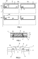
- the figure 1 thus illustrates a partial view of a carrier sheet 1 of a plurality of antenna circuits.
- Each circuit CA 1 , CA 2 , etc. comprises an antenna A wired technology whose two ends are each connected to a respective contact area c1, c2.
- Each antenna is arranged in a determined pattern, inside a dematerialized surface S which corresponds to the contours of the card body, when it is cut.
- the process is repeated until all the antennas provided on the support sheet are made.
- a microcircuit module M is fixed on a support sheet 1 of an antenna A.
- the two antenna ends, E1 and E2 are each connected to a respective contact, c1, c2, of module M.
- the support sheet is inserted into the thickness of the card 2, in the example by a rolling operation with other layers L1, L2, L3. This can also be done by molding.
- the module M can be fixed upside down, with the pads c1, c2 coming over the antenna ends (flip-chip technology). It is also possible to mount a microcircuit directly on the contact pads, for example in flip chip technology.
- the module or the microcircuit is fixed on the support sheet in a remote position of the contact pads c1 and c2 connected to the antenna ends.
- the support sheet further comprises connection tracks between the contact pads c1, c2 and the connection pads of the module or other contact pads connected to the module or electronic circuit. These tracks can be made in wired technology, or by metal etching, as the contact pads.
- the module M is embedded in the card, with external contact pads X flush on the surface of the card.
- the contact pads c1, c2 are typically etched metal pads on which are welded the ends E1, E2 of the antenna A.
- the antenna A is inserted at least in the part of the loops, in the material of the support sheet. This can be done in a known manner by an ultrasound technique.
- the inserting operation can take place before cutting, or after, individually on each unit card.
- the antenna formed by this method may further be at least partly inserted into the thickness of the support sheet, if it is made of plastic, as illustrated on the Figures 2 and 3 typically by ultrasonic means integrated into the head. In practice at least the antenna loops are thus inserted into the thickness of the support sheet.
- the method further includes checking each antenna circuit connected to its microcircuit. If the microcircuit is integrated in the card before the cutting operation, this verification can be done following a collective verification process.
- this collective verification process the support sheet 1 of the antenna circuits and microcircuits, or the card body plate, with insertion of microcircuit modules, is placed on a machine comprising several readers, each reader being positioned opposite an antenna of an antenna circuit, allowing this reader to communicate with the corresponding microcircuit via the antenna circuit.
- the reader's own antenna is typically glued or very close to the antenna circuit being tested.
- the machine is a table having on the surface the antenna of the readers, positioned to correspond to the positions of the antennas on the support sheet or in the plate. The machine then tests the operation of each microcircuit connected to its antenna circuit.
- the machine checks for each microcircuit, that when a reader initiates a short-range wireless communication, or contactless, the microcircuit can respond, which means that it is properly tele-powered. In addition, it can be verified that the answer on initialization ATS ( "Answer To Select" ) returned by the microcircuit is valid.
- the object of the invention is to improve the method of mass production of contactless or dual microcircuit cards, which uses a method for manufacturing antennas in wired technology.
- the invention therefore relates to a method of mass manufacturing electronic devices comprising an antenna and at least one microcircuit connected to said antenna, enabling wireless communications, the method comprising a step of manufacturing a plurality of planar antennas in technology. wired on the same support, characterized in that at least two antennas on said support are formed in a continuous process of unwinding the same wire, without cutting.
- the fixing of the wire in the support at a first point for a first antenna, the fixing of the wire in the support at a first point, the passage of the wire on the location of a first contact area to the microcircuit, the unwinding of the wire of so as to form one or more loops in said surface, passing the wire on the location of a second contact area to the microcircuit, fixing the wire in the support at a second point after said location of the second contact, then the unwinding wire to the first point of attachment of a subsequent antenna on said support.
- the antennas are each made inside a corresponding dematerialized surface on said support, the pattern formed by the wire in each of said surfaces being identical for each antenna.
- the invention also relates to an antenna circuit support, and portable electronic devices, in particular non-contact or dual cards, or RFID circuits, obtained according to this method.
- the invention also relates to an antenna circuit for wireless communications, formed on the surface of a support, said circuit comprising an antenna made of wire technology and comprising one or more loops of a wire between two ends of said wire, and two contact pads connected to the antenna, characterized in that the two ends of said wire are located on a respective edge of said support, and each of the connections to said contact pads is made at one or more points of the wire located between a respective end and said loop.
- an antenna circuit makes it possible to implement a method according to the invention, which makes it possible to produce it at a reduced cost.
- FIG. figure 4 A method of manufacturing a support 1 of a plurality of antenna circuits CA i according to the invention is illustrated in FIG. figure 4 , which shows the support obtained.
- the support is a support sheet, that is to say a thin object, adapted for example to the manufacture of ISO 7816 format cards.
- the antennas A on the support sheet are formed in a continuous process of unfolding the same wire F, without cutting.
- Steps b1 to e1 are repeated until reaching the second point of attachment of the last antenna made.
- step a1 is preceded by a preliminary step in which the tool 100 is positioned on the support sheet, on one edge, and the head moved to unroll the wire to the first attachment point of the first antenna.
- the antennas made are all identical.
- the cutting tool is integrated with the head 100.
- the cutting is possible only when the wire is oriented in a fixed direction, for example downwards, as illustrated in FIG. figure 4 .
- step f1 the formation of a loop F3 after the fixing point F2, which allows the cutting of the wire.
- the wire F is thus unrolled continuously from the beginning of the first antenna to the end of the last antenna made on the support sheet 1.
- the wire can be cut after making a first antenna group.
- the wire can be cut at the end of each line of antennas if they are made per line, or each column of antennas, if they are made per column.
- Step h of the state of the art described above moving the antenna in the high position between each antenna is replaced by step e1, of substantially the same duration, typically 0.5 seconds per antenna.
- the support sheet 1 is placed on a machine with a table comprising several readers.
- the sheet is positioned so that for each antenna A of the sheet, the antenna of a reader is glued or very close to this antenna A.
- the machine tests the operation of each drive pair, module M and antenna circuit CA i .
- the machine checks for each module M, that when a reader initializes the communication with this module, then this module responds with a response on initialization ATS, meaning that the module is properly powered.
- the machine can also verify that the content of the ATS response is valid.
- the collective test is carried out after the contact pads have been formed on the support sheet, before or after the antennas, and the soldered antenna wire, at one or more points, on each of the contact pads. , and that the antenna is connected to the microcircuit, or that the contact pads are directly pads of the microcircuit (or a module incorporating the microcircuit), or that the contact pads are connected to these pads, or by tracks performed on the same support sheet, possibly in wired technology, in the case of a microcircuit fixed on the support sheet but offset with respect to the locations of the ranges, c1, c2, or by inserting a module.
- the invention that has just been described makes it possible to optimize the method for the mass production of non-contact or dual microcircuit cards. Even applying it only in groups of antennas of the support sheet, one gains in manufacturing time. It suffices to make at least two successive antennas with the same wire continuously.
- the Figures 5 and 6 illustrate two embodiments of the wire portion connecting the second attachment point of a first antenna to the first attachment point of a subsequent antenna.
- this portion is made substantially midway between the parts of the loops of the first antenna which are parallel thereto. In this way the capacitance between this portion of wire and the first antenna is minimal and does not affect the resonant frequency of the assembly formed by the antenna circuit and the module connected thereto.
- this portion t is made substantially close to the parts of the loops of the first antenna which are parallel thereto.
- this portion of wire we create a passive loop, with a capacity between this portion of wire and the first antenna, which enters in determining the resonant frequency of the assembly formed by the antenna circuit and the module connected thereto.
- This variant makes it possible to improve the quality factor of the antennas A by increasing the capacitive portion compared with the inductive portion of the resonant circuit (antenna circuit connected to the module).
- the figure 7 illustrates another alternative embodiment of the invention by which, for a plastic support sheet, at least the antenna loops are inserted at least partially, that is to say at least at certain points, into the thickness of the support sheet, typically using the ultrasonic means integrated in the head of the antenna wire forming tool, while the portion t connecting two antennas successively made on the sheet is simply deposited on the surface, without being fixed thereon / inserted.
- the invention is applicable to the production of all types of contactless or dual cards, including cards in ID-1 format (credit card format), or smaller cards, such as for example format cards. ID-000 (SIM cards), and antennas of all sizes and loop patterns, especially for ID-1 format cards, ID-1 format antennas as shown on the figure 4 , or half-ID-1 as shown on the figure 1 . It is also applicable to any format of support sheet, for example a format making it possible to produce 3 * 8, 6 * 6, or 7 * 8 antennas, and any diameter of wire for example 80 ⁇ m, 112 ⁇ m, 130 ⁇ m, or other .
- the invention can be applied to any portable electronic device allowing wireless (non-contact) communications, such as, for example, RFID tags.
Landscapes
- Engineering & Computer Science (AREA)
- Computer Hardware Design (AREA)
- Microelectronics & Electronic Packaging (AREA)
- Physics & Mathematics (AREA)
- General Physics & Mathematics (AREA)
- Theoretical Computer Science (AREA)
- Computer Networks & Wireless Communication (AREA)
- Credit Cards Or The Like (AREA)
- Near-Field Transmission Systems (AREA)
Applications Claiming Priority (1)
| Application Number | Priority Date | Filing Date | Title |
|---|---|---|---|
| FR0858466A FR2939935B1 (fr) | 2008-12-11 | 2008-12-11 | Procede de fabrication de masse de dispositifs electroniques portables permettant des communications sans contact. |
Publications (3)
| Publication Number | Publication Date |
|---|---|
| EP2196951A2 true EP2196951A2 (de) | 2010-06-16 |
| EP2196951A3 EP2196951A3 (de) | 2013-04-03 |
| EP2196951B1 EP2196951B1 (de) | 2016-02-24 |
Family
ID=40584701
Family Applications (1)
| Application Number | Title | Priority Date | Filing Date |
|---|---|---|---|
| EP09173438.4A Not-in-force EP2196951B1 (de) | 2008-12-11 | 2009-10-19 | Verfahren zur Massenproduktion von tragbaren elektronischen Geräten zur kontaktlosen Kommunikation |
Country Status (2)
| Country | Link |
|---|---|
| EP (1) | EP2196951B1 (de) |
| FR (1) | FR2939935B1 (de) |
Citations (3)
| Publication number | Priority date | Publication date | Assignee | Title |
|---|---|---|---|---|
| US6088230A (en) | 1994-03-28 | 2000-07-11 | Finn; David | Procedure for producing a chip mounting board and chip-mounting board thus produced |
| US6233818B1 (en) | 1996-02-12 | 2001-05-22 | David Finn | Method and device for bonding a wire conductor |
| US6626364B2 (en) | 2001-10-09 | 2003-09-30 | Tandis, Inc. | High speed system for embedding wire antennas in an array of smart cards |
Family Cites Families (2)
| Publication number | Priority date | Publication date | Assignee | Title |
|---|---|---|---|---|
| US6628240B2 (en) * | 2000-11-08 | 2003-09-30 | American Pacific Technology | Method and apparatus for rapid staking of antennae in smart card manufacture |
| US7913917B2 (en) * | 2006-07-24 | 2011-03-29 | Textilma Ag | RFID tag |
-
2008
- 2008-12-11 FR FR0858466A patent/FR2939935B1/fr not_active Expired - Fee Related
-
2009
- 2009-10-19 EP EP09173438.4A patent/EP2196951B1/de not_active Not-in-force
Patent Citations (3)
| Publication number | Priority date | Publication date | Assignee | Title |
|---|---|---|---|---|
| US6088230A (en) | 1994-03-28 | 2000-07-11 | Finn; David | Procedure for producing a chip mounting board and chip-mounting board thus produced |
| US6233818B1 (en) | 1996-02-12 | 2001-05-22 | David Finn | Method and device for bonding a wire conductor |
| US6626364B2 (en) | 2001-10-09 | 2003-09-30 | Tandis, Inc. | High speed system for embedding wire antennas in an array of smart cards |
Also Published As
| Publication number | Publication date |
|---|---|
| EP2196951B1 (de) | 2016-02-24 |
| EP2196951A3 (de) | 2013-04-03 |
| FR2939935B1 (fr) | 2010-12-17 |
| FR2939935A1 (fr) | 2010-06-18 |
Similar Documents
| Publication | Publication Date | Title |
|---|---|---|
| EP2158604B1 (de) | Zusammenbau von hochfrequenzchips | |
| EP1118960B1 (de) | Kontaktloser elektronischer Modul für eine Karte oder ein Etikett | |
| FR2821691A1 (fr) | Procede de realisation d'une carte a ci a double interface et carte realisee suivant un tel procede | |
| FR2830986A1 (fr) | Procede, appareil, systeme et article pour la formation d'antennes de carte a memoire | |
| EP3304432B1 (de) | Funkantennenschaltkreis mit gegenseitigen eingebetteten induktoren | |
| WO2017102667A1 (fr) | Dispositif radiofrequence a circuit lc ajustable comprenant un module electrique et/ou electronique | |
| FR2953046A1 (fr) | Corps de carte a microcircuit formant support de deux etiquettes electroniques | |
| WO2004107260A2 (fr) | Procede de fabrication d’un ticket a puce sans contact | |
| WO2008080876A1 (fr) | Procede de realisation de dispositifs de communication radiofrequence avec ou sans interrupteur de fonctionnement et dispositifs obtenus | |
| EP2545503B1 (de) | Elektronische vorrichtung mit einem chip und herstellungsverfahren mittels spulen | |
| EP2196951B1 (de) | Verfahren zur Massenproduktion von tragbaren elektronischen Geräten zur kontaktlosen Kommunikation | |
| EP1989664B1 (de) | Herstellungsverfahren von chipkarten | |
| WO2010058109A2 (fr) | Procede de fabrication d'objets portatifs sans contact avec pont dielectrique et objets portatifs | |
| EP3230926B1 (de) | Herstellungsverfahren einer funkvorrichtung, die eine mit einer drahtkondensatorplatte verbundene antenne umfasst | |
| EP2915104B1 (de) | Verfahren zur herstellung einer anschlussvorrichtung für das modul einer smart card, durch das verfahren erhaltene anschlussvorrichtung und modul mit smart card anschlussvorrichtung | |
| EP1724712A1 (de) | Micromodul, speziell für eine Smart Card | |
| FR2999753A1 (fr) | Procede de fabrication par lamination en continu de cartes a microcircuit du type a contact | |
| WO2011023570A1 (fr) | Procede de realisation d'un dispositif comprenant un circuit radiofrequence, et dispositif obtenu | |
| EP2089836B1 (de) | Mikroschaltplatte mit offset-antenne | |
| EP2043027A1 (de) | Verfahren zur Herstellung einer Transponderantenne auf einem Substrat durch Verbindung von Teilen der Antennenwindungen und entsprechende Antenne | |
| WO2013034759A1 (fr) | Dispositif électronique à puce et procédé de fabrication par bobines | |
| FR2997783A1 (fr) | Procede et dispositif de fabrication d'une antenne | |
| EP2053545A1 (de) | Verfahren zur Herstellung von Funkkommunikationsvorrichtungen, die einen vorübergehend kurzgeschlossenen Schalter umfassen | |
| EP2293227A1 (de) | Vorrichtung mit einer Relais-Antenne, zugehörige Radiofrequenzvorrichtung und zugehöriges Verfahren | |
| EP2525305A1 (de) | Fadenkondensator, insbesondere für Funkschaltkreis, und diesen umfassende Vorrichtung |
Legal Events
| Date | Code | Title | Description |
|---|---|---|---|
| PUAI | Public reference made under article 153(3) epc to a published international application that has entered the european phase |
Free format text: ORIGINAL CODE: 0009012 |
|
| AK | Designated contracting states |
Kind code of ref document: A2 Designated state(s): AT BE BG CH CY CZ DE DK EE ES FI FR GB GR HR HU IE IS IT LI LT LU LV MC MK MT NL NO PL PT RO SE SI SK SM TR |
|
| AX | Request for extension of the european patent |
Extension state: AL BA RS |
|
| PUAL | Search report despatched |
Free format text: ORIGINAL CODE: 0009013 |
|
| AK | Designated contracting states |
Kind code of ref document: A3 Designated state(s): AT BE BG CH CY CZ DE DK EE ES FI FR GB GR HR HU IE IS IT LI LT LU LV MC MK MT NL NO PL PT RO SE SI SK SM TR |
|
| AX | Request for extension of the european patent |
Extension state: AL BA RS |
|
| RIC1 | Information provided on ipc code assigned before grant |
Ipc: G06K 19/077 20060101AFI20130225BHEP |
|
| 17P | Request for examination filed |
Effective date: 20130524 |
|
| RBV | Designated contracting states (corrected) |
Designated state(s): AT BE BG CH CY CZ DE DK EE ES FI FR GB GR HR HU IE IS IT LI LT LU LV MC MK MT NL NO PL PT RO SE SI SK SM TR |
|
| 17Q | First examination report despatched |
Effective date: 20140117 |
|
| GRAP | Despatch of communication of intention to grant a patent |
Free format text: ORIGINAL CODE: EPIDOSNIGR1 |
|
| INTG | Intention to grant announced |
Effective date: 20151005 |
|
| GRAS | Grant fee paid |
Free format text: ORIGINAL CODE: EPIDOSNIGR3 |
|
| GRAA | (expected) grant |
Free format text: ORIGINAL CODE: 0009210 |
|
| AK | Designated contracting states |
Kind code of ref document: B1 Designated state(s): AT BE BG CH CY CZ DE DK EE ES FI FR GB GR HR HU IE IS IT LI LT LU LV MC MK MT NL NO PL PT RO SE SI SK SM TR |
|
| REG | Reference to a national code |
Ref country code: GB Ref legal event code: FG4D Free format text: NOT ENGLISH |
|
| REG | Reference to a national code |
Ref country code: CH Ref legal event code: EP |
|
| REG | Reference to a national code |
Ref country code: AT Ref legal event code: REF Ref document number: 777071 Country of ref document: AT Kind code of ref document: T Effective date: 20160315 |
|
| REG | Reference to a national code |
Ref country code: IE Ref legal event code: FG4D Free format text: LANGUAGE OF EP DOCUMENT: FRENCH |
|
| REG | Reference to a national code |
Ref country code: DE Ref legal event code: R096 Ref document number: 602009036438 Country of ref document: DE |
|
| REG | Reference to a national code |
Ref country code: LT Ref legal event code: MG4D |
|
| REG | Reference to a national code |
Ref country code: NL Ref legal event code: MP Effective date: 20160224 |
|
| REG | Reference to a national code |
Ref country code: AT Ref legal event code: MK05 Ref document number: 777071 Country of ref document: AT Kind code of ref document: T Effective date: 20160224 |
|
| PG25 | Lapsed in a contracting state [announced via postgrant information from national office to epo] |
Ref country code: GR Free format text: LAPSE BECAUSE OF FAILURE TO SUBMIT A TRANSLATION OF THE DESCRIPTION OR TO PAY THE FEE WITHIN THE PRESCRIBED TIME-LIMIT Effective date: 20160525 Ref country code: HR Free format text: LAPSE BECAUSE OF FAILURE TO SUBMIT A TRANSLATION OF THE DESCRIPTION OR TO PAY THE FEE WITHIN THE PRESCRIBED TIME-LIMIT Effective date: 20160224 Ref country code: NO Free format text: LAPSE BECAUSE OF FAILURE TO SUBMIT A TRANSLATION OF THE DESCRIPTION OR TO PAY THE FEE WITHIN THE PRESCRIBED TIME-LIMIT Effective date: 20160524 Ref country code: ES Free format text: LAPSE BECAUSE OF FAILURE TO SUBMIT A TRANSLATION OF THE DESCRIPTION OR TO PAY THE FEE WITHIN THE PRESCRIBED TIME-LIMIT Effective date: 20160224 Ref country code: IT Free format text: LAPSE BECAUSE OF FAILURE TO SUBMIT A TRANSLATION OF THE DESCRIPTION OR TO PAY THE FEE WITHIN THE PRESCRIBED TIME-LIMIT Effective date: 20160224 Ref country code: FI Free format text: LAPSE BECAUSE OF FAILURE TO SUBMIT A TRANSLATION OF THE DESCRIPTION OR TO PAY THE FEE WITHIN THE PRESCRIBED TIME-LIMIT Effective date: 20160224 |
|
| PG25 | Lapsed in a contracting state [announced via postgrant information from national office to epo] |
Ref country code: NL Free format text: LAPSE BECAUSE OF FAILURE TO SUBMIT A TRANSLATION OF THE DESCRIPTION OR TO PAY THE FEE WITHIN THE PRESCRIBED TIME-LIMIT Effective date: 20160224 Ref country code: LV Free format text: LAPSE BECAUSE OF FAILURE TO SUBMIT A TRANSLATION OF THE DESCRIPTION OR TO PAY THE FEE WITHIN THE PRESCRIBED TIME-LIMIT Effective date: 20160224 Ref country code: PL Free format text: LAPSE BECAUSE OF FAILURE TO SUBMIT A TRANSLATION OF THE DESCRIPTION OR TO PAY THE FEE WITHIN THE PRESCRIBED TIME-LIMIT Effective date: 20160224 Ref country code: LT Free format text: LAPSE BECAUSE OF FAILURE TO SUBMIT A TRANSLATION OF THE DESCRIPTION OR TO PAY THE FEE WITHIN THE PRESCRIBED TIME-LIMIT Effective date: 20160224 Ref country code: AT Free format text: LAPSE BECAUSE OF FAILURE TO SUBMIT A TRANSLATION OF THE DESCRIPTION OR TO PAY THE FEE WITHIN THE PRESCRIBED TIME-LIMIT Effective date: 20160224 Ref country code: SE Free format text: LAPSE BECAUSE OF FAILURE TO SUBMIT A TRANSLATION OF THE DESCRIPTION OR TO PAY THE FEE WITHIN THE PRESCRIBED TIME-LIMIT Effective date: 20160224 Ref country code: PT Free format text: LAPSE BECAUSE OF FAILURE TO SUBMIT A TRANSLATION OF THE DESCRIPTION OR TO PAY THE FEE WITHIN THE PRESCRIBED TIME-LIMIT Effective date: 20160624 |
|
| REG | Reference to a national code |
Ref country code: FR Ref legal event code: PLFP Year of fee payment: 8 |
|
| PG25 | Lapsed in a contracting state [announced via postgrant information from national office to epo] |
Ref country code: DK Free format text: LAPSE BECAUSE OF FAILURE TO SUBMIT A TRANSLATION OF THE DESCRIPTION OR TO PAY THE FEE WITHIN THE PRESCRIBED TIME-LIMIT Effective date: 20160224 Ref country code: EE Free format text: LAPSE BECAUSE OF FAILURE TO SUBMIT A TRANSLATION OF THE DESCRIPTION OR TO PAY THE FEE WITHIN THE PRESCRIBED TIME-LIMIT Effective date: 20160224 |
|
| REG | Reference to a national code |
Ref country code: DE Ref legal event code: R097 Ref document number: 602009036438 Country of ref document: DE |
|
| PG25 | Lapsed in a contracting state [announced via postgrant information from national office to epo] |
Ref country code: RO Free format text: LAPSE BECAUSE OF FAILURE TO SUBMIT A TRANSLATION OF THE DESCRIPTION OR TO PAY THE FEE WITHIN THE PRESCRIBED TIME-LIMIT Effective date: 20160224 Ref country code: SK Free format text: LAPSE BECAUSE OF FAILURE TO SUBMIT A TRANSLATION OF THE DESCRIPTION OR TO PAY THE FEE WITHIN THE PRESCRIBED TIME-LIMIT Effective date: 20160224 Ref country code: SM Free format text: LAPSE BECAUSE OF FAILURE TO SUBMIT A TRANSLATION OF THE DESCRIPTION OR TO PAY THE FEE WITHIN THE PRESCRIBED TIME-LIMIT Effective date: 20160224 Ref country code: CZ Free format text: LAPSE BECAUSE OF FAILURE TO SUBMIT A TRANSLATION OF THE DESCRIPTION OR TO PAY THE FEE WITHIN THE PRESCRIBED TIME-LIMIT Effective date: 20160224 |
|
| PLBE | No opposition filed within time limit |
Free format text: ORIGINAL CODE: 0009261 |
|
| STAA | Information on the status of an ep patent application or granted ep patent |
Free format text: STATUS: NO OPPOSITION FILED WITHIN TIME LIMIT |
|
| 26N | No opposition filed |
Effective date: 20161125 |
|
| PG25 | Lapsed in a contracting state [announced via postgrant information from national office to epo] |
Ref country code: BG Free format text: LAPSE BECAUSE OF FAILURE TO SUBMIT A TRANSLATION OF THE DESCRIPTION OR TO PAY THE FEE WITHIN THE PRESCRIBED TIME-LIMIT Effective date: 20160524 Ref country code: SI Free format text: LAPSE BECAUSE OF FAILURE TO SUBMIT A TRANSLATION OF THE DESCRIPTION OR TO PAY THE FEE WITHIN THE PRESCRIBED TIME-LIMIT Effective date: 20160224 Ref country code: BE Free format text: LAPSE BECAUSE OF NON-PAYMENT OF DUE FEES Effective date: 20161031 |
|
| REG | Reference to a national code |
Ref country code: DE Ref legal event code: R119 Ref document number: 602009036438 Country of ref document: DE |
|
| REG | Reference to a national code |
Ref country code: CH Ref legal event code: PL |
|
| GBPC | Gb: european patent ceased through non-payment of renewal fee |
Effective date: 20161019 |
|
| REG | Reference to a national code |
Ref country code: IE Ref legal event code: MM4A |
|
| PG25 | Lapsed in a contracting state [announced via postgrant information from national office to epo] |
Ref country code: GB Free format text: LAPSE BECAUSE OF NON-PAYMENT OF DUE FEES Effective date: 20161019 Ref country code: LI Free format text: LAPSE BECAUSE OF NON-PAYMENT OF DUE FEES Effective date: 20161031 Ref country code: CH Free format text: LAPSE BECAUSE OF NON-PAYMENT OF DUE FEES Effective date: 20161031 Ref country code: DE Free format text: LAPSE BECAUSE OF NON-PAYMENT OF DUE FEES Effective date: 20170503 |
|
| PG25 | Lapsed in a contracting state [announced via postgrant information from national office to epo] |
Ref country code: LU Free format text: LAPSE BECAUSE OF NON-PAYMENT OF DUE FEES Effective date: 20161019 |
|
| REG | Reference to a national code |
Ref country code: FR Ref legal event code: PLFP Year of fee payment: 9 |
|
| PG25 | Lapsed in a contracting state [announced via postgrant information from national office to epo] |
Ref country code: IE Free format text: LAPSE BECAUSE OF NON-PAYMENT OF DUE FEES Effective date: 20161019 |
|
| REG | Reference to a national code |
Ref country code: BE Ref legal event code: MM Effective date: 20161031 |
|
| PG25 | Lapsed in a contracting state [announced via postgrant information from national office to epo] |
Ref country code: HU Free format text: LAPSE BECAUSE OF FAILURE TO SUBMIT A TRANSLATION OF THE DESCRIPTION OR TO PAY THE FEE WITHIN THE PRESCRIBED TIME-LIMIT; INVALID AB INITIO Effective date: 20091019 Ref country code: CY Free format text: LAPSE BECAUSE OF FAILURE TO SUBMIT A TRANSLATION OF THE DESCRIPTION OR TO PAY THE FEE WITHIN THE PRESCRIBED TIME-LIMIT Effective date: 20160224 |
|
| PG25 | Lapsed in a contracting state [announced via postgrant information from national office to epo] |
Ref country code: MK Free format text: LAPSE BECAUSE OF FAILURE TO SUBMIT A TRANSLATION OF THE DESCRIPTION OR TO PAY THE FEE WITHIN THE PRESCRIBED TIME-LIMIT Effective date: 20160224 Ref country code: IS Free format text: LAPSE BECAUSE OF FAILURE TO SUBMIT A TRANSLATION OF THE DESCRIPTION OR TO PAY THE FEE WITHIN THE PRESCRIBED TIME-LIMIT Effective date: 20160224 Ref country code: MC Free format text: LAPSE BECAUSE OF FAILURE TO SUBMIT A TRANSLATION OF THE DESCRIPTION OR TO PAY THE FEE WITHIN THE PRESCRIBED TIME-LIMIT Effective date: 20160224 Ref country code: MT Free format text: LAPSE BECAUSE OF FAILURE TO SUBMIT A TRANSLATION OF THE DESCRIPTION OR TO PAY THE FEE WITHIN THE PRESCRIBED TIME-LIMIT Effective date: 20160224 Ref country code: TR Free format text: LAPSE BECAUSE OF FAILURE TO SUBMIT A TRANSLATION OF THE DESCRIPTION OR TO PAY THE FEE WITHIN THE PRESCRIBED TIME-LIMIT Effective date: 20160224 |
|
| REG | Reference to a national code |
Ref country code: FR Ref legal event code: PLFP Year of fee payment: 10 |
|
| PGFP | Annual fee paid to national office [announced via postgrant information from national office to epo] |
Ref country code: FR Payment date: 20190919 Year of fee payment: 11 |
|
| PG25 | Lapsed in a contracting state [announced via postgrant information from national office to epo] |
Ref country code: FR Free format text: LAPSE BECAUSE OF NON-PAYMENT OF DUE FEES Effective date: 20201031 |