EP2197246A2 - Beleuchtungsvorrichtung und Beleuchtungsbefestigung damit - Google Patents
Beleuchtungsvorrichtung und Beleuchtungsbefestigung damit Download PDFInfo
- Publication number
- EP2197246A2 EP2197246A2 EP09014952A EP09014952A EP2197246A2 EP 2197246 A2 EP2197246 A2 EP 2197246A2 EP 09014952 A EP09014952 A EP 09014952A EP 09014952 A EP09014952 A EP 09014952A EP 2197246 A2 EP2197246 A2 EP 2197246A2
- Authority
- EP
- European Patent Office
- Prior art keywords
- lamp
- lighting device
- fluorescent
- voltage
- led lamp
- Prior art date
- Legal status (The legal status is an assumption and is not a legal conclusion. Google has not performed a legal analysis and makes no representation as to the accuracy of the status listed.)
- Withdrawn
Links
- 238000005286 illumination Methods 0.000 title claims abstract description 14
- 239000003990 capacitor Substances 0.000 description 50
- 238000001514 detection method Methods 0.000 description 30
- 238000010586 diagram Methods 0.000 description 12
- 238000009499 grossing Methods 0.000 description 3
- 238000000034 method Methods 0.000 description 2
- 230000001172 regenerating effect Effects 0.000 description 2
- 240000004050 Pentaglottis sempervirens Species 0.000 description 1
- 235000004522 Pentaglottis sempervirens Nutrition 0.000 description 1
- 239000000470 constituent Substances 0.000 description 1
- 238000007796 conventional method Methods 0.000 description 1
- 230000000694 effects Effects 0.000 description 1
- 239000000758 substrate Substances 0.000 description 1
Images




Classifications
-
- H—ELECTRICITY
- H05—ELECTRIC TECHNIQUES NOT OTHERWISE PROVIDED FOR
- H05B—ELECTRIC HEATING; ELECTRIC LIGHT SOURCES NOT OTHERWISE PROVIDED FOR; CIRCUIT ARRANGEMENTS FOR ELECTRIC LIGHT SOURCES, IN GENERAL
- H05B45/00—Circuit arrangements for operating light-emitting diodes [LED]
- H05B45/40—Details of LED load circuits
- H05B45/44—Details of LED load circuits with an active control inside an LED matrix
-
- H—ELECTRICITY
- H05—ELECTRIC TECHNIQUES NOT OTHERWISE PROVIDED FOR
- H05B—ELECTRIC HEATING; ELECTRIC LIGHT SOURCES NOT OTHERWISE PROVIDED FOR; CIRCUIT ARRANGEMENTS FOR ELECTRIC LIGHT SOURCES, IN GENERAL
- H05B45/00—Circuit arrangements for operating light-emitting diodes [LED]
- H05B45/30—Driver circuits
- H05B45/37—Converter circuits
- H05B45/3725—Switched mode power supply [SMPS]
- H05B45/375—Switched mode power supply [SMPS] using buck topology
-
- H—ELECTRICITY
- H05—ELECTRIC TECHNIQUES NOT OTHERWISE PROVIDED FOR
- H05B—ELECTRIC HEATING; ELECTRIC LIGHT SOURCES NOT OTHERWISE PROVIDED FOR; CIRCUIT ARRANGEMENTS FOR ELECTRIC LIGHT SOURCES, IN GENERAL
- H05B45/00—Circuit arrangements for operating light-emitting diodes [LED]
- H05B45/30—Driver circuits
- H05B45/37—Converter circuits
- H05B45/3725—Switched mode power supply [SMPS]
- H05B45/38—Switched mode power supply [SMPS] using boost topology
-
- H—ELECTRICITY
- H05—ELECTRIC TECHNIQUES NOT OTHERWISE PROVIDED FOR
- H05B—ELECTRIC HEATING; ELECTRIC LIGHT SOURCES NOT OTHERWISE PROVIDED FOR; CIRCUIT ARRANGEMENTS FOR ELECTRIC LIGHT SOURCES, IN GENERAL
- H05B45/00—Circuit arrangements for operating light-emitting diodes [LED]
- H05B45/30—Driver circuits
- H05B45/37—Converter circuits
- H05B45/3725—Switched mode power supply [SMPS]
- H05B45/39—Circuits containing inverter bridges
-
- Y—GENERAL TAGGING OF NEW TECHNOLOGICAL DEVELOPMENTS; GENERAL TAGGING OF CROSS-SECTIONAL TECHNOLOGIES SPANNING OVER SEVERAL SECTIONS OF THE IPC; TECHNICAL SUBJECTS COVERED BY FORMER USPC CROSS-REFERENCE ART COLLECTIONS [XRACs] AND DIGESTS
- Y02—TECHNOLOGIES OR APPLICATIONS FOR MITIGATION OR ADAPTATION AGAINST CLIMATE CHANGE
- Y02B—CLIMATE CHANGE MITIGATION TECHNOLOGIES RELATED TO BUILDINGS, e.g. HOUSING, HOUSE APPLIANCES OR RELATED END-USER APPLICATIONS
- Y02B20/00—Energy efficient lighting technologies, e.g. halogen lamps or gas discharge lamps
- Y02B20/30—Semiconductor lamps, e.g. solid state lamps [SSL] light emitting diodes [LED] or organic LED [OLED]
Definitions
- the present invention relates to a lighting device lighting a fluorescent lamp or a fluorescent LED lamp and a illumination fixture using the same.
- Fig. 2 shows a bird's-eye view of a fluorescent LED lamp.
- Fig. 3 is an equivalent circuit diagram.
- the fluorescent LED lamp is configured so that a plurality of LEDs mounted on a substrate is connected between lamp electrodes.
- the fluorescent LED lamp is on the market as one for realizing power saving with a long life by attaching not a fluorescent lamp but the fluorescent LED lamp to a conventional fluorescent illumination fixture.
- the fluorescent illumination fixture to which the fluorescent LED lamp is attached is conventionally often incompatible with an inverter illumination fixture.
- Patent Document 1 Japanese Unexamined Patent Publication No. 2003-168580 discloses a lighting device intended at cost reduction by sharing a high frequency lighting circuit among fluorescent lamps of different types. With a technique of the Patent Document, a lamp current of each fluorescent lamp is detected, a type of each fluorescent lamp is discriminated according to a difference in the lamp current, and power supplied to each fluorescent lamp is controlled based on a discrimination result. However, the technique is not intended to discriminate difference between the fluorescent lamp and the fluorescent LED lamp.
- incompatibility of the inverter illumination fixture with the fluorescent LED lamp is considered to result from a fact that a higher voltage than a rated lighting voltage is outputted to between lamp output terminals at the time of starting each fluorescent lamp and an excessive voltage is outputted to each fluorescent LED lamp to destroy each in the inverter illumination fixture.
- the present invention has been made in light of these respects. It is an object of the present invention to make it possible to light a fluorescent LED lamp in an illumination fixture using an inverter lighting device.
- a lighting device for lighting a fluorescent lamp with a high frequency including a function of detecting that a fluorescent LED lamp is attached to the lighting device, wherein a voltage suited for the fluorescent LED lamp is outputted if the function detects that the fluorescent LED lamp is attached to the lighting device.
- the lighting device includes a function of detecting that the fluorescent LED lamp is attached to the lighting device by applying an output voltage lower than a rated voltage of the fluorescent lamp to between lamp output terminals in a predetermined period after the lighting device is lighted on, wherein in the case where the function does not detect that the fluorescent LED lamp is attached to the lighting device in the predetermined period, the lighting device performs operations of preheating, starting and lighting suited for the fluorescent lamp.
- an output voltage applied to between the lamp output terminals in the predetermined period after the lighting device is lighted on is a direct-current voltage
- the function detects that the fluorescent LED lamp is attached to the lighting device by detecting that a current is applied to between the lamp output terminals as a result of application of the DC voltage
- the output voltage applied to between the lamp output terminals in the predetermined period after the lighting device is lighted on is a high-frequency voltage
- the function detects that the fluorescent LED lamp is attached to the lighting device by detecting that a current equal to or higher than a predetermined current is applied to between the lamp output terminals as a result of application of the high-frequency voltage.
- an illumination fixture including the lighting device according to any one of the first to fourth aspects of the present invention.
- the lighting device includes the function of detecting the fluorescent LED lamp and outputs the voltage suited for the fluorescent LED lamp if the function detects the fluorescent LED lamp, whereby it is possible to light not only the fluorescent lamp but also the fluorescent LED lamp in the fluorescent illumination fixture using the inverter lighting device.
- FIG. 1 is a block diagram showing a schematic configuration of a first embodiment of the present invention.
- a lighting device 1 includes a high-frequency power source part 2, a direct-current (DC) power source part 3, and a load determination part 4.
- the high-frequency power source part 2 functions to output a high-frequency voltage to between lamp output terminals a and c.
- the DC power source part 3 functions to output a DC voltage to between the lamp output terminals a and c.
- Switching means 5 selects one of the high-frequency power source part 2 and the DC power source part 3 according to a determination result of a load determination part 4.
- the load determination part 4 functions to activate/deactivate the high-frequency power source part 2 and the DC power source part 3 and to adjust an output of the high-frequency power source part 2 and the DC power source part 3.
- the load determination part 4 selects not the high-frequency power source part 2 but the DC power source part 3, and outputs a low DC voltage to between the lamp output terminals a and c.
- current detection means 6 functions to determine whether a load connected to between the lamp output terminals a and c is a fluorescent lamp 7 (see Fig. 1 ) or a fluorescent LED lamp 8 (see Figs. 2 and 3 ) by determining whether or not a current is applied to between the lamp output terminals a and c.
- the fluorescent lamp 7 includes filaments f1 and f2 on both ends of a discharge tube, respectively.
- One filament f1 is connected to between lamp output terminals a and b whereas the other filament f2 is connected to between lamp output terminals c and d.
- the fluorescent LED lamp 8 is configured to accommodate therein a plurality of LEDs generally identical in shape to the fluorescent lamp 7 and a lighting circuit 9.
- a serial circuit of the lighting circuit 9 and the LEDs is connected to the lamp output terminals a to d via a bridge circuit including diodes D11 to D14 and a bridge circuit including diodes D21 to D24.
- the lighting circuit 9 may be a current-limiting resistor.
- Fig. 4 shows lighting waveforms when the fluorescent lamp 7 and the fluorescent LED lamp 8 are attached to the lighting device 1, respectively.
- Fig. 4(a) shows an instance in which the fluorescent lamp 7 is attached to the lighting device 1
- Fig. 4(b) shows an instance in which the fluorescent LED lamp 8 is attached thereto.
- a broken line indicates an envelope of a high-frequency voltage of Fig. 4(a) . It is understood that a high-frequency voltage is not applied to the fluorescent LED lamp 8 if the fluorescent LED lamp 8 is attached to the lighting device 1 differently from the instance in which the fluorescent lamp 7 is attached to the lighting device 1.
- a DC voltage lower than a rated voltage of the fluorescent lamp 7 is outputted to between the lamp output terminals a and c, in which period, a type of the lamp is determined.
- An equivalent circuit to the fluorescent LED lamp 8 is that as shown in Fig. 3 . Therefore, even the lower DC voltage than the rated voltage of the fluorescent lamp 7 is applied to between the lamp output terminals a and c, a current is applied thereto. If detecting this current, the current detection means 6 determines that the fluorescent LED lamp 8 is attached to the lighting device 1. Thereafter, a DC voltage higher than that applied in the predetermined period after the lighting device 1 is lighted on is outputted to between the lamp output terminals a and c, thereby lighting the fluorescent LED lamp 8 with a sufficient output.
- the load determination part 4 can detect the type of the lamp depending on whether or not a current is applied when the DC voltage is outputted.
- the load determination part 4 determines that the fluorescent lamp 7 is attached to the lighting device 1, the switching means 5 selects the high-frequency power source 2, and the lighting device 1 operates in a sequence of preheating, starting and lighting necessary to light the fluorescent lamp 7.
- the lighting device 1 is controlled to apply an enough preheat current to the filaments f1 and f2 of the fluorescent lamp 7 while keeping a voltage applied to between the both ends of the fluorescent lamp 7 lower than a starting voltage in a preheating period, to apply a voltage higher than the starting voltage to between the both ends of the fluorescent lamp 7 in a starting period, and to apply the rated voltage of the fluorescent lamp 7 to between the both ends of the fluorescent lamp 7 in a lighting period.
- Fig. 5 is a circuit diagram of a second embodiment of the present invention.
- the second embodiment is a specific example of a circuit realizing the operation in the first embodiment.
- a lighting device shown in Fig. 5 includes a DC power source part 11 and an inverter part 12.
- the DC power source part 11 is configured to include a rectifier DB rectifying full waves of an alternating-current (AC) power source Vs, a set-up chopper circuit that includes an inductor L1 connected to an output of this rectifier DB, a switching element Q1 and a diode D1, and an electrolytic capacitor C1 smoothing an output from the set-up chopper circuit.
- the DC power source part 11 supplies a DC voltage to the inverter part 12.
- the inverter part 12 is configured to include a serial circuit of switching elements Q2 and Q3 that constitute a half-bridge inverter, and a load circuit is connected to both ends of the switching element Q3.
- Reference symbols a, b, c, and d denote lamp output terminals, and a lighting voltage to be applied to a lamp is outputted to between the lamp output terminals a and c.
- a capacitor C2 is a resonance capacitor if a fluorescent lamp 7 is connected, and the capacitor C2 and an inductor L2 constitute a DC-cutting capacitor.
- a capacitor C3 is a DC-cutting capacitor. The capacitor C3 operates as the DC-cutting capacitor if the fluorescent lamp 7 is connected.
- a switching element Q5 serially connected to the capacitor C3 is turned off, whereby the capacitor C3 acts as the DC-cutting capacitor.
- a capacitor C4 is a smoothing capacitor.
- the capacitor C4 operates as a smoothing capacitor if the fluorescent LED lamp 8 is connected to the lamp output terminals.
- a switching element Q4 serially connected to the capacitor C4 is turned on, whereby the capacitor C4 as well as the inductor L2 is connected to both ends of the switching element Q3 and the capacitor C4 is used as an output capacitor if each LED of the fluorescent lamp 8 is lighted by an output from a set-down chopper. In this case, at the same time, the switching element Q5 is turned on to short the DC-cutting capacitor C3, thereby invalidating the DC-cutting capacitor C3.
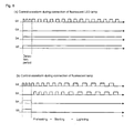
- Fig. 6 shows operation waveforms according to the present embodiment.
- Fig. 6(a) shows control signal waveforms of the switching elements Q2, Q3, Q4, and Q5 if the fluorescent LED lamp 8 is connected.
- Fig. 6(b) shows control signal waveforms of the switching elements Q2, Q3, Q4, and Q5 if the fluorescent lamp 7 is connected.
- a current flows in a route of the capacitor C1 ⁇ the switching element Q2 ⁇ the inductor L2 ⁇ the capacitor C4 ⁇ the switching element Q4 ⁇ the capacitor C1.
- a current is applied to the lamp and the capacitor C4 while accumulating energy in the inductor L2.
- a regenerative current flows in a route of the inductor L2 ⁇ the lamp (terminals a ⁇ c) ⁇ the switching element Q5 ⁇ the diode included in switching element Q3 ⁇ the inductor L2.
- a regenerative current flows in a route of the inductor L2 ⁇ the capacitor C4 ⁇ the switching element Q4 ⁇ the diode included in switching element Q3 ⁇ the inductor L2.
- the energy accumulated in the inductor L2 is emitted to the lamp and the capacitor C4.
- the fluorescent LED lamp 8 If it is detected that a current is applied to the lamp during the detection period, it is determined that the fluorescent LED lamp 8 is connected to between the lamp output terminals a and c. Further, frequencies for turning on and off the switching element Q2 are controlled to be appropriately lower so as to output a DC voltage suited for the fluorescent LED lamp 8.
- current detection means is not shown, it suffices to insert a current detection resistor somewhere in the route of flow of a lamp current. For example, the current detection resistor may detect a voltage drop due to a resistance between a drain and a source of the switching element Q5.
- the fluorescent lamp 7 is connected, then the fluorescent lamp 7 is not lighted by an output voltage from the set-down chopper, and a current is not eventually applied to between the lamp output terminals (a ⁇ c). If it is detected that the current does not flow in the predetermined period (detection period) after the lighting device is lighted on, then it is determined that the lamp is not the fluorescent LED lamp 8, and the lighting device performs an operation for lighting the fluorescent lamp 7.
- both the switching elements Q4 and Q5 are turned off, and the capacitor C4 of the set-down chopper is separated from the circuit, thereby turning the DC-cutting capacitor C3 into a state of being connected in series to the lamp output terminals.
- an operation for turning on or off the switching element Q3 complementarily with the switching element Q2 starts, thereby outputting a high-frequency output voltage to between the lamp output terminals a and c.
- Switching frequencies of the switching elements Q2 and Q3 are appropriately reduced in each of preheating, starting and lighting periods, and an appropriate high-frequency voltage is outputted to between the lamp output terminals a and c, thereby making it possible to eventually light the fluorescent lamp 7.
- the period for turning on or off only one of the switching elements Q2 and Q3 constituting the half-bridge inverter is set, thereby causing the lighting device to operate as the set-down chopper to be able to output the DC voltage to between the lamp output terminals a and c. Therefore, the switching element Q2 and the inductor L2 of the inverter can be also used as constituent elements of the set-down chopper, making cost reduction possible.
- Fig. 7 is a circuit diagram according to a third embodiment of the present invention.
- the third embodiment is another specific example of a circuit realizing the operation in the first embodiment.
- a lighting device shown in Fig. 7 includes a DC power source part 11 and an inverter part 12.
- the DC power source part 11 is configured similarly to that shown in Fig. 5 and supplies a DC voltage to the inverter part 12.
- the inverter part 12 is a full-bridge inverter configured to connect a serial circuit of switching elements Q2 and Q3 to a serial circuit of switching elements Q6 and Q5 in parallel.
- a serial circuit of a capacitor C4 and a switching element Q4 is connected to both ends of the switching element Q3 via the inductor L2. By turning on the switching element Q4, the capacitor C4 can operate as an output capacitor of a set-up chopper.
- Fig. 8 shows operation waveforms according to the present embodiment.
- Fig. 8(a) shows control signal waveforms of the switching elements Q2, Q3, Q4, Q5, and Q6 if a fluorescent LED lamp 8 is connected.
- Fig. 8(b) shows control signal waveforms of the switching elements Q2, Q3, Q4, Q5, and Q6 if the fluorescent lamp 7 is connected.
- a predetermined period after the lighting device is lighted on, the switching elements Q5 and Q4 are turned on, the switching elements Q3 and Q6 are turned off, and the switching element Q2 is caused to perform an ON and OFF operation.
- a constant voltage is applied to the capacitor C4 and the lamp (a ⁇ c) by an output voltage from a set-down chopper, and a current is applied to the fluorescent LED lamp 8. It is detected that the current is applied to the fluorescent LED lamp 8 in a predetermined period (detection period) after the lighting device is turned on. It is thereby determined that the fluorescent LED lamp 8 is connected. Further, frequencies for turning on and off the switching element Q2 are controlled to be appropriately lower so as to output a voltage suited for the fluorescent LED lamp 8 after end of the detection period.
- Fig. 8(b) an operation if the fluorescent lamp 7 is connected will be described. ON and OFF states of the switching elements Q2 to Q6 in the predetermined period (detection period) after the lighting device is lighted on are similar to those shown in Fig. 8 (a) . However, if the fluorescent lamp 7 is connected, then the fluorescent lamp 7 is not lighted by the output voltage from the set-down chopper, and a current is not eventually applied to between lamp output terminals (a ⁇ c). If it is detected that the current does not flow in the predetermined period (detection period) after the lighting device is lighted on, then it is determined that the lamp is not the fluorescent LED lamp 8, and the lighting device performs an operation for lighting the fluorescent lamp 7.
- the switching elements Q2 and Q5 are turned on or off synchronously, and the switching elements Q3 and Q6 are turned on or off synchronously in a phase inverted from that of the switching element Q2, whereby the lighting device operates as the full-bridge inverter.
- the switching element Q4 is turned off, thereby separating the capacitor C4 from a load circuit.
- Fig. 9 is a circuit diagram according to a fourth embodiment of the present invention.
- the fourth embodiment is yet another specific example of a circuit realizing the operation in the first embodiment.
- a lighting device shown in Fig. 9 includes a DC power source part 11 and an inverter part 12.
- the DC power source part 11 is configured similarly to that shown in Fig. 5 and supplies a DC voltage to the inverter part 12.
- the inverter part 12 includes a serial circuit of switching elements Q2 and Q3, a DC-cutting capacitor C3 connected to a connection point between the switching elements Q2 and Q3, and the inductor L2 for resonance and current-limiting.
- the inverter part 12 uses a plus (+) terminal a of the DC power source part 11 and a terminal c of the inductor L2 as lamp output terminals, and the resonance capacitor C2 is connected to between lamp non-power source-side output terminals b and d. If a load is a fluorescent lamp 7 (see Fig. 1 ), filaments f1 and f2 are connected to between the terminals a and b and the terminals c and d, respectively.
- a configuration of the inverter part 12 stated above is similar to that of an ordinary capacitor preheating half-bridge inverter.
- a serial circuit of a diode D4 and a switching element Q4 is further provided between the terminal c of the inductor L2 and a minus (-) terminal of the DC power source part 11.
- the lamp output terminals (a ⁇ c) are connected to both ends of the capacitor C1 and a DC voltage is output.
- current detection means is not shown, it suffices to insert a current detection resistor somewhere in a route of flow of lamp current.
- the current detection resistor may detect voltage between a collector and an emitter of a bipolar transistor that is the switching element Q4 by turning on the bipolar transistor in an unsaturated zone.
- Fig. 10 shows operation waveforms according to the present embodiment.
- Fig. 9 (a) shows control signal waveforms of the switching elements Q2, Q3, and Q4 if a fluorescent LED lamp 8 is connected.
- Fig. 9 (b) shows control signal waveforms of the switching elements Q2, Q3, and Q4 if the fluorescent lamp 7 is connected.
- a set-up chopper of the DC power source part 11 preferably outputs a voltage lower than a voltage at which the fluorescent lamp 7 operates for a following reason.
- the set-up chopper may be stopped for only operations in the predetermined period (detection period) after the lighting device is lighted on and in an instance subsequent to the detection period, in which the connected lamp is detected as the fluorescent LED lamp 8.
- Fig. 10(b) an operation if the fluorescent lamp 7 is connected will be described. ON and OFF states of the switching elements Q2 to Q4 in the predetermined period (detection period) after the lighting device is turned on are similar to those shown in Fig. 10(a) . However, if the fluorescent lamp 7 is connected, then the fluorescent lamp 7 is not lighted by the DC voltage from the capacitor C1, and a current is not eventually applied to between lamp output terminals (a ⁇ c).
- the switching element Q4 is turned off to separate the lamp output terminal c from the capacitor C1, a high-frequency voltage is outputted to the lamp output terminals a and c by a half-bridge inverter operation for alternately turning on and off the switching elements Q2 and Q3, and operations are performed in preheating, starting, and lighting periods, respectively.
- the switching elements Q2 and Q3 are alternately turned on and off with a frequency sufficiently higher than no-load resonance frequency of the inductor L2 and the capacitor C2, thereby outputting a high-frequency voltage lower than a starting voltage for starting the fluorescent lamp 7 to between the lamp output terminals a and c.
- a preheat current is applied to the fluorescent lamp 7 via a pair of filaments f1 and f2 (see Fig. 1 ) and the capacitor C2 to turn the fluorescent lamp 7 into a state in which thermoelectrons can be emitted.
- the switching elements Q2 and Q3 are alternately turned on and off with a frequency close to the no-load resonance frequency of the inductor L2 and the capacitor C2, thereby outputting a high-frequency voltage higher than the starting voltage for starting the fluorescent lamp 7 to between the lamp output terminals a and c.
- the fluorescent lamp 7 is started.
- the switching elements Q2 and Q3 are alternately turned on and off with an appropriate frequency (phase delay mode) higher than a lighting resonance frequency of the inductor L2 and the capacitor C2 according to a load impedance of the fluorescent lamp 7, thereby outputting a high-frequency voltage corresponding to the rated voltage for the fluorescent lamp 7 to between the lamp output terminals a and c.
- an appropriate frequency phase delay mode
- Fig. 11 is a circuit diagram according to a fifth embodiment of the present invention.
- a lighting device is constituted as an ordinary half-bridge inverter, and configured not to apply a DC voltage to between lamp output terminals a and c in a predetermined period (detection period) after the lighting device is lighted on but to set an output voltage in an inverter operation to a low voltage (for example, high-frequency voltage lower than a voltage in a preheating period).
- Fig. 12 shows operation waveforms according to the present embodiment.
- Fig. 12 shows a waveform of a voltage applied to between the lamp output terminals a and c if the fluorescent LED lamp 8 is connected.
- the fluorescent LED lamp 8 If the fluorescent LED lamp 8 is connected, a current flows directly from the lamp output terminals (a ⁇ c) to the fluorescent LED lamp 8. Therefore, compared with the fluorescent lamp 7, the current is high. Depending on a difference in a magnitude of this current value, it is possible to discriminate whether the lamp is the fluorescent lamp 7 or the fluorescent LED lamp 8.
- a switching frequency of the inverter part 12 is changed so as to output an AC voltage suited for the fluorescent LED lamp 8.
- the lighting device performs an ordinary inverter operation of preheating, starting, and lighting.
- Fig. 13 exemplarily shows an external view of an illumination fixture mounting the discharge lamp lighting device according to one of the first to fifth embodiments.
- a lighting fixture 30 includes a fixture main body 31 incorporating therein the lighting device according to any one of the first to fifth embodiments, and a pair of sockets 32 for electrically connecting the lighting device to a lamp FL. Electrodes of the lamp FL are detachably attached to the sockets 32, respectively.
- the lamp FL either the fluorescent lamp 7 (see Figs. 1 to 7 ) or the fluorescent LED lamp 8 (see Figs. 2 and 3 ) can be used.
- Fig. 13 exemplarily shows a straight tube fluorescent lamp as the fluorescent lamp, the present invention may be applied to a lighting device for a round fluorescent lamp.
Landscapes
- Circuit Arrangement For Electric Light Sources In General (AREA)
- Circuit Arrangements For Discharge Lamps (AREA)
- Inverter Devices (AREA)
- Led Devices (AREA)
Applications Claiming Priority (1)
| Application Number | Priority Date | Filing Date | Title |
|---|---|---|---|
| JP2008317730A JP2010140827A (ja) | 2008-12-12 | 2008-12-12 | 点灯装置及びそれを用いた照明器具 |
Publications (2)
| Publication Number | Publication Date |
|---|---|
| EP2197246A2 true EP2197246A2 (de) | 2010-06-16 |
| EP2197246A3 EP2197246A3 (de) | 2016-10-19 |
Family
ID=42026345
Family Applications (1)
| Application Number | Title | Priority Date | Filing Date |
|---|---|---|---|
| EP09014952.7A Withdrawn EP2197246A3 (de) | 2008-12-12 | 2009-12-02 | Beleuchtungsvorrichtung und Beleuchtungsbefestigung damit |
Country Status (4)
| Country | Link |
|---|---|
| US (1) | US20100156308A1 (de) |
| EP (1) | EP2197246A3 (de) |
| JP (1) | JP2010140827A (de) |
| CN (1) | CN101754531A (de) |
Families Citing this family (11)
| Publication number | Priority date | Publication date | Assignee | Title |
|---|---|---|---|---|
| US8376583B2 (en) | 2010-05-17 | 2013-02-19 | Orion Energy Systems, Inc. | Lighting system with customized intensity and profile |
| JP2012009348A (ja) * | 2010-06-25 | 2012-01-12 | Panasonic Electric Works Co Ltd | 照明点灯装置及び照明器具 |
| JP5900358B2 (ja) * | 2010-08-24 | 2016-04-06 | カシオ計算機株式会社 | 半導体光源装置、プロジェクタ及び半導体光源制御方法 |
| JP5732072B2 (ja) * | 2010-11-17 | 2015-06-10 | アイリスオーヤマ株式会社 | Led照明 |
| WO2012070277A1 (ja) * | 2010-11-25 | 2012-05-31 | アイリスオーヤマ株式会社 | Led照明 |
| GB2495976A (en) * | 2011-10-27 | 2013-05-01 | David John Powell | Direct replacement of an electronically ballasted fluorescent tube with light emitting diodes |
| US9341359B1 (en) * | 2014-12-15 | 2016-05-17 | Jose M. Fernandez | Tubular light emitting diode lighting device having selectable light output |
| CN104582185A (zh) * | 2015-01-13 | 2015-04-29 | 上海顿格电子贸易有限公司 | 一种led驱动电源电路 |
| TWI563877B (en) * | 2015-09-30 | 2016-12-21 | Asian Power Devices Inc | Electronic ballast with lamp identification function |
| CN108667289B (zh) | 2017-03-29 | 2020-11-27 | 赤多尼科两合股份有限公司 | 一种供电装置及供电方法 |
| WO2020172405A1 (en) * | 2019-02-21 | 2020-08-27 | Dialight Corporation | Led lighting assembly with integrated power conversion and digital transceiver |
Family Cites Families (10)
| Publication number | Priority date | Publication date | Assignee | Title |
|---|---|---|---|---|
| JP3033782B2 (ja) * | 1991-01-28 | 2000-04-17 | 松下電工株式会社 | 放電灯点灯装置 |
| JP2000048979A (ja) * | 1998-07-27 | 2000-02-18 | Sony Corp | 蛍光管点灯装置 |
| JP2004335426A (ja) * | 2003-04-30 | 2004-11-25 | Shingo Kizai Kk | 蛍光灯兌換型発光ダイオード灯 |
| GB2421367B (en) * | 2004-12-20 | 2008-09-03 | Stephen Bryce Hayes | Lighting apparatus and method |
| KR101243402B1 (ko) * | 2005-12-27 | 2013-03-13 | 엘지디스플레이 주식회사 | 액정표시소자의 하이브리드 백라이트 구동 장치 |
| DE202006006417U1 (de) * | 2006-04-19 | 2006-11-02 | BÖCKLE, Reinhard | Elektronische Betriebsgeräte mit automatischer Leuchtmittelerkennung von Leuchtstofflampen oder LED's |
| US7614767B2 (en) * | 2006-06-09 | 2009-11-10 | Abl Ip Holding Llc | Networked architectural lighting with customizable color accents |
| JP5193445B2 (ja) * | 2006-08-23 | 2013-05-08 | パナソニック株式会社 | 高圧放電灯点灯装置及び照明器具 |
| US8102127B2 (en) * | 2007-06-24 | 2012-01-24 | Cirrus Logic, Inc. | Hybrid gas discharge lamp-LED lighting system |
| JP2010050049A (ja) * | 2008-08-25 | 2010-03-04 | Panasonic Electric Works Co Ltd | 放電灯点灯装置及び照明器具 |
-
2008
- 2008-12-12 JP JP2008317730A patent/JP2010140827A/ja active Pending
-
2009
- 2009-12-02 EP EP09014952.7A patent/EP2197246A3/de not_active Withdrawn
- 2009-12-11 CN CN200910253291A patent/CN101754531A/zh active Pending
- 2009-12-14 US US12/637,080 patent/US20100156308A1/en not_active Abandoned
Also Published As
| Publication number | Publication date |
|---|---|
| CN101754531A (zh) | 2010-06-23 |
| JP2010140827A (ja) | 2010-06-24 |
| US20100156308A1 (en) | 2010-06-24 |
| EP2197246A3 (de) | 2016-10-19 |
Similar Documents
| Publication | Publication Date | Title |
|---|---|---|
| EP2838321B1 (de) | Led-lampe und beleuchtungsvorrichtung mit einer led-lampe | |
| KR101418579B1 (ko) | Led 램프, led 램프를 포함한 조명 장치, 및 led 램프의 전류 제어 방법 | |
| US20100156308A1 (en) | Adjustable output ballast for powering both fluorescent lamps and led lamps | |
| CN102740547B (zh) | 用于半导体发光元件的点亮装置和包括这种点亮装置的照明设备 | |
| JP2008277188A (ja) | Led照明灯及び該led照明灯を用いた灯器具 | |
| CN102348314B (zh) | Led灯用电源装置及led灯系统 | |
| CN101652012A (zh) | 高压放电灯点亮装置和照明器具 | |
| CN109315039A (zh) | 具有闪烁减少电路的与镇流器无关的改进型led灯 | |
| CN102084725B (zh) | 与操作装置相连的气体放电灯的类型识别方法 | |
| US11160150B2 (en) | System and method for detecting a type of load | |
| JP2001273997A (ja) | 放電ランプ点灯装置 | |
| CN102067446B (zh) | 滤波设备 | |
| JP4120211B2 (ja) | 放電灯点灯装置 | |
| JP6075748B2 (ja) | Ledランプ | |
| JP3493940B2 (ja) | 電源装置 | |
| JPH1131593A (ja) | ランプ点灯装置および照明装置 | |
| JP3690554B2 (ja) | 放電灯点灯装置、照明器具および電球形蛍光ランプ | |
| CN102282914A (zh) | 用于控制荧光灯的检测电路和方法 | |
| JP3858407B2 (ja) | 放電灯点灯装置 | |
| JP2011070832A (ja) | 照明装置 | |
| JP2001273991A (ja) | 放電灯点灯装置 | |
| JPH05275182A (ja) | 放電灯点灯回路およびこの点灯回路を用いた照明器具 | |
| CN104012181A (zh) | 发光装置的操作 | |
| JP2001273992A (ja) | 放電灯点灯装置 | |
| JPH08273876A (ja) | 放電灯用点灯装置、放電灯点灯装置及び照明システム |
Legal Events
| Date | Code | Title | Description |
|---|---|---|---|
| PUAI | Public reference made under article 153(3) epc to a published international application that has entered the european phase |
Free format text: ORIGINAL CODE: 0009012 |
|
| AK | Designated contracting states |
Kind code of ref document: A2 Designated state(s): AT BE BG CH CY CZ DE DK EE ES FI FR GB GR HR HU IE IS IT LI LT LU LV MC MK MT NL NO PL PT RO SE SI SK SM TR |
|
| AX | Request for extension of the european patent |
Extension state: AL BA RS |
|
| RAP1 | Party data changed (applicant data changed or rights of an application transferred) |
Owner name: PANASONIC CORPORATION |
|
| RAP1 | Party data changed (applicant data changed or rights of an application transferred) |
Owner name: PANASONIC INTELLECTUAL PROPERTY MANAGEMENT CO., LT |
|
| PUAL | Search report despatched |
Free format text: ORIGINAL CODE: 0009013 |
|
| AK | Designated contracting states |
Kind code of ref document: A3 Designated state(s): AT BE BG CH CY CZ DE DK EE ES FI FR GB GR HR HU IE IS IT LI LT LU LV MC MK MT NL NO PL PT RO SE SI SK SM TR |
|
| AX | Request for extension of the european patent |
Extension state: AL BA RS |
|
| RIC1 | Information provided on ipc code assigned before grant |
Ipc: H05B 33/08 20060101AFI20160909BHEP Ipc: H05B 41/298 20060101ALI20160909BHEP |
|
| STAA | Information on the status of an ep patent application or granted ep patent |
Free format text: STATUS: THE APPLICATION HAS BEEN PUBLISHED |
|
| STAA | Information on the status of an ep patent application or granted ep patent |
Free format text: STATUS: THE APPLICATION IS DEEMED TO BE WITHDRAWN |
|
| 18D | Application deemed to be withdrawn |
Effective date: 20170420 |