EP2197249A1 - Circuit d'éclairage de lampe de décharge - Google Patents
Circuit d'éclairage de lampe de décharge Download PDFInfo
- Publication number
- EP2197249A1 EP2197249A1 EP09174402A EP09174402A EP2197249A1 EP 2197249 A1 EP2197249 A1 EP 2197249A1 EP 09174402 A EP09174402 A EP 09174402A EP 09174402 A EP09174402 A EP 09174402A EP 2197249 A1 EP2197249 A1 EP 2197249A1
- Authority
- EP
- European Patent Office
- Prior art keywords
- discharge lamp
- switch
- terminal
- converter
- lighting circuit
- Prior art date
- Legal status (The legal status is an assumption and is not a legal conclusion. Google has not performed a legal analysis and makes no representation as to the accuracy of the status listed.)
- Granted
Links
- 239000003990 capacitor Substances 0.000 claims abstract description 77
- 238000000034 method Methods 0.000 description 26
- 238000007599 discharging Methods 0.000 description 16
- 239000007858 starting material Substances 0.000 description 16
- 230000008569 process Effects 0.000 description 12
- 238000010586 diagram Methods 0.000 description 10
- 230000015556 catabolic process Effects 0.000 description 8
- 230000007704 transition Effects 0.000 description 8
- 238000010891 electric arc Methods 0.000 description 7
- 230000007257 malfunction Effects 0.000 description 6
- 230000008901 benefit Effects 0.000 description 4
- 238000009499 grossing Methods 0.000 description 4
- 238000001514 detection method Methods 0.000 description 3
- 230000020169 heat generation Effects 0.000 description 3
- 230000000670 limiting effect Effects 0.000 description 3
- 238000012544 monitoring process Methods 0.000 description 3
- 230000002829 reductive effect Effects 0.000 description 3
- 230000004044 response Effects 0.000 description 3
- 230000004913 activation Effects 0.000 description 2
- 230000000694 effects Effects 0.000 description 2
- 230000005669 field effect Effects 0.000 description 2
- 229910052736 halogen Inorganic materials 0.000 description 2
- 150000002367 halogens Chemical class 0.000 description 2
- 229910001507 metal halide Inorganic materials 0.000 description 2
- 150000005309 metal halides Chemical class 0.000 description 2
- 229910044991 metal oxide Inorganic materials 0.000 description 2
- 150000004706 metal oxides Chemical class 0.000 description 2
- 230000003071 parasitic effect Effects 0.000 description 2
- 239000004065 semiconductor Substances 0.000 description 2
- 230000002411 adverse Effects 0.000 description 1
- 230000003466 anti-cipated effect Effects 0.000 description 1
- 230000000903 blocking effect Effects 0.000 description 1
- 238000006243 chemical reaction Methods 0.000 description 1
- 230000003247 decreasing effect Effects 0.000 description 1
- 230000003111 delayed effect Effects 0.000 description 1
- 230000006866 deterioration Effects 0.000 description 1
- 230000006872 improvement Effects 0.000 description 1
- 230000000737 periodic effect Effects 0.000 description 1
- 230000002035 prolonged effect Effects 0.000 description 1
- 230000003252 repetitive effect Effects 0.000 description 1
- 230000002441 reversible effect Effects 0.000 description 1
- 230000006641 stabilisation Effects 0.000 description 1
- 238000011105 stabilization Methods 0.000 description 1
- 230000000087 stabilizing effect Effects 0.000 description 1
- 230000001052 transient effect Effects 0.000 description 1
- 238000004804 winding Methods 0.000 description 1
Images


Classifications
-
- H—ELECTRICITY
- H05—ELECTRIC TECHNIQUES NOT OTHERWISE PROVIDED FOR
- H05B—ELECTRIC HEATING; ELECTRIC LIGHT SOURCES NOT OTHERWISE PROVIDED FOR; CIRCUIT ARRANGEMENTS FOR ELECTRIC LIGHT SOURCES, IN GENERAL
- H05B41/00—Circuit arrangements or apparatus for igniting or operating discharge lamps
- H05B41/14—Circuit arrangements
- H05B41/26—Circuit arrangements in which the lamp is fed by power derived from DC by means of a converter, e.g. by high-voltage DC
- H05B41/28—Circuit arrangements in which the lamp is fed by power derived from DC by means of a converter, e.g. by high-voltage DC using static converters
- H05B41/288—Circuit arrangements in which the lamp is fed by power derived from DC by means of a converter, e.g. by high-voltage DC using static converters with semiconductor devices and specially adapted for lamps without preheating electrodes, e.g. for high-intensity discharge lamps, high-pressure mercury or sodium lamps or low-pressure sodium lamps
- H05B41/292—Arrangements for protecting lamps or circuits against abnormal operating conditions
- H05B41/2921—Arrangements for protecting lamps or circuits against abnormal operating conditions for protecting the circuit against abnormal operating conditions
-
- H—ELECTRICITY
- H05—ELECTRIC TECHNIQUES NOT OTHERWISE PROVIDED FOR
- H05B—ELECTRIC HEATING; ELECTRIC LIGHT SOURCES NOT OTHERWISE PROVIDED FOR; CIRCUIT ARRANGEMENTS FOR ELECTRIC LIGHT SOURCES, IN GENERAL
- H05B41/00—Circuit arrangements or apparatus for igniting or operating discharge lamps
- H05B41/02—Details
- H05B41/04—Starting switches
-
- H—ELECTRICITY
- H05—ELECTRIC TECHNIQUES NOT OTHERWISE PROVIDED FOR
- H05B—ELECTRIC HEATING; ELECTRIC LIGHT SOURCES NOT OTHERWISE PROVIDED FOR; CIRCUIT ARRANGEMENTS FOR ELECTRIC LIGHT SOURCES, IN GENERAL
- H05B41/00—Circuit arrangements or apparatus for igniting or operating discharge lamps
- H05B41/14—Circuit arrangements
- H05B41/26—Circuit arrangements in which the lamp is fed by power derived from DC by means of a converter, e.g. by high-voltage DC
- H05B41/28—Circuit arrangements in which the lamp is fed by power derived from DC by means of a converter, e.g. by high-voltage DC using static converters
- H05B41/288—Circuit arrangements in which the lamp is fed by power derived from DC by means of a converter, e.g. by high-voltage DC using static converters with semiconductor devices and specially adapted for lamps without preheating electrodes, e.g. for high-intensity discharge lamps, high-pressure mercury or sodium lamps or low-pressure sodium lamps
- H05B41/292—Arrangements for protecting lamps or circuits against abnormal operating conditions
- H05B41/2921—Arrangements for protecting lamps or circuits against abnormal operating conditions for protecting the circuit against abnormal operating conditions
- H05B41/2923—Arrangements for protecting lamps or circuits against abnormal operating conditions for protecting the circuit against abnormal operating conditions against abnormal power supply conditions
-
- H—ELECTRICITY
- H05—ELECTRIC TECHNIQUES NOT OTHERWISE PROVIDED FOR
- H05B—ELECTRIC HEATING; ELECTRIC LIGHT SOURCES NOT OTHERWISE PROVIDED FOR; CIRCUIT ARRANGEMENTS FOR ELECTRIC LIGHT SOURCES, IN GENERAL
- H05B41/00—Circuit arrangements or apparatus for igniting or operating discharge lamps
- H05B41/14—Circuit arrangements
- H05B41/26—Circuit arrangements in which the lamp is fed by power derived from DC by means of a converter, e.g. by high-voltage DC
- H05B41/28—Circuit arrangements in which the lamp is fed by power derived from DC by means of a converter, e.g. by high-voltage DC using static converters
- H05B41/288—Circuit arrangements in which the lamp is fed by power derived from DC by means of a converter, e.g. by high-voltage DC using static converters with semiconductor devices and specially adapted for lamps without preheating electrodes, e.g. for high-intensity discharge lamps, high-pressure mercury or sodium lamps or low-pressure sodium lamps
- H05B41/292—Arrangements for protecting lamps or circuits against abnormal operating conditions
- H05B41/2921—Arrangements for protecting lamps or circuits against abnormal operating conditions for protecting the circuit against abnormal operating conditions
- H05B41/2925—Arrangements for protecting lamps or circuits against abnormal operating conditions for protecting the circuit against abnormal operating conditions against abnormal lamp operating conditions
Definitions
- the present disclosure relates to a discharge lamp lighting circuit.
- a metal halide lamp (which will be hereinafter referred to as a discharge lamp) is utilized as a lighting device for a vehicle (a headlamp) in place of a conventional halogen lamp having a filament.
- the discharge lamp has a higher light emission efficiency and a longer lifetime as compared with the halogen lamp.
- the discharge lamp requires a driving voltage of several tens to several hundreds V. For this reason, the discharge lamp cannot be directly driven by an on-vehicle battery of 12 V (or 24 V) so that a discharge lamp lighting circuit (which is also referred to as a ballast) is required.
- a method of turning ON the discharge lamp is classified into DC driving and high frequency driving.
- DC driving is carried out, however, a discharge arc is asymmetrical so that the light emitting profile is not uniform. For this reason, the method is not suitable for a utilization as the lighting device for a vehicle, and AC driving is generally carried out in the lighting device for a vehicle.
- AC driving is generally carried out in the lighting device for a vehicle.
- the discharge lamp is subjected to the AC driving at a high frequency of 10 kHz or more, a phenomenon occurs in which an air current in a discharge tube and a lighting frequency are resonated (which is referred to as an acoustic resonance).
- an acoustic resonance which is referred to as an acoustic resonance
- the discharge arc is unstable.
- a method of carrying out driving at a low frequency of 10 kHz or less is a mainstream at present.
- the discharge lamp lighting circuit includes a DC/DC converter for raising a battery voltage, a switching circuit such as an H bridge circuit for AC converting an output voltage of the DC/DC converter, an auxiliary lighting circuit and a starter circuit (for example, see Japanese Patent Document JP-A-11-329777 ).
- the auxiliary lighting circuit (which is also referred to as a takeover circuit) is provided in parallel with an output smoothing capacitor of the DC/DC converter and is constituted by an auxiliary lighting capacitor and an auxiliary lighting resistor which are connected in series. At a start of a lighting operation of the discharge lamp, the following sequences are executed.
- the DC/DC converter is operated to raise a battery voltage up to approximately 400 volts (V).
- the voltage of 400 V is further raised to be 20 kV or more by the starter circuit to generate a high voltage pulse and the discharge lamp is broken down to start a discharge.
- an overcurrent of several amps (A) is supplied to the discharge lamp by using an energy which is pre-stored in the output smoothing capacitor of the DC/DC converter and the capacitor of the auxiliary lighting circuit.
- the discharge lamp lighting circuit monitors a lamp current flowing to the discharge lamp, and a lamp voltage applied to the discharge lamp and regulates a duty ratio of ON/OFF of a switching unit in the DC/DC converter through a feedback. For a run-up period, a higher overpower than a rated power is temporarily supplied to the discharge lamp.
- the power to be supplied to the discharge lamp is stabilized to have a rated value so that the light output of the discharge lamp is stabilized.
- the auxiliary lighting capacitor of the auxiliary lighting circuit serves to store an energy (an electric charge) to be supplied to the discharge lamp in an arc growth. If a capacitance value of the auxiliary lighting circuit is increased significantly, the discharge lamp is turned ON more easily. On the other hand, if the capacitance value of the auxiliary lighting circuit is increased, the following problem is caused in stationary lighting.
- a direction (polarity) of the lamp current is inverted at a lighting frequency.
- a polarity inversion timing however, the discharge lamp is turned OFF in a moment.
- a transient voltage is applied to the discharge lamp by a back electromotive force generated in a high voltage coil (a part of the starter circuit) provided in series to the discharge lamp.
- a stable current is caused to flow after the polarity switching (which will be hereinafter referred to as a re-ignition).
- the capacitance value of the auxiliary lighting capacitor When the capacitance value of the auxiliary lighting capacitor is increased, however, the back electromotive force generated by the high voltage coil in the re-ignition is absorbed into the auxiliary lighting capacitor. For this reason, there is a possibility that the re-ignition will be difficult to perform and the discharge lamp might cause a lighting failure.
- the capacitance value of the auxiliary lighting capacitor is reduced to prevent the lighting failure, there is a possibility that a transition to the arc discharge will be hindered.
- the problem might be caused in the case in which a resistance value of the auxiliary lighting resistor is small in addition to the case in which the capacitance value of the auxiliary lighting capacitor is great.
- the problem might be caused also in other discharge lamp lighting circuits in addition to the vehicle discharge lamp lighting circuit.
- the disclosure describes a discharge lamp lighting circuit which can prevent a lighting failure in a re-ignition.
- the auxiliary lighting circuit can include:
- the switch unit is turned ON so that the auxiliary lighting circuit can effectively function, and growth from a glow discharge to an arc discharge can be promoted before the discharge lamp is turned ON.
- the switch unit is turned OFF so that the capacitor and the resistor in the auxiliary lighting circuit are disconnected from a driving path of the discharge lamp after the discharge lamp is turned ON. Therefore, it is possible to prevent a lighting failure in a re-ignition.
- the "resistance element” includes a resistance element provided clearly and, furthermore, a parasitic resistance component of a wiring and an ON resistance of a switch unit, and a series parasitic resistor of a capacitor.
- the auxiliary lighting circuit further can include a diode in parallel with the switch unit in such a direction that an anode thereof is set onto a side of either of the terminal and the fixed voltage terminal which has a lower electric potential. According to some implementations, a large current from the auxiliary lighting circuit to the discharge lamp for an arc growth period can be supplied through the diode. Therefore, it is possible to use a switch unit having a small maximum rated current, thereby reducing a cost and decreasing an area.
- the control portion can turn ON the switch unit when a lamp current flowing to the discharge lamp is smaller than a predetermined threshold current, and can turn OFF the switch unit when the lamp current is larger than the threshold current. According to some implementations, by monitoring the lamp current, it is possible to detect whether the discharge lamp is turned ON or not, thereby controlling the switch unit properly.
- the control portion can turn ON the switch unit when a lamp voltage to be applied to the terminal of the discharge lamp is higher than a predetermined threshold voltage, and can turn OFF the switch unit when the lamp voltage is lower than the threshold voltage According to some implementations, by monitoring the lamp voltage, it is possible to detect whether the discharge lamp is turned ON or not, thereby controlling the switch unit properly.
- the control portion can turn ON the switch unit before a passage of a predetermined time since a start of a driving operation of the discharge lamp and can turn OFF the switch unit after the passage of the predetermined time.
- a time waveform of a light output of the discharge lamp is determined based on standards. By monitoring a time, therefore, it is possible to estimate whether the discharge lamp is turned ON or not, thereby controlling the switch unit properly.
- the driving voltage generating portion includes:
- the driving voltage generating portion can include, for example:
- a current does not flow from the lighting auxiliary capacitor to the current detecting resistor in the grounding of the second DC/DC converter. Therefore, it is possible to reliably detect the grounding of the second DC/DC converter.
- a terminal on the fixed voltage terminal side of the first switch and a terminal on the fixed voltage terminal side of the second switch can be connected in common.
- the current detecting resistor can be provided between the terminals of the first switch and the second switch which are connected in common and the fixed voltage terminal.
- the anode of the diode can be connected to a path connecting the first switch and the current detecting resistor.
- the current detecting resistor can be provided between a terminal on the fixed voltage terminal side of the first switch and a terminal on the fixed voltage terminal side of the second switch.
- the anode of the diode can be connected to a path connecting the first switch and the current detecting resistor.
- Two current detecting resistors can be provided for the at least one current detecting resistor.
- a first one of the current detecting resistors can be provided between the first switch and the fixed voltage terminal.
- a second one of the current detecting resistors can be provided between the second switch and the fixed voltage terminal.
- the anode of the diode may be connected to a path connecting the first switch and the first current detecting resistor.
- a state in which a member A is connected to a member B includes the case in which the members A and B are connected physically and directly, and furthermore, the case in which the members A and B are connected indirectly through another member which does not influence an electrical connecting state.
- a state in which a member C is provided between the members A and B includes the case in which the members A and C or the members B and C are directly connected to each other", and furthermore, the case in which "they are connected indirectly through another member which does not influence an electrical connecting state.
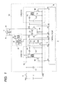
- Fig. 1 is a circuit diagram showing a structure of a lighting device 2 for a vehicle according to a first embodiment.
- the lighting device 2 includes a discharge lamp 4 to be a metal halide lamp, a discharge lamp lighting circuit 100 for driving the discharge lamp 4, an on-vehicle battery (which will be hereinafter referred to as a battery) 6, and a power switch 8.
- the battery 6 generates a DC voltage Vbat of 12 V (or 24 V).
- the power switch 8 is a relay switch provided to control ON/OFF operations of the discharge lamp 4 and is provided in series to the battery 6.
- the discharge lamp lighting circuit 100 raises the smoothed battery voltage Vbat, and carries out an AC conversion, and supplies a voltage thus obtained to the discharge lamp 4. A detailed structure of the discharge lamp lighting circuit 100 is described below.
- the discharge lamp lighting circuit 100 includes a first DC/DC converter CONV1, a second DC/DC converter CONV2, an auxiliary lighting circuit 10, a starter circuit 20, a first switch SW1, a second switch SW2, a current detecting resistor R1, a control circuit 30, and an input capacitor C1.
- the input capacitor C1 is provided in parallel with the battery 6 and smoothes the battery voltage Vbat. More specifically, the input capacitor C1 is provided in the vicinity of a first transformer T1 and a second transformer T2 and fulfills a function of smoothing a voltage with respect to switching operations of the first DC/DC converter CONV1 and the second DC/DC converter CONV2.
- the control circuit 30 is a functional IC (Integrated Circuit) for controlling the whole discharge lamp lighting circuit 100 and serves to control an operation sequence of the discharge lamp lighting circuit 100 and to regulate a power to be supplied to the discharge lamp 4.
- the control circuit 30 executes the following sequences, thereby turning ON the discharge lamp 4 and stabilizing a light output thereof.
- the first DC/DC converter CONV1, the second DC/DC converter CONV2, the first switch SW1, the second switch SW2 and the control circuit 30 form a driving voltage generating portion 12 for generating a driving voltage (which is also referred to as a lamp voltage) VL for the discharge lamp 4.
- the driving voltage generating portion 12 supplies an AC driving voltage VL having a first frequency (a lighting frequency) f1 between both terminals of the discharge lamp 4.
- the first frequency f1 is set to be equal to or lower than 10 kHz, and more specifically, is set to be approximately 250 Hz to 750 Hz.
- the first DC/DC converter CONV1 is an insulating type switching regulator and includes a first switching unit M1, the first transformer T1, a first rectifier diode D1 and a first output capacitor Co1.
- the topology of the first DC/DC converter CONV1 is general, and a brief description is given below.
- a primary coil L1 of the first transformer T1 and the first switching unit M1 are provided in parallel with the input capacitor C1 and in series between an input terminal Pin of the first DC/DC converter CONV1 and a ground terminal (GND).
- the first switching unit M1 is constituted by an N channel MOSFET.
- a secondary coil L2 of the first transformer T1 has one of terminals which is grounded and the other terminal which is connected to an anode of the first rectifier diode D1.
- the first output capacitor Co1 is provided between a cathode of the first rectifier diode D1 and a ground terminal.
- a first control pulse signal S1 having a second frequency f2 which is higher than the first frequency f1 is applied to a control terminal (a gate) of the first switching unit M1.
- the second frequency f2 can be 400 kHz.
- the first switching unit M1 is turned ON when the first control pulse signal S1 has a high level, and is turned OFF when the first control pulse signal S1 has a low level.
- the control circuit 30 regulates a duty ratio of the high level of the first control pulse signal S1 to the low level thereof through a feedback based on an electrical state of the discharge lamp 4.
- the first DC/DC converter CONV1 can be switched into an active state and a non-active state, and supplies a first driving voltage (which will be hereinafter referred to as an output voltage) Vo1 to a terminal P1 of the discharge lamp 4 in the active state.
- a first driving voltage which will be hereinafter referred to as an output voltage
- the second DC/DC converter CONV2 has the same circuit topology as that of the first DC/DC converter CONV1.
- the first rectifier diode D1 and a second rectifier diode D2 the first output capacitor Co1 and a second output capacitor Co2, the first transformer T1 and the second transformer T2, and the first switching unit M1 and a second switching unit M2 correspond to each other.
- ON/OFF operations of the second switching unit M2 are controlled in response to a second control pulse signal S2 generated by the control circuit 30 through a feedback based on the electrical state of the discharge lamp 4.
- the second DC/DC converter CONV2 also can be switched into an active state and a non-active state, and supplies a second driving voltage (which will be hereinafter referred to as a second output voltage) Vo2 to the other terminal P2 of the discharge lamp 4 in the active state.
- a second driving voltage which will be hereinafter referred to as a second output voltage
- the first switch SW1 is provided on the terminal P1 side of the discharge lamp 4 and electrically conducts the terminal P1 of the discharge lamp 4 and a fixed voltage terminal (a ground terminal) in an ON state.
- the second switch SW2 is provided on the other terminal P2 side of the discharge lamp 4 and electrically conducts the other terminal P2 of the discharge lamp 4 and the ground terminal in an ON state.
- IGBT Insulated Gate Bipolar Transistor
- MOSFET Metal Oxide Semiconductor Field Effect Transistor
- the ON/OFF states of the first switch SW1 and the second switch SW2 are controlled in response to control signals S3 and S4 sent from the control circuit 30, respectively.
- the first DC/DC converter CONV1 and the second DC/DC converter CONV2 complementarily repeat the active state and the non-active state in a predetermined cycle T1 (that is, the first frequency f1). In other words, a period for which the first DC/DC converter CONV1 is active and a period for which the second DC/DC converter CONV2 is active have a half of the lighting cycle T1, respectively.
- a state in which the first DC/DC converter CONV1 is active will be hereinafter referred to as a first state ⁇ 1 and a state in which the second DC/DC converter CONV2 is active will be hereinafter referred to as a second state ⁇ 2.
- the first switch SW1 is turned ON when the second DC/DC converter CONV2 is active, that is, in the second state ⁇ 2, and the second switch SW2 is turned ON when the first DC/DC converter CONV1 is active, that is, in the first state ⁇ 1.
- the first driving voltage Vo1 is applied to the terminal P1 of the discharge lamp 4 and a ground voltage (0 V) is applied to the other terminal P2.
- the driving voltage VL (which is almost equal to Vo1) is applied in a first polarity to the discharge lamp 4.
- the second output voltage Vo2 is applied to the other terminal P2 of the discharge lamp 4 and the ground voltage is applied to the terminal P1.
- the driving voltage VL (which is almost equal to Vo2) is applied, to the discharge lamp 4, in a second polarity which is opposite to the first polarity.
- the control circuit 30 alternately repeats the first state ⁇ 1 and the second state ⁇ 2 in the predetermined lighting cycle T1. As a result, the AC driving voltage VL is supplied to the discharge lamp 4.
- the current detecting resistor R1 is provided on a path of a lamp current IL flowing to the discharge lamp 4.
- the current detecting resistor R1 is provided between emitters of the first switch SW1 and the second switch SW2 which are connected in common, and a ground terminal.
- a lamp current having the first polarity in a rightward direction of Fig. 1
- a lamp current having a second polarity in a leftward direction of Fig. 1
- a voltage drop (hereinafter referred to as a current detecting signal S IL ) which is proportional to the lamp current IL is generated in the current detecting resistor R1.
- the current detecting signal S IL is fed back to the control circuit 30.
- the starter circuit 20 is provided for breaking down the discharge lamp 4 and includes a starter transformer 22 and a pulse generating portion 28.
- the pulse generating portion 28 of the starter circuit 20 applies a pulse voltage having an amplitude of 400 V to a primary coil 24 of the starter transformer 22.
- a high voltage pulse for example, 20 kV
- a high voltage pulse for example, 20 kV
- the discharge lamp 4 is broken down so that a discharge is started.
- the auxiliary lighting circuit 10 is provided for causing the discharge lamp 4 to carry out an arc growth.
- the auxiliary lighting circuit 10 includes an auxiliary lighting capacitor C2, an auxiliary lighting resistor R2 and a switch SW3.
- the auxiliary lighting circuit 10 is provided between the terminal P1 of the discharge lamp 4 and the ground terminal, that is, in parallel with the first output capacitor Co1.
- the auxiliary lighting capacitor C2, the auxiliary lighting resistor R2 and the switch SW3 are connected in series.
- the order of the auxiliary lighting capacitor C2, the auxiliary lighting resistor R2 and the switch SW3 is not particularly restricted but may be changed properly.
- the switch SW3 it is possible to utilize various transistor devices such as an MOSFET (Metal Oxide Semiconductor Field Effect Transistor), a bipolar transistor or an IGBT.
- MOSFET Metal Oxide Semiconductor Field Effect Transistor
- the auxiliary lighting capacitor C2 has a capacitance of 1.8 ⁇ F and the auxiliary lighting resistor R2 has a resistance of 180 ⁇ .
- the auxiliary lighting resistor R2 does not need to be provided as a resistance unit but can be replaced with an ON-resistance of the switch SW3 depending on a resistance value thereof. ON/OFF operations of the switch SW3 are controlled in response to a control signal S5 sent from the control circuit 30. A control sequence of the switch SW3 is described below.
- Figs. 2A to 2D are time charts showing an operating state of the discharge lamp lighting circuit 100.
- the ordinate axis and the abscissa axis in each of Figs. 2A to 2D are enlarged or reduced to facilitate understanding, and each waveform illustrated therein is also simplified to facilitate understanding.
- Figs. 2A to 2D show waveforms in a breakdown process, an arc growth process, a run-up process and stationary lighting, respectively.
- the control circuit 30 brings the first DC/DC converter CONV1 and the first switch SW1 into the active state and the OFF state respectively, and raises the battery voltage Vbat into a predetermined high voltage (400 V) to carry out a stabilization. More specifically, the control circuit 30 regulates the duty ratio of the first switching unit M1 by utilizing a PWM (Pulse Width Modulation) or a PFM (Pulse Frequency Modulation) method in such a manner that the output voltage Vo1 of the first DC/DC converter CONV1 is 400 V. For the PWM/PFM control, it is preferable to use a well-known technique.
- PWM Pulse Width Modulation
- PFM Pulse Frequency Modulation
- the PWM control can be implemented by an error amplifier for amplifying an error between the output voltage Vo1 and a reference voltage (Vref) and a comparator for slicing a periodic signal having a triangular wave or a sawtooth wave with an output of the error amplifier and generating the first control pulse signal S1.
- Vref reference voltage
- a comparator for slicing a periodic signal having a triangular wave or a sawtooth wave with an output of the error amplifier and generating the first control pulse signal S1.
- the control method of the first switching unit M1 is not limited to the foregoing techniques.
- the control circuit 30 turns ON the switch SW3.
- the first output capacitor Co1 of the first DC/DC converter CONV1 and the auxiliary lighting capacitor C2 of the auxiliary lighting circuit 10 are charged with the voltage Vo1 (which is almost equal to 400 V) so that energy is stored.
- the starter circuit 20 receives the voltage Vo1 of 400 V generated by the first DC/DC converter CONV1.
- the pulse generating portion 28 applies a pulse having an amplitude of 400 V to the primary coil 24 of the starter transformer 22.
- a high voltage pulse of 20 kV or more is generated in the secondary coil 26 of the starter transformer 22.
- the driving voltage of the discharge lamp 4 is raised to approximately 13 to 15 kV to carry out a breakdown so that a glow discharge is started.
- the control circuit 30 continuously maintains the ON state of the switch SW3.
- a large current of several A (more specifically, approximately 10 A) is supplied from the first output capacitor Co1 and the auxiliary lighting capacitor C2 to the discharge lamp 4.
- the current is supplied from the first output capacitor Co1 to the discharge lamp 4.
- a current delayed corresponding to a time constant formed by the auxiliary lighting resistor R2 and the auxiliary lighting capacitor C2 is supplied from the auxiliary lighting capacitor C2 to the discharge lamp 4.
- Supply of the large current to the discharge lamp 4 is taken over from the first output capacitor Co1 to the auxiliary lighting circuit 10. Therefore, the auxiliary lighting circuit 10 is also referred to as a takeover circuit.
- the control circuit 30 turns OFF the switch SW3 and controls the first DC/DC converter CONV1, the second DC/DC converter CONV2, the first switch SW1 and the second switch SW2, thereby repeating the first state ⁇ 1 and the second state ⁇ 2 complementarily in the predetermined cycle T1.
- the control circuit 30 monitors the first driving voltage Vo1, the second driving voltage Vo2 and the lamp current IL and regulates the duty ratio of the ON/OFF operations of the first switching unit M1 and the second switching unit M2 through a feedback.
- the discharge lamp lighting circuit 100 temporarily supplies a higher overpower than a rated power and then stabilizes the lamp voltage and the lamp current IL into 85 V and 0.4 A to carry out an approximation to the rated power (35 watts (W)).
- the switch SW3 is turned ON before the discharge lamp 4 is turned ON, and is turned OFF after the discharge lamp 4 is turned ON. Description will be given to a switching control of the switch SW3 from ON to OFF which is carried out by the control circuit 30.
- the control of the switch SW3 can be executed in accordance with any of the following methods 1 to 3.
- the control circuit 30 controls the ON/OFF operations of the switch SW3 based on the lamp current IL flowing to the discharge lamp 4. More specifically, the current detecting signal S IL corresponding to the lamp current IL is compared with a threshold signal corresponding to a predetermined threshold current Ith (for example, 0.2 A). When it is estimated that IL ⁇ Ith is set, that is, the discharge lamp 4 is turned OFF, the switch SW3 is turned ON. When it is estimated that IL > Ith is set, that is, the discharge lamp 4 is turned ON, the switch SW3 is turned OFF.
- the control circuit 30 controls the ON/OFF operations of the switch SW3 based on the driving voltage Vo1 (or Vo2) supplied to the discharge lamp 4. More specifically, the driving voltage Vo1 is compared with a predetermined threshold voltage Vth (for example, 250 V). When it is estimated that Vo1 > Vth is set, that is, the discharge lamp 4 is turned OFF, the switch SW3 is turned ON. When it is estimated that Vo1 ⁇ Vth is set, that is, the discharge lamp 4 is turned ON, the switch SW3 is turned OFF.
- the time required from start of the driving operation of the discharge lamp 4 to ON operation of the discharge lamp 4 can be anticipated based on a type of the discharge lamp 4 and characteristics of the first DC/DC converter CONV1, the second DC/DC converter CONV2 and the auxiliary lighting circuit 10. Therefore, the control circuit 30 controls the ON/OFF operations of the switch SW3 based on a timer control. More specifically, a time passing after the start of the driving operation of the discharge lamp 4 (for example, since the ON operation of the power switch 8) is begun to turn ON the switch SW3 before passage of a predetermined amount of time and to turn OFF the switch SW3 after the passage of the predetermined time.
- the power to be supplied to the discharge lamp 4 is stabilized to have a rated value of 35 W so that the light output of the discharge lamp 4 is stabilized ( Fig. 2D ).
- the operation of the discharge lamp lighting circuit 100 according to the embodiment has been described above.
- the discharge lamp lighting circuit 100 can provide the following advantages compared with the conventional discharge lamp lighting circuit.
- the advantage (2) is a peculiar effect to a topology (referred to as a double converter type) in which the two DC/DC converters shown in Fig. 1 are provided on the both terminals of the discharge lamp 4.
- the provision of the switch SW3 is very useful in a discharge lamp lighting circuit of the double converter type.
- FIGs. 3A and 3B are circuit diagrams showing structures of auxiliary lighting circuits 10a and 10b according to the variant.
- the auxiliary lighting circuit 10a in Fig. 3A further includes a diode D3 in addition to the auxiliary lighting circuit 10 in Fig. 1 .
- the diode D3 is disposed in parallel with the switch SW3 in such a direction that an anode is provided on a side of either of the terminal P1 of the discharge lamp 4 and the ground terminal GND which has a lower electric potential.
- the ground terminal GND has a lower electric potential than the terminal P1. Therefore, the anode of the diode D3 is provided on the ground terminal GND side.
- a time of approximately 30 milliseconds (ms) is required from the ON operation of the power switch 8 to the activation of the discharge lamp 4 (a generation of a pulse in the starter circuit 20).
- ms milliseconds
- the charging operation of the auxiliary lighting capacitor C2 should be completed before a breakdown caused by the starter circuit 20.
- a charging current Ic is approximately 0.1 A, therefore, the discharging current to be supplied to the discharge lamp 4 by the auxiliary lighting circuit 10 is large, that is, several A.
- a discharging current Id passes through the switch SW3. For this reason, it is necessary to use a switch corresponding to the discharging current Id, and there is a room for an improvement in respect of a cost or a circuit area.
- the auxiliary lighting circuit 10a in Fig. 3A the charging operation of the auxiliary lighting capacitor C2 is carried out through the switch SW3, and the discharging current Id is mainly supplied from the auxiliary lighting capacitor C2 to the discharge lamp 4 through the diode D3. Accordingly, it is sufficient that the switch SW3 is designed in consideration of a small charging current Ic of approximately 0.1 A. Therefore, it is possible to reduce the size and cost.
- the switch SW3 may be turned OFF for a period of an arc growth.
- the auxiliary lighting circuit 10b in Fig. 3B further includes a discharging current limiting resistor R3 in addition to the structure in Fig. 3A .
- the discharging current limiting resistor R3 is provided in series to the switch SW3 between an anode and a cathode in the diode D3.
- the auxiliary lighting resistor R2 can also be replaced with an ON resistance of a transistor. In place of the bipolar transistor, it is also possible to use an MOSFET or an IGBT.
- the discharging current Id mainly flows to the diode D3 side in the same manner as in Fig. 3A . Therefore, it is possible to use a small bipolar transistor as the switch SW3.
- the discharging current Id tries to flow from an emitter of the bipolar transistor (SW3) to a collector thereof immediately after an activation of the discharge lamp 4. If the current is large, therefore, there is a possibility that the reliability of the switch SW3 will deteriorate.
- a discharging current Ix flowing to the discharge lamp 4 through the switch SW3 can be limited to be equal to or less than (Vf/R3).
- the general discharge lamp lighting circuit 100 has a ground protecting function for deciding whether the both ends P1 and P2 of the discharge lamp 4 are grounded or not and executing a predetermined processing (a shutdown of a circuit or a temporary stoppage of an ON operation) when the grounding is generated.
- a predetermined processing a shutdown of a circuit or a temporary stoppage of an ON operation
- the malfunction is described by taking, as an example, a circuit in which the discharge lamp lighting circuit 100 in Fig. 1 and the lighting auxiliary circuit 10b in Fig. 3B are combined.
- the discharge lamp lighting circuit 100 is turned ON. Subsequently, a transition to a breakdown process and an arc growth process is sequentially carried out. In the arc growth process, an electric charge of the lighting auxiliary capacitor C2 is supplied to the discharge lamp 4.
- the switch SW3 which is turned ON at first is turned OFF with a start of a lighting operation. At this time, an electric charge corresponding to the output voltage Vo1 remains in the lighting auxiliary capacitor C2.
- AC lighting in which the first DC/DC converter CONV1 and the second DC/DC converter CONV2 are alternately made active at a lighting frequency.
- a warm-up is carried out in a certain time before the start of the AC lighting (which is also referred to as a DC period) in some cases.
- the second DC/DC converter CONV2 is fixedly made active and the first switch SW1 is fixedly turned ON so that DC lighting is carried out.
- the control circuit 30 decides, as grounding, a state in which the terminal voltage of the discharge lamp 4 is low and the current does not flow to the discharge lamp 4. More specifically, the decision of the grounding state is made by meeting both of the following two conditions.
- Condition 1 The electric potential of the terminal P1 (P2) of the discharge lamp 4 is lower than a predetermined threshold.
- Condition 2 The voltage drop (S IL ) generated on the current detecting resistor R1 is smaller than a threshold.
- the output of the second DC/DC converter CONV2 (that is, the terminal P2 of the discharge lamp 4) is grounded.
- the condition 1 is met.
- the current flows to the closed loop so that a non-zero voltage drop is generated in the current detecting resistor R1. Therefore, the lighting auxiliary circuit 10 decides that the condition 2 is not met. This implies that the grounding of the second DC/DC converter CONV2 cannot be detected.
- control of the discharge lamp lighting circuit 100 is mismatched, which is not desirable.
- the current detecting resistor R1 is disposed in a place which is not included in a loop formed by the first switch SW1 and the diode D3. In other words, the current detecting resistor R1 is excluded from the loop. In other words, the anode terminal of the diode D3 is connected to a position in which a loop current flowing in the loop including the diode D3 itself and the first switch SW1 does not flow into the current detecting resistor R1.
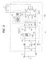
- Fig. 4 is a circuit diagram showing a structure of a discharge lamp lighting circuit 100c according to a first variant.
- a control circuit 30 controls switching of a first DC/DC converter CONV1 and a second DC/DC converter CONV2 based on a voltage drop (a current detecting signal S IL ) generated in a current detecting resistor R1. Furthermore, the control circuit 30 detects grounding of an output of the first DC/DC converter CONV1 based on an electric potential Vo1 of an end P1 of a discharge lamp 4 and the current detecting signal S IL , and detects grounding of an output of the second DC/DC converter CONV2 based on an electric potential Vo2 of the other end P2 of the discharge lamp 4 and the current detecting signal S IL .
- a lighting auxiliary circuit 10c has the same components as those of the lighting auxiliary circuit 10b shown in Fig. 3C , a connecting configuration of a diode D3 is varied. More specifically, the diode D3 has an anode connected to a node on a path connecting a first switch SW1 and the current detecting resistor R1. The other structures are the same.
- control circuit 30 can properly decide the condition 2 for the grounding decision and can detect that the second DC/DC converter CONV2 is set in a grounding state.
- Figs. 5A and 5B are circuit diagrams showing a part of structures of discharge lamp lighting circuits 100d and 100e according to second and third variants.
- the discharge lamp lighting circuit 100d in Fig. 5A is provided with two current detecting resistors R11 and R12.
- the first current detecting resistor R11 is provided between a first switch SW1 and a fixed voltage terminal (a grounding terminal GND), and the second current detecting resistor R12 is provided between a second switch SW2 and the grounding terminal GND.
- a voltage drop generated in the current detecting resistor R11 is fed back, to a control circuit 30 (not shown), as a current detecting signal S IL1 indicative of a current flowing to a discharge lamp 4 in a second state ⁇ 2.
- a voltage drop generated in the current detecting resistor R12 is fed back, to the control circuit 30 (not shown), as a current detecting signal S IL2 indicative of a current flowing to the discharge lamp 4 in a first state ⁇ 1.
- All of the two current detecting resistors R11 and R12 are provided in positions which are not included in a loop formed by a diode D3 and the first switch SW1. More specifically, the diode D3 has a cathode connected to a node on a path connecting the first switch SW1 and the current detecting resistor R11.
- a current detecting resistor R1 is provided between a terminal on a fixing voltage terminal (a grounding terminal) side of a first switch SW1 and a terminal on a grounding terminal side of a second switch SW2. A terminal on the first switch SW1 side in the current detecting resistor R1 is grounded.
- the current detecting resistor R1 is provided in a position which is not included in a loop formed by the diode D3 and the first switch SW1. More specifically, the diode D3 has a cathode connected to a node on a path connecting the first switch SW1 and the current detecting resistor R1.
- a lighting auxiliary circuit 10e in Fig. 5B has a substantially identical structure to that of the lighting auxiliary circuit 10b in Fig. 3B .
- the AC lighting is carried out by using a single DC/DC converter and a switching circuit (an H bridge circuit).
- Fig. 6 is a circuit diagram showing a structure of a lighting device 2a for a vehicle according to the second embodiment. Description of common structures to Fig. 1 will be omitted and only different parts will be explained.
- a discharge lamp lighting circuit 100a includes a DC/DC converter CONV4, an auxiliary lighting circuit 10, a starter circuit 20, an H bridge circuit 40 and an input circuit 42.
- the input circuit 42 includes an input inductor L6, input capacitors C1 and C6, a resistor R6, and an input switch M6.
- the input capacitor C6 is provided in parallel with a battery 6 and smoothes a battery voltage Vbat.
- the input inductor L6 is provided in series to a power switch 8 between the battery 6 and an input terminal Pin of the DC/DC converter CONV4.
- the input capacitor C6 and the input switch M6 are provided in series between the input terminal Pin and a ground terminal GND.
- the resistor R6 is provided between a gate of the input switch M6 and one of terminals of the input capacitor C1.
- the input circuit 42 blocks a leakage of a noise made in the DC/DC converter CONV4 to the battery 6 side.
- the input switch M6 and the resistor R6 are provided for protecting the circuit and have a function for blocking a current when the battery 6 is connected in a reverse polarity.
- the DC/DC converter CONV4 raises the battery voltage Vbat.
- the DC/DC converter CONV4 includes a transformer T4, a rectifier diode D4, an output capacitor Co4 and a switching unit M4.
- One of terminals of a primary coil L4 of the transformer T4 and one of terminals of a secondary coil L5 thereof are connected in common to a drain of the switching unit M4 (MOSFET).
- MOSFET switching unit M4
- a duty ratio of ON/OFF of the switching unit M4 is controlled in the same manner as in the first embodiment.
- An output voltage Vo thus raised is supplied to the H bridge circuit 40 in a subsequent stage.
- the H bridge circuit 40 includes high side switches Q1 and Q3 and low side switches Q2 and Q4 in an IGBT.
- a first state ⁇ 1 in which a pair of the switches Q1 and Q4 is turned ON
- a second state ⁇ 2 in which a pair of the switches Q2 and Q3 is turned ON
- an AC driving voltage is supplied to the discharge lamp 4.
- the DC/DC converter CONV4 and the H bridge circuit 40 function as a driving voltage generating portion 12.
- the auxiliary lighting circuit 10 and the starter circuit 20 are the same as those in the first embodiment.
- the auxiliary lighting circuit 10 has any of structures shown in Figs. 1 , 3A and 3B .
- the discharge lamp lighting circuit 100a in Fig. 6 can provide the following advantages.
- either of the auxiliary lighting circuits 10a and 10b in Figs. 3A and 3B can be provided. It is necessary to dispose the diode D3 in Figs. 3A and 3B in such a direction that either of the terminal P1 of the discharge lamp 4 and the ground terminal GND which has a lower electric potential is set to be the anode. In the case in which the negative electrode lighting is carried out, the terminal P1 side of the discharge lamp 4 has a lower electric potential. Therefore, the diode D3 is to be inverted in such a manner that the anode is set onto the terminal P1 side of the discharge lamp 4.
Landscapes
- Circuit Arrangements For Discharge Lamps (AREA)
Applications Claiming Priority (2)
| Application Number | Priority Date | Filing Date | Title |
|---|---|---|---|
| JP2008279769 | 2008-10-30 | ||
| JP2009021797A JP5460065B2 (ja) | 2008-10-30 | 2009-02-02 | 放電灯点灯回路 |
Publications (2)
| Publication Number | Publication Date |
|---|---|
| EP2197249A1 true EP2197249A1 (fr) | 2010-06-16 |
| EP2197249B1 EP2197249B1 (fr) | 2014-05-07 |
Family
ID=42122754
Family Applications (1)
| Application Number | Title | Priority Date | Filing Date |
|---|---|---|---|
| EP09174402.9A Not-in-force EP2197249B1 (fr) | 2008-10-30 | 2009-10-29 | Circuit d'éclairage de lampe de décharge |
Country Status (4)
| Country | Link |
|---|---|
| US (1) | US8314573B2 (fr) |
| EP (1) | EP2197249B1 (fr) |
| JP (1) | JP5460065B2 (fr) |
| CN (1) | CN101730357B (fr) |
Families Citing this family (2)
| Publication number | Priority date | Publication date | Assignee | Title |
|---|---|---|---|---|
| JP5765121B2 (ja) * | 2011-08-01 | 2015-08-19 | セイコーエプソン株式会社 | 放電灯点灯装置、及び、プロジェクター |
| CN102958222B (zh) * | 2011-08-19 | 2016-09-28 | 国网安徽省电力公司阜阳供电公司 | 供电控制系统 |
Citations (5)
| Publication number | Priority date | Publication date | Assignee | Title |
|---|---|---|---|---|
| GB1496918A (en) * | 1975-08-14 | 1978-01-05 | Cates J | Low pressure discharge lamp starting and operating circui |
| US4134043A (en) * | 1976-04-07 | 1979-01-09 | Esquire, Inc. | Lighting circuits |
| EP0337022A1 (fr) * | 1988-04-12 | 1989-10-18 | Actronic Lighting Cc | Dispositif d'aide au démarrage pour une lampe à décharge |
| US20020047644A1 (en) * | 2000-02-10 | 2002-04-25 | Masayasu Ito | Discharge lamp lighting circuit |
| JP2005322500A (ja) * | 2004-05-10 | 2005-11-17 | Ushio Inc | 高圧放電ランプ点灯装置 |
Family Cites Families (23)
| Publication number | Priority date | Publication date | Assignee | Title |
|---|---|---|---|---|
| GB498107A (en) | 1937-12-30 | 1939-01-03 | Patent Treuhand Ges Fuer Elektrische Gluehlampen Mbh | Improvements in circuit arrangements for operating electric discharge devices |
| US4346332A (en) * | 1980-08-14 | 1982-08-24 | General Electric Company | Frequency shift inverter for variable power control |
| DE3327030A1 (de) * | 1983-07-27 | 1985-02-07 | Philips Patentverwaltung Gmbh, 2000 Hamburg | Schaltungsanordnung zum betrieb von hochdruckgasentladungslampen |
| JP2587718B2 (ja) * | 1990-10-01 | 1997-03-05 | 株式会社小糸製作所 | 車輌用放電灯の点灯回路 |
| SG48126A1 (en) * | 1991-11-13 | 1998-04-17 | Philips Electronics Nv | Circuit arrangement |
| JP3422507B2 (ja) | 1992-01-27 | 2003-06-30 | 三菱電機株式会社 | 放電灯点灯装置 |
| DE4218647A1 (de) * | 1992-01-27 | 1993-08-12 | Mitsubishi Electric Corp | Hochspannungs-entladungslampeneinrichtung |
| JP3125459B2 (ja) * | 1992-08-25 | 2001-01-15 | 三菱電機株式会社 | 放電灯点灯装置 |
| JP3244859B2 (ja) * | 1993-04-12 | 2002-01-07 | 池田デンソー株式会社 | 放電灯点灯装置 |
| US5410221A (en) * | 1993-04-23 | 1995-04-25 | Philips Electronics North America Corporation | Lamp ballast with frequency modulated lamp frequency |
| DE19544842A1 (de) * | 1995-12-01 | 1997-06-05 | Bosch Gmbh Robert | Eingangsbeschaltung für eine Zündvorrichtung einer Hochdruck-Gasentladungslampe |
| JP3384323B2 (ja) | 1998-05-08 | 2003-03-10 | 株式会社デンソー | 放電灯装置 |
| US7327095B2 (en) * | 2000-05-24 | 2008-02-05 | Mitsubishi Denki Kabushiki Kaisha | Discharge lamp lighting apparatus |
| JP2002015889A (ja) * | 2000-06-30 | 2002-01-18 | Matsushita Electric Works Ltd | 高圧放電灯点灯装置 |
| AU2002349518A1 (en) * | 2001-11-27 | 2003-06-10 | Matsushita Electric Works, Ltd. | Electronic ballast for high-pressure discharge lamp |
| ATE401763T1 (de) * | 2002-01-08 | 2008-08-15 | Koninkl Philips Electronics Nv | Schaltung für eine gasentladungslampe |
| EP1558064B1 (fr) * | 2002-10-28 | 2014-07-09 | Panasonic Corporation | Dispositif d'actionnement d'une lampe a decharge haute pression et appareil d'eclairage comprenant ce dispositif |
| JP2004296119A (ja) * | 2003-03-25 | 2004-10-21 | Tdk Corp | 放電灯点灯装置 |
| US7622869B2 (en) * | 2004-02-24 | 2009-11-24 | Panasonic Electric Works Co., Ltd. | Discharge lamp ballast and projector |
| DE102005023171A1 (de) * | 2004-05-28 | 2005-12-22 | Harison Toshiba Lighting Corp. | Lichtvorrichtung für Entladungslampen |
| JP2006260808A (ja) * | 2005-03-15 | 2006-09-28 | Sanyo Tekunika:Kk | 高輝度放電バルブの制御装置とその制御方法 |
| JP2006344495A (ja) * | 2005-06-09 | 2006-12-21 | Ushio Inc | 放電ランプ点灯装置 |
| JP5349920B2 (ja) * | 2008-03-05 | 2013-11-20 | 株式会社小糸製作所 | 放電灯点灯回路 |
-
2009
- 2009-02-02 JP JP2009021797A patent/JP5460065B2/ja not_active Expired - Fee Related
- 2009-10-29 US US12/608,089 patent/US8314573B2/en not_active Expired - Fee Related
- 2009-10-29 EP EP09174402.9A patent/EP2197249B1/fr not_active Not-in-force
- 2009-10-30 CN CN200910205595.3A patent/CN101730357B/zh not_active Expired - Fee Related
Patent Citations (5)
| Publication number | Priority date | Publication date | Assignee | Title |
|---|---|---|---|---|
| GB1496918A (en) * | 1975-08-14 | 1978-01-05 | Cates J | Low pressure discharge lamp starting and operating circui |
| US4134043A (en) * | 1976-04-07 | 1979-01-09 | Esquire, Inc. | Lighting circuits |
| EP0337022A1 (fr) * | 1988-04-12 | 1989-10-18 | Actronic Lighting Cc | Dispositif d'aide au démarrage pour une lampe à décharge |
| US20020047644A1 (en) * | 2000-02-10 | 2002-04-25 | Masayasu Ito | Discharge lamp lighting circuit |
| JP2005322500A (ja) * | 2004-05-10 | 2005-11-17 | Ushio Inc | 高圧放電ランプ点灯装置 |
Also Published As
| Publication number | Publication date |
|---|---|
| JP2010135276A (ja) | 2010-06-17 |
| JP5460065B2 (ja) | 2014-04-02 |
| US20100109573A1 (en) | 2010-05-06 |
| EP2197249B1 (fr) | 2014-05-07 |
| US8314573B2 (en) | 2012-11-20 |
| CN101730357B (zh) | 2014-02-26 |
| CN101730357A (zh) | 2010-06-09 |
Similar Documents
| Publication | Publication Date | Title |
|---|---|---|
| US11342836B2 (en) | Overvoltage protection for active clamp flyback converter | |
| US20080043506A1 (en) | Dc-ac converter | |
| JP4632023B2 (ja) | 電力変換装置 | |
| US8174202B2 (en) | Lamp driving circuit | |
| US8710769B2 (en) | Discharge lamp lighting circuit | |
| JP2001006890A (ja) | 放電灯点灯回路 | |
| US8120264B2 (en) | Discharge lamp lighting circuit | |
| JP2010198860A (ja) | 放電灯点灯回路 | |
| EP2197249B1 (fr) | Circuit d'éclairage de lampe de décharge | |
| US7184279B2 (en) | Solid state switching circuit | |
| JP3820931B2 (ja) | 放電灯点灯装置 | |
| US20060214606A1 (en) | Discharge tube operation device | |
| US7545133B2 (en) | Power supply apparatus | |
| JP4984062B2 (ja) | 放電灯点灯装置 | |
| KR20210129894A (ko) | 직류-직류 컨버터 및 그 제어 방법 | |
| WO2021005894A1 (fr) | Convertisseur cc-cc et dispositif d'alimentation électrique | |
| JP3671243B2 (ja) | 共振型電力変換装置 | |
| JP2010140825A (ja) | 放電灯点灯回路 | |
| JP2002051548A (ja) | 電源装置および放電灯点灯装置 | |
| JP6417844B2 (ja) | 放電灯点灯装置 | |
| KR20170006475A (ko) | SMPS (Switching Mode Power Supply) 기반의 LED 구동장치 및 구동방법 | |
| CN101167409A (zh) | 放电灯点灯装置 | |
| JP2025119119A (ja) | スイッチング電源装置 | |
| JP3692095B2 (ja) | スイッチング電源 | |
| JP3928256B2 (ja) | 放電灯点灯装置 |
Legal Events
| Date | Code | Title | Description |
|---|---|---|---|
| PUAI | Public reference made under article 153(3) epc to a published international application that has entered the european phase |
Free format text: ORIGINAL CODE: 0009012 |
|
| 17P | Request for examination filed |
Effective date: 20091029 |
|
| AK | Designated contracting states |
Kind code of ref document: A1 Designated state(s): AT BE BG CH CY CZ DE DK EE ES FI FR GB GR HR HU IE IS IT LI LT LU LV MC MK MT NL NO PL PT RO SE SI SK SM TR |
|
| AX | Request for extension of the european patent |
Extension state: AL BA RS |
|
| 17Q | First examination report despatched |
Effective date: 20120127 |
|
| GRAP | Despatch of communication of intention to grant a patent |
Free format text: ORIGINAL CODE: EPIDOSNIGR1 |
|
| INTG | Intention to grant announced |
Effective date: 20131125 |
|
| GRAS | Grant fee paid |
Free format text: ORIGINAL CODE: EPIDOSNIGR3 |
|
| GRAA | (expected) grant |
Free format text: ORIGINAL CODE: 0009210 |
|
| AK | Designated contracting states |
Kind code of ref document: B1 Designated state(s): AT BE BG CH CY CZ DE DK EE ES FI FR GB GR HR HU IE IS IT LI LT LU LV MC MK MT NL NO PL PT RO SE SI SK SM TR |
|
| REG | Reference to a national code |
Ref country code: GB Ref legal event code: FG4D |
|
| REG | Reference to a national code |
Ref country code: AT Ref legal event code: REF Ref document number: 667507 Country of ref document: AT Kind code of ref document: T Effective date: 20140515 |
|
| REG | Reference to a national code |
Ref country code: IE Ref legal event code: FG4D |
|
| REG | Reference to a national code |
Ref country code: DE Ref legal event code: R096 Ref document number: 602009023824 Country of ref document: DE Effective date: 20140618 |
|
| REG | Reference to a national code |
Ref country code: AT Ref legal event code: MK05 Ref document number: 667507 Country of ref document: AT Kind code of ref document: T Effective date: 20140507 |
|
| REG | Reference to a national code |
Ref country code: NL Ref legal event code: VDEP Effective date: 20140507 |
|
| REG | Reference to a national code |
Ref country code: LT Ref legal event code: MG4D |
|
| PG25 | Lapsed in a contracting state [announced via postgrant information from national office to epo] |
Ref country code: LT Free format text: LAPSE BECAUSE OF FAILURE TO SUBMIT A TRANSLATION OF THE DESCRIPTION OR TO PAY THE FEE WITHIN THE PRESCRIBED TIME-LIMIT Effective date: 20140507 Ref country code: NO Free format text: LAPSE BECAUSE OF FAILURE TO SUBMIT A TRANSLATION OF THE DESCRIPTION OR TO PAY THE FEE WITHIN THE PRESCRIBED TIME-LIMIT Effective date: 20140807 Ref country code: GR Free format text: LAPSE BECAUSE OF FAILURE TO SUBMIT A TRANSLATION OF THE DESCRIPTION OR TO PAY THE FEE WITHIN THE PRESCRIBED TIME-LIMIT Effective date: 20140808 Ref country code: IS Free format text: LAPSE BECAUSE OF FAILURE TO SUBMIT A TRANSLATION OF THE DESCRIPTION OR TO PAY THE FEE WITHIN THE PRESCRIBED TIME-LIMIT Effective date: 20140907 Ref country code: FI Free format text: LAPSE BECAUSE OF FAILURE TO SUBMIT A TRANSLATION OF THE DESCRIPTION OR TO PAY THE FEE WITHIN THE PRESCRIBED TIME-LIMIT Effective date: 20140507 Ref country code: CY Free format text: LAPSE BECAUSE OF FAILURE TO SUBMIT A TRANSLATION OF THE DESCRIPTION OR TO PAY THE FEE WITHIN THE PRESCRIBED TIME-LIMIT Effective date: 20140507 |
|
| PG25 | Lapsed in a contracting state [announced via postgrant information from national office to epo] |
Ref country code: SE Free format text: LAPSE BECAUSE OF FAILURE TO SUBMIT A TRANSLATION OF THE DESCRIPTION OR TO PAY THE FEE WITHIN THE PRESCRIBED TIME-LIMIT Effective date: 20140507 Ref country code: HR Free format text: LAPSE BECAUSE OF FAILURE TO SUBMIT A TRANSLATION OF THE DESCRIPTION OR TO PAY THE FEE WITHIN THE PRESCRIBED TIME-LIMIT Effective date: 20140507 Ref country code: LV Free format text: LAPSE BECAUSE OF FAILURE TO SUBMIT A TRANSLATION OF THE DESCRIPTION OR TO PAY THE FEE WITHIN THE PRESCRIBED TIME-LIMIT Effective date: 20140507 Ref country code: AT Free format text: LAPSE BECAUSE OF FAILURE TO SUBMIT A TRANSLATION OF THE DESCRIPTION OR TO PAY THE FEE WITHIN THE PRESCRIBED TIME-LIMIT Effective date: 20140507 Ref country code: PL Free format text: LAPSE BECAUSE OF FAILURE TO SUBMIT A TRANSLATION OF THE DESCRIPTION OR TO PAY THE FEE WITHIN THE PRESCRIBED TIME-LIMIT Effective date: 20140507 Ref country code: ES Free format text: LAPSE BECAUSE OF FAILURE TO SUBMIT A TRANSLATION OF THE DESCRIPTION OR TO PAY THE FEE WITHIN THE PRESCRIBED TIME-LIMIT Effective date: 20140507 |
|
| PG25 | Lapsed in a contracting state [announced via postgrant information from national office to epo] |
Ref country code: PT Free format text: LAPSE BECAUSE OF FAILURE TO SUBMIT A TRANSLATION OF THE DESCRIPTION OR TO PAY THE FEE WITHIN THE PRESCRIBED TIME-LIMIT Effective date: 20140908 |
|
| PG25 | Lapsed in a contracting state [announced via postgrant information from national office to epo] |
Ref country code: RO Free format text: LAPSE BECAUSE OF FAILURE TO SUBMIT A TRANSLATION OF THE DESCRIPTION OR TO PAY THE FEE WITHIN THE PRESCRIBED TIME-LIMIT Effective date: 20140507 Ref country code: BE Free format text: LAPSE BECAUSE OF FAILURE TO SUBMIT A TRANSLATION OF THE DESCRIPTION OR TO PAY THE FEE WITHIN THE PRESCRIBED TIME-LIMIT Effective date: 20140507 Ref country code: CZ Free format text: LAPSE BECAUSE OF FAILURE TO SUBMIT A TRANSLATION OF THE DESCRIPTION OR TO PAY THE FEE WITHIN THE PRESCRIBED TIME-LIMIT Effective date: 20140507 Ref country code: SK Free format text: LAPSE BECAUSE OF FAILURE TO SUBMIT A TRANSLATION OF THE DESCRIPTION OR TO PAY THE FEE WITHIN THE PRESCRIBED TIME-LIMIT Effective date: 20140507 Ref country code: DK Free format text: LAPSE BECAUSE OF FAILURE TO SUBMIT A TRANSLATION OF THE DESCRIPTION OR TO PAY THE FEE WITHIN THE PRESCRIBED TIME-LIMIT Effective date: 20140507 Ref country code: EE Free format text: LAPSE BECAUSE OF FAILURE TO SUBMIT A TRANSLATION OF THE DESCRIPTION OR TO PAY THE FEE WITHIN THE PRESCRIBED TIME-LIMIT Effective date: 20140507 |
|
| REG | Reference to a national code |
Ref country code: DE Ref legal event code: R097 Ref document number: 602009023824 Country of ref document: DE |
|
| PG25 | Lapsed in a contracting state [announced via postgrant information from national office to epo] |
Ref country code: NL Free format text: LAPSE BECAUSE OF FAILURE TO SUBMIT A TRANSLATION OF THE DESCRIPTION OR TO PAY THE FEE WITHIN THE PRESCRIBED TIME-LIMIT Effective date: 20140507 |
|
| PLBE | No opposition filed within time limit |
Free format text: ORIGINAL CODE: 0009261 |
|
| STAA | Information on the status of an ep patent application or granted ep patent |
Free format text: STATUS: NO OPPOSITION FILED WITHIN TIME LIMIT |
|
| 26N | No opposition filed |
Effective date: 20150210 |
|
| PG25 | Lapsed in a contracting state [announced via postgrant information from national office to epo] |
Ref country code: IT Free format text: LAPSE BECAUSE OF FAILURE TO SUBMIT A TRANSLATION OF THE DESCRIPTION OR TO PAY THE FEE WITHIN THE PRESCRIBED TIME-LIMIT Effective date: 20140507 |
|
| REG | Reference to a national code |
Ref country code: DE Ref legal event code: R097 Ref document number: 602009023824 Country of ref document: DE Effective date: 20150210 |
|
| PG25 | Lapsed in a contracting state [announced via postgrant information from national office to epo] |
Ref country code: LU Free format text: LAPSE BECAUSE OF FAILURE TO SUBMIT A TRANSLATION OF THE DESCRIPTION OR TO PAY THE FEE WITHIN THE PRESCRIBED TIME-LIMIT Effective date: 20141029 Ref country code: MC Free format text: LAPSE BECAUSE OF FAILURE TO SUBMIT A TRANSLATION OF THE DESCRIPTION OR TO PAY THE FEE WITHIN THE PRESCRIBED TIME-LIMIT Effective date: 20140507 |
|
| REG | Reference to a national code |
Ref country code: CH Ref legal event code: PL |
|
| REG | Reference to a national code |
Ref country code: IE Ref legal event code: MM4A |
|
| PG25 | Lapsed in a contracting state [announced via postgrant information from national office to epo] |
Ref country code: CH Free format text: LAPSE BECAUSE OF NON-PAYMENT OF DUE FEES Effective date: 20141031 Ref country code: SI Free format text: LAPSE BECAUSE OF FAILURE TO SUBMIT A TRANSLATION OF THE DESCRIPTION OR TO PAY THE FEE WITHIN THE PRESCRIBED TIME-LIMIT Effective date: 20140507 Ref country code: LI Free format text: LAPSE BECAUSE OF NON-PAYMENT OF DUE FEES Effective date: 20141031 |
|
| PG25 | Lapsed in a contracting state [announced via postgrant information from national office to epo] |
Ref country code: IE Free format text: LAPSE BECAUSE OF NON-PAYMENT OF DUE FEES Effective date: 20141029 |
|
| PGFP | Annual fee paid to national office [announced via postgrant information from national office to epo] |
Ref country code: GB Payment date: 20151028 Year of fee payment: 7 |
|
| PG25 | Lapsed in a contracting state [announced via postgrant information from national office to epo] |
Ref country code: SM Free format text: LAPSE BECAUSE OF FAILURE TO SUBMIT A TRANSLATION OF THE DESCRIPTION OR TO PAY THE FEE WITHIN THE PRESCRIBED TIME-LIMIT Effective date: 20140507 |
|
| PG25 | Lapsed in a contracting state [announced via postgrant information from national office to epo] |
Ref country code: BG Free format text: LAPSE BECAUSE OF FAILURE TO SUBMIT A TRANSLATION OF THE DESCRIPTION OR TO PAY THE FEE WITHIN THE PRESCRIBED TIME-LIMIT Effective date: 20140507 |
|
| PG25 | Lapsed in a contracting state [announced via postgrant information from national office to epo] |
Ref country code: HU Free format text: LAPSE BECAUSE OF FAILURE TO SUBMIT A TRANSLATION OF THE DESCRIPTION OR TO PAY THE FEE WITHIN THE PRESCRIBED TIME-LIMIT; INVALID AB INITIO Effective date: 20091029 Ref country code: MT Free format text: LAPSE BECAUSE OF FAILURE TO SUBMIT A TRANSLATION OF THE DESCRIPTION OR TO PAY THE FEE WITHIN THE PRESCRIBED TIME-LIMIT Effective date: 20140507 Ref country code: TR Free format text: LAPSE BECAUSE OF FAILURE TO SUBMIT A TRANSLATION OF THE DESCRIPTION OR TO PAY THE FEE WITHIN THE PRESCRIBED TIME-LIMIT Effective date: 20140507 |
|
| REG | Reference to a national code |
Ref country code: FR Ref legal event code: PLFP Year of fee payment: 8 |
|
| GBPC | Gb: european patent ceased through non-payment of renewal fee |
Effective date: 20161029 |
|
| PG25 | Lapsed in a contracting state [announced via postgrant information from national office to epo] |
Ref country code: GB Free format text: LAPSE BECAUSE OF NON-PAYMENT OF DUE FEES Effective date: 20161029 |
|
| REG | Reference to a national code |
Ref country code: FR Ref legal event code: PLFP Year of fee payment: 9 |
|
| PGFP | Annual fee paid to national office [announced via postgrant information from national office to epo] |
Ref country code: FR Payment date: 20170918 Year of fee payment: 9 |
|
| PGFP | Annual fee paid to national office [announced via postgrant information from national office to epo] |
Ref country code: DE Payment date: 20171025 Year of fee payment: 9 |
|
| PG25 | Lapsed in a contracting state [announced via postgrant information from national office to epo] |
Ref country code: MK Free format text: LAPSE BECAUSE OF FAILURE TO SUBMIT A TRANSLATION OF THE DESCRIPTION OR TO PAY THE FEE WITHIN THE PRESCRIBED TIME-LIMIT Effective date: 20140507 |
|
| REG | Reference to a national code |
Ref country code: DE Ref legal event code: R119 Ref document number: 602009023824 Country of ref document: DE |
|
| PG25 | Lapsed in a contracting state [announced via postgrant information from national office to epo] |
Ref country code: DE Free format text: LAPSE BECAUSE OF NON-PAYMENT OF DUE FEES Effective date: 20190501 |
|
| PG25 | Lapsed in a contracting state [announced via postgrant information from national office to epo] |
Ref country code: FR Free format text: LAPSE BECAUSE OF NON-PAYMENT OF DUE FEES Effective date: 20181031 |