EP2197657B1 - Verfahren zur herstellung einer linsenanordnung sowie mit einer derartigen anordnung ausgestattete kamera - Google Patents
Verfahren zur herstellung einer linsenanordnung sowie mit einer derartigen anordnung ausgestattete kamera Download PDFInfo
- Publication number
- EP2197657B1 EP2197657B1 EP08838322.9A EP08838322A EP2197657B1 EP 2197657 B1 EP2197657 B1 EP 2197657B1 EP 08838322 A EP08838322 A EP 08838322A EP 2197657 B1 EP2197657 B1 EP 2197657B1
- Authority
- EP
- European Patent Office
- Prior art keywords
- lens element
- lens
- film
- assembly
- spacer
- Prior art date
- Legal status (The legal status is an assumption and is not a legal conclusion. Google has not performed a legal analysis and makes no representation as to the accuracy of the status listed.)
- Active
Links
Images





Classifications
-
- B—PERFORMING OPERATIONS; TRANSPORTING
- B29—WORKING OF PLASTICS; WORKING OF SUBSTANCES IN A PLASTIC STATE IN GENERAL
- B29D—PRODUCING PARTICULAR ARTICLES FROM PLASTICS OR FROM SUBSTANCES IN A PLASTIC STATE
- B29D11/00—Producing optical elements, e.g. lenses or prisms
- B29D11/00009—Production of simple or compound lenses
- B29D11/00278—Lenticular sheets
-
- B—PERFORMING OPERATIONS; TRANSPORTING
- B29—WORKING OF PLASTICS; WORKING OF SUBSTANCES IN A PLASTIC STATE IN GENERAL
- B29D—PRODUCING PARTICULAR ARTICLES FROM PLASTICS OR FROM SUBSTANCES IN A PLASTIC STATE
- B29D11/00—Producing optical elements, e.g. lenses or prisms
- B29D11/00009—Production of simple or compound lenses
- B29D11/00365—Production of microlenses
- B29D11/00375—Production of microlenses by moulding lenses in holes through a substrate
-
- B—PERFORMING OPERATIONS; TRANSPORTING
- B29—WORKING OF PLASTICS; WORKING OF SUBSTANCES IN A PLASTIC STATE IN GENERAL
- B29D—PRODUCING PARTICULAR ARTICLES FROM PLASTICS OR FROM SUBSTANCES IN A PLASTIC STATE
- B29D11/00—Producing optical elements, e.g. lenses or prisms
- B29D11/0073—Optical laminates
-
- G—PHYSICS
- G02—OPTICS
- G02B—OPTICAL ELEMENTS, SYSTEMS OR APPARATUS
- G02B7/00—Mountings, adjusting means, or light-tight connections, for optical elements
- G02B7/02—Mountings, adjusting means, or light-tight connections, for optical elements for lenses
-
- H—ELECTRICITY
- H04—ELECTRIC COMMUNICATION TECHNIQUE
- H04N—PICTORIAL COMMUNICATION, e.g. TELEVISION
- H04N23/00—Cameras or camera modules comprising electronic image sensors; Control thereof
- H04N23/57—Mechanical or electrical details of cameras or camera modules specially adapted for being embedded in other devices
Definitions
- the present invention relates to a method of manufacturing a lens assembly by means of a replication process.
- the invention further relates to a lens assembly, a lens stack as well as a camera provided with such a lens assembly.
- the replication process referred to in the introduction is known per se from U.S. Pat. Nos. 4,756,972 and 4,890,905 , which disclose the possibility of manufacturing a high-quality optical component by means of a replication process.
- Such a replication process is considered to be a quick and inexpensive manner of manufacturing optical components in large numbers.
- a mould having a precisely defined surface for example an aspherical surface, is used, and a small amount of a radiation curable resin, for example a UV curable resin, is applied to the mould surface.
- the resin is spread over the mould surface, so that the cavities in the mould are filled with the resin, after which the whole is irradiated so as to cure the resin and the thus cured product is removed from the mould.
- the cured product is a negative of the mould surface.
- EP 1 180 428 relates to a method for manufacturing a plastic optical device on a substrate comprising the steps of providing a mold with mold cavities, filling a shaping material in the mold cavities of the mold, joining the shaping material with the substrate; hardening the shaping material; and removing the mold to obtain the plastic optical device.
- the substrate is made of a material such as acrylic, glass, or resin.
- the object of the present invention is to provide a method of manufacturing a lens assembly by means of a replication process in which the glass substrate that is usually used is no longer required.
- Another object of the present invention is to provide a method of manufacturing a lens assembly by means of a replication process which minimises the occurrence of shrink phenomena during the curing of the resin.
- Another object of the present invention is to provide a method of manufacturing a lens assembly by means of a replication process in which a high positional accuracy of the lenses relative to each other is achieved.
- Another object of the present invention is to provide a method of manufacturing a lens assembly by means of a replication process in which a substantially monolithic structure of optical elements is achieved, wherein various optical functions can be combined.
- Yet another object of the present invention is to provide a method of manufacturing a lens assembly by means of a replication process by which lenses having a minimum thickness can be produced.
- Both lens elements are thus obtained by using a replication process.
- the first composition is different from the second composition it is possible to impart specific optical properties to the thus manufactured lens assembly, which can also be realised by using a different shape for the cavities of the first mould than for the recesses of the second mould.
- step vii) comprising the placement of a spacer plate on the second composition cured in step v) so as to obtain a first assembly comprising a spacer plate, a second lens element and a first lens element.
- a spacer plate comprises an opening which is positioned coaxially with a main optical axis of the lens element in question, whilst in a special embodiment the side of said opening is provided with an anti-reflective coating.
- a film is arranged over the uncured first composition prior to carrying out step ii), which film seals the first composition yet to be cured which is present in the cavities of the first mould.
- specific optical properties can be obtained, in particular such as diaphragm, anti-reflection, infrared reflection and aperture, but also electric conductivity.
- electrically conductive film it has been found to be possible to influence the refractive index of the lenses replicated on the film. Another possibility would be to supply a current to the electrically conductive film, thus making it possible to adapt the curvature of the lenses replicated on the film.
- the film has the special property that the occurrence of shrink phenomena during the curing of the resin can be minimised, so that lense irregularities are prevented.
- the film is a flexible film having a thickness of maximally 0.75 mm, in particular maximally 0.5 mm, more in particular maximally 0.2 mm, which film does not become detached from the contours formed by the cured polymeric material present in the mould during the curing process.
- a film which is suitable for that purpose is transparent to the wavelength that is used, generally in the visible range, viz. 400-700 nm, but also in the infrared range.
- no air inclusions may be present between the composition to be cured and the film covering said composition.
- optical polymers of the acrylate, epoxy and similar types can be mentioned as materials for the film.
- suitable film materials are polycarbonate film having a thickness of 0.2 mm, glass type D263T (marketed by Schott) having a thickness of 0.2 mm, Melinex (trademark) PET (marketed by DuPont).
- Other materials for the film are polyvinyl butyral, polyester, polyurethane or PVC. Specific components may be added to the aforesaid film for the purpose of influencing the optical and mechanical properties, in which connection pigments, fillers and anti-shrinkage agents may be considered.
- the film functions to influence the optical properties. No bearing properties can be attributed to the film.
- step vi) it has also been found to be possible to place the first assembly on the product obtained after step vi), in which the second mould is removed, so as to obtain a second assembly consisting of, successively, a first lens element, a second lens element, a spacer plate, a second lens element and a first lens element.
- the present invention thus relates to a lens assembly according to claim 5. It is also possible to arrange a third or fourth lens element on top of the spacer, on the side remote from the first lens element, in which case the above-described replication process may be used.
- the present invention further relates to a lens stack as defined in claim 10 as well as to a camera or light source according to claim 14 in which such a stack is used.
- Suitable UV curable compositions include GAFGARD233 (marketed by DuPont, type vinylpyrrolidone), Norland Inc. NOA-61, NOA-63, NOA-65, Three bond AVR-100 and Sony Chemical UV-1003, possibly provided with the usual additives such as initiators, reactive or nonreactive dilutants, crosslinking agents, fillers, pigments and anti-shrinkage agents.
- the present lens assembly is in particular used in cameras, in which small-size lenses are required.
- large-scale production of such lenses must be possible, whilst the positional accuracy of the lenses relative to each other, in combination with the spacer plate, is highly critical.
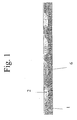
- Figure 1 schematically shows a first mould 1, which is provided with regularly spaced-apart cavities 6, which cavities 6 have been filled with a first, liquid, UV curable composition 2.
- a film 3 is applied, as is shown in figure 2a .
- a silane-type adhesion promoter it is preferable to use.
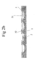
- Figure 2b schematically shows another embodiment of the film 3, which film 3 is provided with transparent parts 51, alternated with non-transparent parts 52, and which is positioned on the first composition 2 in such a manner that the transparent parts 51 more or less coincide with the light path that will pass through the composition 2 formed as a lens.
- the use of non-transparent parts 52 prevents the incident light on one lens part moving to the adjacent lens part, which phenomenon is also known as "crosstalk".
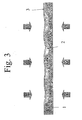
- UV irradiation takes place, with figure 3 clearly showing that the flexible film 3 present on the first composition 2 will follow the shrinkage caused by the UV curing of said first composition 2.
- a second, liquid, UV curable composition 5 is applied to the film 3, as shown in figure 4 , whereupon a second mould 4 provided with recesses 7 is placed on the still liquid second composition 5, in such a manner that the second, liquid composition 5 will spread over the surface of the film 3 and the recesses 7 and the parts present between the recesses 7 on the second mould 4 will be provided with the second composition 5.
- the second mould 4 which is provided with recesses 7, is so positioned relative to the first mould 1 that the cavities 6 of the first mould 1 will be located opposite the recesses 7 of the second mould 4. Subsequently, UV curing will take place again, possibly followed by post-curing, after which the second mould 4 will be removed, as is shown in figure 5a , with a first lens element 2 comprising cured lenses arranged beside each other thus being present in the first mould 1, which first lens element 2 is provided with a film 3, on which a second lens element 5 obtained from the second mould 4 is present.
- the lenses both of the first lens element 2 and of the second lens element 4 are cured compositions. Because use is made of a first mould 1 and a second mould 4, the surfaces both of the first lens element 2 and of the second lens element 4 will be the negative of the surfaces of the moulds 1, 2 in question, which can be called typical of the present replication process.
- Figure 5b shows an embodiment in which the second mould 4 has a convex surface 50, so that the second, liquid composition 5 will exhibit a concave configuration, in contrast to the convex configuration shown in figure 5a , so that the second mould 4 will be pressed against the first mould 1.
- Figure 5b furthermore schematically shows a film 3, from which it appears that the transparent parts 51 are located in the light path that passes through the first composition 2 and the second composition 5.
- a second mould 4 (not shown) which comprises a convex surface as well as a surface provided with recesses.
- the non-transparent parts 52 are so positioned in the two lens elements 2, 5 that the crosstalk phenomenon cannot occur.
- Suitable UV curable compositions are: polycarbonates, including diethylene glycolbis-(allyl)carbonate, polystyrenes, including polychlorine styrene, polyacrylates, such as poly(trifluoroethyl methacrylate), poly(isobutyl methacrylate), poly(methylacrylate), poly(methyl methacrylate), poly(alphamethyl bromium acrylate), poly(methacrylic acid)-2,3-dibromium propylpoly(phenyl methacrylate poly(pentachlorine phenyl-methacrylate polymer), polyester compounds such as diallylphthalate, poly(vinyl-benzoate), poly(vinylnaphthalene), poly(vinylcarbazole) and silicones in the form of various types of resin materials, as well as acrylic resin, urethane resin, epoxy resin, enthiol resin or thiourethane resin or photopolymer.
- polyacrylates such as poly(triflu
- Exposure preferably takes place with an intensity of between 100 en 2000 W/cm 2 , in particular 700 W/cm 2 , and a dose of 1 - 15 J/cm 2 , in particular 7 J/cm 2 , a wavelength in the 320-400 nm range and an exposure time of 1-60 seconds, in particular 10 seconds.
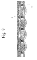
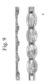
- a spacer plate 8 as shown in figure 6 is placed on the second lens element, in particular on the cured composition 5 present between the lenses of the second lens element, which spacer plate has a thickness or height such that the convexity of the second lens element is less than the aforesaid height or thickness, after which the first mould 1 is removed, as shown in figure 7 , thus obtaining an assembly consisting of, successively, the spacer plate, the second lens element, the film, and the first lens element.
- the spacer plate 8 is bonded to the second lens element via a UV curable or thermosetting adhesive (not shown).
- the spacer plate 8 is made of a rigid material, for example glass, silicon or a composite material such as FR4.
- the spacer plate 8 is so configured that it will not interfere with the light path through the two separate lens elements, and possibly the film 3 present therebetween.
- the spacer plate comprises an opening which is positioned coaxially with a main optical axis of the lens element in question, whilst in a special embodiment the side of said opening is provided with an anti-reflective coating.
- the spacer plate 8 is thus only in contact with the second lens element at the position where the composition 5 has cured on the parts of the mould 4 present between the recesses 7 (see figures 5a/5b ).
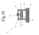
- FIG 10 schematically shows a lens stack 20 in which a lens assembly obtained by using the present method is used.
- An optically active element for example a VCSL (light source), a CCD / CMOS sensor 21, is provided with a spacer 22, whilst a glass plate 23 extending along the length of the optical element 21 is positioned on the spacer 22, which glass plate 23 is provided on either side thereof with lenses 28, 29 replicated thereon.
- a spacer 24 is disposed, on which spacer 24 a lens element manufactured according to the present method is present, which comprises a film 25 that is provided with replicated lens elements 26, 27 on either side thereof.
- the spacers 22, 24, the glass plate 23 and the lens elements 28, 29, 27, 26 are bonded together by means of adhesives, for which thicknesses in the order of 5-100 ⁇ m may be used.
- the aforesaid spacers are made of glass, and the replicated lens elements are polymer-based. Although it is indicated herein that the film 25 and the two lens elements 26, 27 replicated thereon are located furthest away from the optically active element 21, it is also possible to use embodiments in which the aforesaid film 25 and the lens elements 26, 27 are located closest to the optically active element 21.
- the spacer 22 may be made of the same material as the previously discussed spacer 8.
- the spacer 22 comprises an opening which is positioned coaxially with a main optical axis of the lens element in question, whilst in a special embodiment the side of said opening is provided with an anti-reflective coating.
- FIG 11 schematically shows a lens stack 30, in which an optically active element, such as a VCSL (light source), a megapixel CMOS sensor 31, is provided with a spacer 32, on which spacer 32 a glass plate 33 is positioned, which glass plate 33 is provided on either side thereof with lens elements 43, 42 replicated thereon.
- the spacer 34 is integrated in the lens element 43, which means that the lens element 43 and the spacer 34 form a uniform or inseparable whole.
- the spacer 34 is provided as a separate component, with the lens elements 40, the spacer 34 and the lens element 43 thus being durably interconnected by means of an adhesive.
- the spacer 34 is integrated in the lens element 40, so that only one layer of adhesive is required for durably interconnecting the glass plate 33 and the film 41.
- a lens assembly manufactured by means of the present method comprising a film 41 provided with a first and a second lens element 39, 40 replicated on respective sides thereof.
- a spacer 35 is provided, on which spacer 35 another lens assembly manufactured according to the present method is disposed, which comprises a film 37 provided with lens elements 36, 38 replicated on respective sides thereof.
- the spacers 32 and 35, the glass plate 33 and the lens elements 42, 43, 40, 39, 38, 36 are bonded together by means of adhesives.
- the glass plate 33 provided with lens elements 42, 43 is located closest to the optically active element 31, it is also possible to use embodiments in which a film 41 provided with the lens elements 39, 40 is arranged top of on the spacer 32, for example, on which the glass plate 33 and finally the film 37 provided with the lens elements 36, 38 are in turn arranged.
- FIG 12 schematically shows a film 40 used in the present method, which film 40 is provided with a top coating 44, which is shown in top plan view in figure 13 .
- the top coating 44 is provided with regularly spaced-apart openings 45, which are used as diaphragms.
- the top coating 44 may for example be a non-transparent layer, for example with a base of chromium oxide.
- the film 40 shown in figure 12 may be regarded as the films 25, 37 and 41 shown in figures 10 and 11 .
Landscapes
- Engineering & Computer Science (AREA)
- Health & Medical Sciences (AREA)
- Manufacturing & Machinery (AREA)
- Ophthalmology & Optometry (AREA)
- Mechanical Engineering (AREA)
- Physics & Mathematics (AREA)
- Multimedia (AREA)
- Signal Processing (AREA)
- General Physics & Mathematics (AREA)
- Optics & Photonics (AREA)
- Casting Or Compression Moulding Of Plastics Or The Like (AREA)
- Lens Barrels (AREA)
Claims (14)
- Verfahren zur Herstellung einer Linsenanordnung mittels eines Replikationsprozesses, in dem die folgenden Schritte ausgeführt werden:i. Einbringen einer ersten, flüssigen, UV-härtbaren Zusammensetzung (2) in eine erste Form (1) mit regelmäßig beabstandeten Kavitäten (6),ii. Aushärten der ersten Zusammensetzung mittels UV-Strahlung, um ein erstes Linsenelement (2) mit nebeneinander angeordnete Linsen zu erhalten, wobei die Oberfläche des erhaltenen Linsenelements das Negativ der Kavitäten ist,iii. Aufbringen einer zweiten, flüssigen, UV-härtbaren Zusammensetzung (5) auf die erste in Schritt ii) gehärtete Zusammensetzung,iv. Anordnen einer zweiten Form (4) auf der zweiten, in Schritt iii) aufgebrachten Zusammensetzung, welche zweite Form (4) mit regelmäßig beabstandeten Vertiefungen (7) derart ausgestattet ist, dass sich die Vertiefungen mit der zweiten Zusammensetzung füllen,v. Härten der zweiten Zusammensetzung mittels UV-Strahlung, um ein zweites Linsenelement (5) mit nebeneinander angeordneten Linsen zu erhalten, wobei die Oberfläche des so erhaltenen zweiten Linsenelements (5) das Negativ der Vertiefungen ist undvi. Entfernen der ersten (1) und zweiten Form (4), wobei ein flexibler Film (3) mit einer Dicke von maximal 0,75 mm über der ungehärteten ersten Zusammensetzung angeordnet wird bevor Schritt ii) ausgeführt wird, wobei der Film (3) die erste Zusammensetzung in den Vertiefungen der ersten Form (1) versiegelt, wobei sich in Schritt iv) die zweite flüssige, UV-härtbare Zusammensetzung auf der Oberfläche des Films verteilt.
- Verfahren nach Anspruch 1, dadurch gekennzeichnet, dass die zweite Form (4) in Schritt vi) entfernt und nachfolgend ein Schritt vii) ausgeführt wird, in dem eine Abstandshalter-Platte (8) auf der zweiten, in Schritt v) gehärteten, Zusammensetzung angeordnet wird, um eine erste Anordnung mit einer Abstandshalter-Platte (8), einem zweiten Linsenelement (5) und einem ersten Linsenelement (2) zu erhalten, wobei vorzugsweise das erste Linsenelement (2) einen vom zweiten Linsenelement (5) verschiedenen Brechungsindex hat.
- Verfahren nach Anspruch 2, dadurch gekennzeichnet, dass die erste Anordnung auf der nach Schritt vi) erhaltenen Linsenanordnung angeordnet wird, in dem die zweite Form (4) entfernt wird, um eine zweite Anordnung zu erhalten, die aus einer Hintereinanderordnung aus einem ersten Linsenelement (2), einem zweiten Linsenelement (5), einer Abstandshalter-Platte, einem zweiten Linsenelement (5) und einem ersten Linsenelement (2) besteht.
- Verfahren nach einem oder mehreren der vorstehenden Ansprüche, dadurch gekennzeichnet, dass Schritt i) derart ausgeführt wird, dass die erste, UV-härtbare Zusammensetzung über die erste Form (1) hinaus fließt, während die Bereiche zwischen den Kavitäten ebenfalls mit der ersten, UV-härtbaren Zusammensetzung versorgt werden, vorzugsweise, dass die Schritte iii) und iv) derart ausgeführt werden, dass die zweite, UV-härtbare Zusammensetzung über die zweite Form (4) hinaus fließt, während die Bereiche zwischen den Vertiefungen (7) ebenfalls mit der zweiten, UV-härtbaren Zusammensetzung versorgt werden.
- Linsenanordnung bestehend aus einer Hintereinanderordnung eines ersten replizierten Linsenelements und eines zweiten darauf replizierten Linsenelements, die durch die Anwendung eines Verfahrens gemäß einem oder mehrerer der Ansprüche 1 bis 4 erhalten wird, wobei ein flexibler Film mit einer Dicke von maximal 0,75 mm zwischen dem ersten replizierten Linsenelement und dem zweiten darauf replizierten Linsenelement angeordnet ist.
- Linsenanordnung nach Anspruch 5, dadurch gekennzeichnet, dass der Film (3) eine der Funktionen aufweist, die aus der aus Diaphragma, Anti-Reflexion, Infrarot-Reflexion, elektrische Leitfähigkeit und Blende bestehenden Gruppe ausgewählt ist, insbesondere dass der Film (3) im Wellenlängenbereich von 400 nm bis 700 nm transparent ist, vorzugsweise dass der Film (3) eine Dicke von maximal 0,5 mm, weiter vorzugsweise von maximal 0,2 mm, hat.
- Anordnung nach einem oder mehreren der vorstehenden Ansprüche 5 bis 6, dadurch gekennzeichnet, dass ein Abstandshalter (8) an das erste Linsenelement (2), insbesondere an die Bereiche zwischen den nebeneinander angeordneten Linsen, angrenzt, vorzugsweise dass auf dem Abstandshalter (8) jeweils ein drittes und viertes Linsenelement auf der dem ersten Linsenelement (2) abgewandten Seite angeordnet sind, wobei das dritte und das vierte Linsenelement durch die Anwendung eines Verfahrens gemäß einem oder mehreren der Ansprüche 1 bis 4 erhalten werden, wobei der Abstandshalter (8) insbesondere an die Bereiche zwischen den nebeneinander angeordneten Linsen angrenzt.
- Anordnung nach Anspruch 7, dadurch gekennzeichnet, dass ein Film (3) zwischen dem dritten und dem vierten Linsenelement angeordnet ist, insbesondere dass der Film (3) flexibel ist und eine Dicke von maximal 0,75 mm, vorzugsweise von maximal 0,5 mm, weiter vorzugsweise von maximal 0,2 mm, aufweist, insbesondere dass der Film regelmäßig beabstandete Öffnungen (51) aufweist, wobei die Positionen der Öffnungen mit dem Lichtpfad durch das entsprechende Linsenelement übereinstimmen, insbesondere dass der Film (3) intransparent für Licht im aktiven Bereich von 400 nm bis 700 nm ist, um ungewünschte Einstreuung zwischen den nebeneinander angeordneten Linsenelementen zu verhindern.
- Linsenanordnung nach einem oder mehreren der Ansprüche 5 bis 8, dadurch gekennzeichnet, dass ein Haftmittel, vorzugsweise vom UV-härtbaren oder hitzehärtbaren Typ, zwischen dem Abstandshalter (8) und dem entsprechenden Linsenelement angeordnet ist.
- Linsenstapel (20, 30) umfassend ein optisch aktives Element (21, 31) und ein oder mehrere Abstandshalter-Substrate (22) und darauf angeordnete Linsenelemente (28, 29) dadurch gekennzeichnet, dass der Stapel aus einer Hintereinanderordnung voni. einem optisch aktiven Element,ii. einem ersten Abstandshalter (22, 32)iii. einer Glasplatte (23, 33), die sich im Wesentlichen über die gesamte Fläche des optisch aktiven Elements erstreckt,iv. einem zweiten Abstandshalter (24, 34) undv. einer Anordnung eines ersten Linsenelements (2) und eines zweiten Linsenelements (5) besteht, die durch Anwendung eines Verfahrens gemäß einem oder mehreren der Ansprüche 1 bis 4 erhalten werden, wobei ein Film (3) zwischen dem ersten Linsenelement (2) und dem zweiten Linsenelement (5) angeordnet ist, wobei der Film flexibel ist und eine Dicke von maximal 0,75 mm hat.
- Linsenstapel (20) nach Anspruch 10, dadurch gekennzeichnet, dass die Glasplatte mit einer Linse (28, 29, 43, 42) ausgestattet ist, die auf mindestens einer Seite, bevorzugt auf beiden Seiten, darauf repliziert ist.
- Linsenstapel (20) nach eines oder mehrerer der Ansprüche 10 bis 11, dadurch gekennzeichnet, dass eine zweite Anordnung vi) auf der Anordnung v) unter Zwischenpositionierung eines Abstandshalters (8) angeordnet ist, wobei die zweite Anordnung vi) ein drittes und viertes Linsenelement umfasst, die durch die Anwendung eines Verfahrens gemäß einem oder mehreren der Ansprüche 1 bis 4 erhalten werden, wobei vorzugsweise ein Film (25, 41) zwischen dem dritten und vierten Linsenelement (26, 27, 39, 40) angeordnet ist, wobei vorzugsweise der Film (3) eine der Funktionen aufweist, die aus der aus Diaphragma, Anti-Reflexion, Infrarot-Reflexion, elektrische Leitfähigkeit und Blende bestehenden Gruppe ausgewählt ist, insbesondere dass der Film (25, 41) im Wellenlängenbereich von 400 nm bis 700 nm transparent ist, weiter vorzugsweise dass der Film (3) eine Dicke von maximal 0,5 mm, weiter vorzugsweise von maximal 0,2 mm, aufweist, insbesondere dass der Film (3) regelmäßig beabstandete Öffnungen aufweist, wobei die Positionen der Öffnungen mit dem Lichtpfad durch das entsprechende Linsenelement übereinstimmen, weiter vorzugsweise dass der Film für Licht im aktiven Bereich von 400 nm bis 700 nm intransparent ist, um ungewünschte Einstreuung zwischen den nebeneinander angeordneten Linsenelementen zu vermeiden.
- Linsenstapel (20) nach einem oder mehreren der Ansprüche 10 bis 12, dadurch gekennzeichnet, dass der Abstandshalter (8) iv) in das erste Linsenelement (2) der Anordnung v) integriert ist und/oder dass der Abstandshalter (8) iv) in die auf die Glasplatte iii) replizierte Linse integriert ist.
- Kamera oder Lichtquelle mit einem Linsenstapel (20) nach einem oder mehreren der Ansprüche 10 bis 13, oder mit einer Linsenanordnung nach einem oder mehreren der Ansprüche 5 bis 9.
Applications Claiming Priority (2)
| Application Number | Priority Date | Filing Date | Title |
|---|---|---|---|
| NL1034496A NL1034496C2 (nl) | 2007-10-10 | 2007-10-10 | Werkwijze voor het vervaardigen van een samenstel van lenzen, alsmede een camera voorzien van een dergelijk samenstel. |
| PCT/NL2008/000216 WO2009048320A1 (en) | 2007-10-10 | 2008-10-03 | Method of manufacturing a lens assembly, as well as a camera provided with such an assembly |
Publications (2)
| Publication Number | Publication Date |
|---|---|
| EP2197657A1 EP2197657A1 (de) | 2010-06-23 |
| EP2197657B1 true EP2197657B1 (de) | 2015-12-09 |
Family
ID=39402743
Family Applications (1)
| Application Number | Title | Priority Date | Filing Date |
|---|---|---|---|
| EP08838322.9A Active EP2197657B1 (de) | 2007-10-10 | 2008-10-03 | Verfahren zur herstellung einer linsenanordnung sowie mit einer derartigen anordnung ausgestattete kamera |
Country Status (7)
| Country | Link |
|---|---|
| US (1) | US8482857B2 (de) |
| EP (1) | EP2197657B1 (de) |
| JP (1) | JP5579067B2 (de) |
| KR (1) | KR101551989B1 (de) |
| CN (1) | CN101821085B (de) |
| NL (1) | NL1034496C2 (de) |
| WO (1) | WO2009048320A1 (de) |
Families Citing this family (20)
| Publication number | Priority date | Publication date | Assignee | Title |
|---|---|---|---|---|
| GB2465607A (en) * | 2008-11-25 | 2010-05-26 | St Microelectronics | CMOS imager structures |
| US8422138B2 (en) * | 2009-07-02 | 2013-04-16 | Digitaloptics Corporation East | Wafer level optical elements and applications thereof |
| US20110221950A1 (en) | 2010-03-12 | 2011-09-15 | Doeke Jolt Oostra | Camera device, wafer scale package |
| CN107272090A (zh) * | 2010-03-31 | 2017-10-20 | Ev 集团有限责任公司 | 用于制造微透镜的方法和装置 |
| CN102213812B (zh) * | 2010-04-06 | 2015-09-09 | 鸿富锦精密工业(深圳)有限公司 | 镜头模组加工方法及由此方法获得的镜头模组 |
| US8540440B2 (en) | 2010-04-27 | 2013-09-24 | Konica Minolta Opto, Inc. | Image capture lens, wafer lens, wafer lens laminate, method of manufacturing image capture lens, image capture lens intermediate product, method of manufacturing image capture lens intermediate product |
| US20120242814A1 (en) | 2011-03-25 | 2012-09-27 | Kenneth Kubala | Miniature Wafer-Level Camera Modules |
| CN102346267B (zh) * | 2011-09-05 | 2015-04-08 | 中国电子科技集团公司第四十四研究所 | 一种减少信号串扰的微透镜 |
| NL2011874C2 (en) | 2013-11-29 | 2015-06-01 | Anteryon Wafer Optics B V | Lens system. |
| NL2013093B1 (en) * | 2014-06-30 | 2016-07-11 | Anteryon Wafer Optics B V | Method for manufacturing a lens structure. |
| US9977226B2 (en) * | 2015-03-18 | 2018-05-22 | Gopro, Inc. | Unibody dual-lens mount for a spherical camera |
| US10935771B2 (en) | 2017-12-21 | 2021-03-02 | Anteryon International B.V. | Lens system |
| US20200326512A1 (en) | 2017-12-21 | 2020-10-15 | Anteryon International B.V. | Lens system |
| US11048067B2 (en) | 2018-05-25 | 2021-06-29 | Anteryon International B.V. | Lens system |
| KR20210086613A (ko) | 2018-09-25 | 2021-07-08 | 메타머티리얼 아이앤씨. | 렌즈에 복수의 기능적 소자를 실장하는 방법 |
| KR20220044793A (ko) * | 2019-08-13 | 2022-04-11 | 다우 글로벌 테크놀로지스 엘엘씨 | 엘라스토머 물품의 제조 방법 |
| EP3896513A1 (de) * | 2020-04-14 | 2021-10-20 | Essilor International | Laminat mit optischer mikrostruktur zur aufnahme von brillengläsern |
| EP3896500A1 (de) | 2020-04-14 | 2021-10-20 | Essilor International | Verfahren und vorrichtung für mikrostrukturierte filter in laminaten zur lichtdämpfung |
| EP3896512B1 (de) | 2020-04-14 | 2025-04-02 | Essilor International | Laminat mit optischer mikrostruktur zur aufnahme von brillengläsern |
| WO2025124925A1 (en) * | 2023-12-13 | 2025-06-19 | Ams-Osram Asia Pacific Pte. Ltd. | Stray light suppression in an optical component |
Citations (2)
| Publication number | Priority date | Publication date | Assignee | Title |
|---|---|---|---|---|
| WO2003069741A2 (en) * | 2002-02-13 | 2003-08-21 | Koninklijke Philips Electronics N.V. | Method of manufacturing an optical device by means of a replication method |
| JP2006308669A (ja) * | 2005-04-26 | 2006-11-09 | Sanyo Electric Co Ltd | 複合レンズ、該複合レンズの製造方法、及び該複合レンズを具備した光学機器 |
Family Cites Families (10)
| Publication number | Priority date | Publication date | Assignee | Title |
|---|---|---|---|---|
| US3532038A (en) * | 1967-06-05 | 1970-10-06 | Ibm | Multi-lens devices for the fabrication of semiconductor devices |
| JP2716697B2 (ja) * | 1987-06-29 | 1998-02-18 | ソニー株式会社 | 透過型スクリーンの製法 |
| EP1180428B1 (de) * | 2000-08-16 | 2005-07-06 | Prodisc Technology Inc. | Verfahren zur Herstellung von einem optischen Gegenstand aus Kunststoff |
| AU2003238992A1 (en) * | 2002-06-05 | 2003-12-22 | Volvo Aero Corporation | A turbine and a component |
| JP4397819B2 (ja) * | 2002-09-17 | 2010-01-13 | アンテルヨン、ベスローテン、フェンノートシャップ | カメラ・デバイス、ならびに、カメラ・デバイスおよびウェハスケールパッケージの製造方法 |
| JP4230187B2 (ja) * | 2002-09-25 | 2009-02-25 | シャープ株式会社 | マイクロレンズアレイの製造方法およびマイクロレンズアレイの製造装置 |
| KR100537505B1 (ko) * | 2003-01-27 | 2005-12-19 | 삼성전자주식회사 | 마이크로 렌즈 어레이의 제조방법 |
| JP4277536B2 (ja) * | 2003-02-24 | 2009-06-10 | 凸版印刷株式会社 | 光学部品及びその製造方法並びに画像投影スクリーン |
| CN1611970A (zh) * | 2003-10-30 | 2005-05-04 | 精碟科技股份有限公司 | 菲涅耳透镜的形成方法 |
| JP3708112B2 (ja) * | 2003-12-09 | 2005-10-19 | シャープ株式会社 | マイクロレンズアレイ付き表示パネルの製造方法および表示装置 |
-
2007
- 2007-10-10 NL NL1034496A patent/NL1034496C2/nl not_active IP Right Cessation
-
2008
- 2008-10-03 EP EP08838322.9A patent/EP2197657B1/de active Active
- 2008-10-03 JP JP2010528819A patent/JP5579067B2/ja active Active
- 2008-10-03 WO PCT/NL2008/000216 patent/WO2009048320A1/en not_active Ceased
- 2008-10-03 CN CN200880111161.0A patent/CN101821085B/zh active Active
- 2008-10-03 US US12/681,986 patent/US8482857B2/en active Active
- 2008-10-03 KR KR1020107009992A patent/KR101551989B1/ko active Active
Patent Citations (2)
| Publication number | Priority date | Publication date | Assignee | Title |
|---|---|---|---|---|
| WO2003069741A2 (en) * | 2002-02-13 | 2003-08-21 | Koninklijke Philips Electronics N.V. | Method of manufacturing an optical device by means of a replication method |
| JP2006308669A (ja) * | 2005-04-26 | 2006-11-09 | Sanyo Electric Co Ltd | 複合レンズ、該複合レンズの製造方法、及び該複合レンズを具備した光学機器 |
Also Published As
| Publication number | Publication date |
|---|---|
| EP2197657A1 (de) | 2010-06-23 |
| JP5579067B2 (ja) | 2014-08-27 |
| CN101821085A (zh) | 2010-09-01 |
| NL1034496C2 (nl) | 2009-04-16 |
| KR101551989B1 (ko) | 2015-09-09 |
| CN101821085B (zh) | 2013-09-04 |
| JP2011500355A (ja) | 2011-01-06 |
| US20100246020A1 (en) | 2010-09-30 |
| WO2009048320A1 (en) | 2009-04-16 |
| US8482857B2 (en) | 2013-07-09 |
| KR20100081339A (ko) | 2010-07-14 |
Similar Documents
| Publication | Publication Date | Title |
|---|---|---|
| US8482857B2 (en) | Method of manufacturing a lens assembly, as well as a camera provided with such an assembly | |
| US6373634B1 (en) | Microlens array, a manufacturing method therefor, and a display device using the microlens array | |
| CN101918202B (zh) | 光学系统 | |
| US20110221950A1 (en) | Camera device, wafer scale package | |
| US8303866B2 (en) | Mass production of micro-optical devices, corresponding tools, and resultant structures | |
| NL2013093B1 (en) | Method for manufacturing a lens structure. | |
| EP2369391B1 (de) | Wafer-Linseneinheit und Herstellungsverfahren dafür | |
| TWI725048B (zh) | 包含直接附著至基底之間隔件之光學組件 | |
| CN118251626A (zh) | 眼科镜片和用于形成眼科镜片的方法 | |
| WO2015093945A1 (en) | Method of fabricating a wafer level optical lens assembly | |
| KR100867520B1 (ko) | 결상 렌즈 및 그 제조 방법 | |
| JP2004013081A (ja) | 複合型光学素子、複合型光学素子の製造方法、及び光学装置 | |
| JP5003340B2 (ja) | 光学素子ユニット及び撮像装置 | |
| KR101349510B1 (ko) | 렌즈 유닛, 이의 제조방법 및 이를 포함하는 카메라 모듈 | |
| KR100985568B1 (ko) | 스탬프를 이용한 렌즈 제조 방법 |
Legal Events
| Date | Code | Title | Description |
|---|---|---|---|
| PUAI | Public reference made under article 153(3) epc to a published international application that has entered the european phase |
Free format text: ORIGINAL CODE: 0009012 |
|
| 17P | Request for examination filed |
Effective date: 20100408 |
|
| AK | Designated contracting states |
Kind code of ref document: A1 Designated state(s): AT BE BG CH CY CZ DE DK EE ES FI FR GB GR HR HU IE IS IT LI LT LU LV MC MT NL NO PL PT RO SE SI SK TR |
|
| AX | Request for extension of the european patent |
Extension state: AL BA MK RS |
|
| DAX | Request for extension of the european patent (deleted) | ||
| 17Q | First examination report despatched |
Effective date: 20120822 |
|
| REG | Reference to a national code |
Ref country code: DE Ref legal event code: R079 Ref document number: 602008041590 Country of ref document: DE Free format text: PREVIOUS MAIN CLASS: B29D0011000000 Ipc: G02B0007020000 |
|
| GRAP | Despatch of communication of intention to grant a patent |
Free format text: ORIGINAL CODE: EPIDOSNIGR1 |
|
| RIC1 | Information provided on ipc code assigned before grant |
Ipc: G02B 7/02 20060101AFI20150511BHEP Ipc: B29D 11/00 20060101ALI20150511BHEP Ipc: H04N 5/225 20060101ALI20150511BHEP |
|
| INTG | Intention to grant announced |
Effective date: 20150615 |
|
| GRAS | Grant fee paid |
Free format text: ORIGINAL CODE: EPIDOSNIGR3 |
|
| GRAA | (expected) grant |
Free format text: ORIGINAL CODE: 0009210 |
|
| AK | Designated contracting states |
Kind code of ref document: B1 Designated state(s): AT BE BG CH CY CZ DE DK EE ES FI FR GB GR HR HU IE IS IT LI LT LU LV MC MT NL NO PL PT RO SE SI SK TR |
|
| REG | Reference to a national code |
Ref country code: GB Ref legal event code: FG4D |
|
| REG | Reference to a national code |
Ref country code: AT Ref legal event code: REF Ref document number: 764826 Country of ref document: AT Kind code of ref document: T Effective date: 20151215 Ref country code: CH Ref legal event code: EP |
|
| REG | Reference to a national code |
Ref country code: IE Ref legal event code: FG4D |
|
| REG | Reference to a national code |
Ref country code: DE Ref legal event code: R096 Ref document number: 602008041590 Country of ref document: DE |
|
| REG | Reference to a national code |
Ref country code: NL Ref legal event code: FP |
|
| REG | Reference to a national code |
Ref country code: LT Ref legal event code: MG4D |
|
| PG25 | Lapsed in a contracting state [announced via postgrant information from national office to epo] |
Ref country code: NO Free format text: LAPSE BECAUSE OF FAILURE TO SUBMIT A TRANSLATION OF THE DESCRIPTION OR TO PAY THE FEE WITHIN THE PRESCRIBED TIME-LIMIT Effective date: 20160309 Ref country code: LT Free format text: LAPSE BECAUSE OF FAILURE TO SUBMIT A TRANSLATION OF THE DESCRIPTION OR TO PAY THE FEE WITHIN THE PRESCRIBED TIME-LIMIT Effective date: 20151209 Ref country code: ES Free format text: LAPSE BECAUSE OF FAILURE TO SUBMIT A TRANSLATION OF THE DESCRIPTION OR TO PAY THE FEE WITHIN THE PRESCRIBED TIME-LIMIT Effective date: 20151209 |
|
| REG | Reference to a national code |
Ref country code: AT Ref legal event code: MK05 Ref document number: 764826 Country of ref document: AT Kind code of ref document: T Effective date: 20151209 |
|
| PG25 | Lapsed in a contracting state [announced via postgrant information from national office to epo] |
Ref country code: SE Free format text: LAPSE BECAUSE OF FAILURE TO SUBMIT A TRANSLATION OF THE DESCRIPTION OR TO PAY THE FEE WITHIN THE PRESCRIBED TIME-LIMIT Effective date: 20151209 Ref country code: FI Free format text: LAPSE BECAUSE OF FAILURE TO SUBMIT A TRANSLATION OF THE DESCRIPTION OR TO PAY THE FEE WITHIN THE PRESCRIBED TIME-LIMIT Effective date: 20151209 Ref country code: GR Free format text: LAPSE BECAUSE OF FAILURE TO SUBMIT A TRANSLATION OF THE DESCRIPTION OR TO PAY THE FEE WITHIN THE PRESCRIBED TIME-LIMIT Effective date: 20160310 Ref country code: LV Free format text: LAPSE BECAUSE OF FAILURE TO SUBMIT A TRANSLATION OF THE DESCRIPTION OR TO PAY THE FEE WITHIN THE PRESCRIBED TIME-LIMIT Effective date: 20151209 |
|
| PG25 | Lapsed in a contracting state [announced via postgrant information from national office to epo] |
Ref country code: IS Free format text: LAPSE BECAUSE OF FAILURE TO SUBMIT A TRANSLATION OF THE DESCRIPTION OR TO PAY THE FEE WITHIN THE PRESCRIBED TIME-LIMIT Effective date: 20151209 |
|
| PG25 | Lapsed in a contracting state [announced via postgrant information from national office to epo] |
Ref country code: CZ Free format text: LAPSE BECAUSE OF FAILURE TO SUBMIT A TRANSLATION OF THE DESCRIPTION OR TO PAY THE FEE WITHIN THE PRESCRIBED TIME-LIMIT Effective date: 20151209 |
|
| PG25 | Lapsed in a contracting state [announced via postgrant information from national office to epo] |
Ref country code: EE Free format text: LAPSE BECAUSE OF FAILURE TO SUBMIT A TRANSLATION OF THE DESCRIPTION OR TO PAY THE FEE WITHIN THE PRESCRIBED TIME-LIMIT Effective date: 20151209 Ref country code: SK Free format text: LAPSE BECAUSE OF FAILURE TO SUBMIT A TRANSLATION OF THE DESCRIPTION OR TO PAY THE FEE WITHIN THE PRESCRIBED TIME-LIMIT Effective date: 20151209 Ref country code: PT Free format text: LAPSE BECAUSE OF FAILURE TO SUBMIT A TRANSLATION OF THE DESCRIPTION OR TO PAY THE FEE WITHIN THE PRESCRIBED TIME-LIMIT Effective date: 20160411 Ref country code: AT Free format text: LAPSE BECAUSE OF FAILURE TO SUBMIT A TRANSLATION OF THE DESCRIPTION OR TO PAY THE FEE WITHIN THE PRESCRIBED TIME-LIMIT Effective date: 20151209 Ref country code: RO Free format text: LAPSE BECAUSE OF FAILURE TO SUBMIT A TRANSLATION OF THE DESCRIPTION OR TO PAY THE FEE WITHIN THE PRESCRIBED TIME-LIMIT Effective date: 20151209 Ref country code: IS Free format text: LAPSE BECAUSE OF FAILURE TO SUBMIT A TRANSLATION OF THE DESCRIPTION OR TO PAY THE FEE WITHIN THE PRESCRIBED TIME-LIMIT Effective date: 20160409 |
|
| REG | Reference to a national code |
Ref country code: DE Ref legal event code: R097 Ref document number: 602008041590 Country of ref document: DE |
|
| PLBE | No opposition filed within time limit |
Free format text: ORIGINAL CODE: 0009261 |
|
| STAA | Information on the status of an ep patent application or granted ep patent |
Free format text: STATUS: NO OPPOSITION FILED WITHIN TIME LIMIT |
|
| REG | Reference to a national code |
Ref country code: FR Ref legal event code: PLFP Year of fee payment: 9 |
|
| PG25 | Lapsed in a contracting state [announced via postgrant information from national office to epo] |
Ref country code: PL Free format text: LAPSE BECAUSE OF FAILURE TO SUBMIT A TRANSLATION OF THE DESCRIPTION OR TO PAY THE FEE WITHIN THE PRESCRIBED TIME-LIMIT Effective date: 20151209 Ref country code: DK Free format text: LAPSE BECAUSE OF FAILURE TO SUBMIT A TRANSLATION OF THE DESCRIPTION OR TO PAY THE FEE WITHIN THE PRESCRIBED TIME-LIMIT Effective date: 20151209 |
|
| 26N | No opposition filed |
Effective date: 20160912 |
|
| PG25 | Lapsed in a contracting state [announced via postgrant information from national office to epo] |
Ref country code: SI Free format text: LAPSE BECAUSE OF FAILURE TO SUBMIT A TRANSLATION OF THE DESCRIPTION OR TO PAY THE FEE WITHIN THE PRESCRIBED TIME-LIMIT Effective date: 20151209 |
|
| PG25 | Lapsed in a contracting state [announced via postgrant information from national office to epo] |
Ref country code: BE Free format text: LAPSE BECAUSE OF FAILURE TO SUBMIT A TRANSLATION OF THE DESCRIPTION OR TO PAY THE FEE WITHIN THE PRESCRIBED TIME-LIMIT Effective date: 20151209 |
|
| PGFP | Annual fee paid to national office [announced via postgrant information from national office to epo] |
Ref country code: IT Payment date: 20161024 Year of fee payment: 9 |
|
| REG | Reference to a national code |
Ref country code: CH Ref legal event code: PL |
|
| REG | Reference to a national code |
Ref country code: IE Ref legal event code: MM4A |
|
| PG25 | Lapsed in a contracting state [announced via postgrant information from national office to epo] |
Ref country code: CH Free format text: LAPSE BECAUSE OF NON-PAYMENT OF DUE FEES Effective date: 20161031 Ref country code: LI Free format text: LAPSE BECAUSE OF NON-PAYMENT OF DUE FEES Effective date: 20161031 |
|
| PG25 | Lapsed in a contracting state [announced via postgrant information from national office to epo] |
Ref country code: LU Free format text: LAPSE BECAUSE OF NON-PAYMENT OF DUE FEES Effective date: 20161003 |
|
| REG | Reference to a national code |
Ref country code: FR Ref legal event code: PLFP Year of fee payment: 10 |
|
| PG25 | Lapsed in a contracting state [announced via postgrant information from national office to epo] |
Ref country code: IE Free format text: LAPSE BECAUSE OF NON-PAYMENT OF DUE FEES Effective date: 20161003 |
|
| PG25 | Lapsed in a contracting state [announced via postgrant information from national office to epo] |
Ref country code: CY Free format text: LAPSE BECAUSE OF FAILURE TO SUBMIT A TRANSLATION OF THE DESCRIPTION OR TO PAY THE FEE WITHIN THE PRESCRIBED TIME-LIMIT Effective date: 20151209 Ref country code: HU Free format text: LAPSE BECAUSE OF FAILURE TO SUBMIT A TRANSLATION OF THE DESCRIPTION OR TO PAY THE FEE WITHIN THE PRESCRIBED TIME-LIMIT; INVALID AB INITIO Effective date: 20081003 |
|
| PG25 | Lapsed in a contracting state [announced via postgrant information from national office to epo] |
Ref country code: MT Free format text: LAPSE BECAUSE OF NON-PAYMENT OF DUE FEES Effective date: 20161031 Ref country code: HR Free format text: LAPSE BECAUSE OF FAILURE TO SUBMIT A TRANSLATION OF THE DESCRIPTION OR TO PAY THE FEE WITHIN THE PRESCRIBED TIME-LIMIT Effective date: 20151209 Ref country code: MC Free format text: LAPSE BECAUSE OF FAILURE TO SUBMIT A TRANSLATION OF THE DESCRIPTION OR TO PAY THE FEE WITHIN THE PRESCRIBED TIME-LIMIT Effective date: 20151209 Ref country code: TR Free format text: LAPSE BECAUSE OF FAILURE TO SUBMIT A TRANSLATION OF THE DESCRIPTION OR TO PAY THE FEE WITHIN THE PRESCRIBED TIME-LIMIT Effective date: 20151209 |
|
| PG25 | Lapsed in a contracting state [announced via postgrant information from national office to epo] |
Ref country code: BG Free format text: LAPSE BECAUSE OF FAILURE TO SUBMIT A TRANSLATION OF THE DESCRIPTION OR TO PAY THE FEE WITHIN THE PRESCRIBED TIME-LIMIT Effective date: 20151209 |
|
| REG | Reference to a national code |
Ref country code: FR Ref legal event code: PLFP Year of fee payment: 11 |
|
| PG25 | Lapsed in a contracting state [announced via postgrant information from national office to epo] |
Ref country code: IT Free format text: LAPSE BECAUSE OF NON-PAYMENT OF DUE FEES Effective date: 20171003 |
|
| PGFP | Annual fee paid to national office [announced via postgrant information from national office to epo] |
Ref country code: DE Payment date: 20201022 Year of fee payment: 13 Ref country code: GB Payment date: 20201022 Year of fee payment: 13 Ref country code: FR Payment date: 20201022 Year of fee payment: 13 |
|
| REG | Reference to a national code |
Ref country code: DE Ref legal event code: R119 Ref document number: 602008041590 Country of ref document: DE |
|
| GBPC | Gb: european patent ceased through non-payment of renewal fee |
Effective date: 20211003 |
|
| PG25 | Lapsed in a contracting state [announced via postgrant information from national office to epo] |
Ref country code: GB Free format text: LAPSE BECAUSE OF NON-PAYMENT OF DUE FEES Effective date: 20211003 Ref country code: DE Free format text: LAPSE BECAUSE OF NON-PAYMENT OF DUE FEES Effective date: 20220503 |
|
| PG25 | Lapsed in a contracting state [announced via postgrant information from national office to epo] |
Ref country code: FR Free format text: LAPSE BECAUSE OF NON-PAYMENT OF DUE FEES Effective date: 20211031 |
|
| PGFP | Annual fee paid to national office [announced via postgrant information from national office to epo] |
Ref country code: NL Payment date: 20251021 Year of fee payment: 18 |