EP2199785B1 - Procédé de détection de défauts par courants de foucault, dispositif de détection de défauts par courants de foucault et sonde de détection de défauts par courants de foucault - Google Patents
Procédé de détection de défauts par courants de foucault, dispositif de détection de défauts par courants de foucault et sonde de détection de défauts par courants de foucault Download PDFInfo
- Publication number
- EP2199785B1 EP2199785B1 EP08831388.7A EP08831388A EP2199785B1 EP 2199785 B1 EP2199785 B1 EP 2199785B1 EP 08831388 A EP08831388 A EP 08831388A EP 2199785 B1 EP2199785 B1 EP 2199785B1
- Authority
- EP
- European Patent Office
- Prior art keywords
- magnetic field
- magnetic
- row
- eddy
- elements
- Prior art date
- Legal status (The legal status is an assumption and is not a legal conclusion. Google has not performed a legal analysis and makes no representation as to the accuracy of the status listed.)
- Active
Links
Images


Classifications
-
- G—PHYSICS
- G01—MEASURING; TESTING
- G01N—INVESTIGATING OR ANALYSING MATERIALS BY DETERMINING THEIR CHEMICAL OR PHYSICAL PROPERTIES
- G01N27/00—Investigating or analysing materials by the use of electric, electrochemical, or magnetic means
- G01N27/72—Investigating or analysing materials by the use of electric, electrochemical, or magnetic means by investigating magnetic variables
- G01N27/82—Investigating or analysing materials by the use of electric, electrochemical, or magnetic means by investigating magnetic variables for investigating the presence of flaws
- G01N27/90—Investigating or analysing materials by the use of electric, electrochemical, or magnetic means by investigating magnetic variables for investigating the presence of flaws using eddy currents
- G01N27/904—Investigating or analysing materials by the use of electric, electrochemical, or magnetic means by investigating magnetic variables for investigating the presence of flaws using eddy currents with two or more sensors
Definitions
- the present invention relates to improvements of an eddy-current flaw detection method, eddy-current flaw detection device and eddy-current flaw detection probe that are used in nondestructive inspection (eddy-current flaw detection testing) of a heat transfer pipe inside of a heat exchanger.
- FIG. 1 is a perspective drawing schematically illustrating the external appearance of a conventional eddy-current flaw detection probe that is used in an eddy-current flaw detection device for a slim metal pipe, which is a heat transfer pipe (conductive pipe) inside of a heat exchanger.
- Eddy-current flaw detection testing is a nondestructive inspection that applies a magnetic field that changes over time (AC current or the like) to a conductor, and detects when an eddy current, which occurs in the conductor, changes due to flaws; and in eddy-current flaw detection testing of a slim metal pipe, detection is performed while moving an eddy-current flaw detection probe that has been gently inserted inside the slim metal pipe.
- This eddy-current flaw detection probe comprises a column-shaped casing (housing) 141 that is formed such that it can be gently inserted inside a slim metal pipe, and eight coils 111 to 118, 121 to 128, 131 to 138, that are aligned around the outer surface of the casing 141, are evenly spaced in each of three rows.
- the coils 111 to 118 of the first row of the three rows are arranged such that they are located at a position in the circumferential direction that differs from that of the coils 121 to 128 and 131 to 138 of the other two rows by 1/2 the equal spacing between coils.
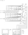
- FIG. 2 is a block diagram illustrating the circuit construction inside the casing 141 and eddy-current flaw detection device.
- the coils 111 to 118 in the first row are coils that are jointly used as magnetic field excitation coils and magnetic field detection coils, and each of these is connected to a multiplexer (switching circuit) 151 for magnetic field excitation, and to a multiplexer (switching circuit) 152 for magnetic field detection.
- a lead wire 159 is connected to the multiplexer 151 for magnetic field excitation, and an AC current for exciting a magnetic field is applied to the lead wire 159 from the main unit 164 of the eddy-current flaw detection device.
- An amplifier 156 which amplifies the output signal of the magnetic field that is detected by the coils 111 to 118, is connected to the multiplexer 152 for magnetic field detection, and the signal that is amplified by the amplifier 156 is outputted to the main unit 164 of the eddy-current flaw detection device via a lead wire 160.
- the coils 121 to 128 in the second row are also coils that are jointly used as magnetic field excitation coils and magnetic field detection coils, and each of these coils is connected to a multiplexer (switching circuit) 153 for magnetic field excitation, and to a multiplexer (switching circuit) 154 for magnetic field detection.
- a lead wire 161 is connected to the multiplexer 153 for magnetic field excitation, and an AC current for exciting a magnetic field is applied to the lead wire 161 from the main unit 164 of the eddy-current flaw detection device.
- An amplifier 157 which amplifies the output signal of the magnetic field that is detected by the coils 121 to 128, is connected to the multiplexer 154 for magnetic field detection, and the signal that is amplified by the amplifier 157 is outputted to the main unit 164 of the eddy-current flaw detection device via a lead wire 162.
- the coils 131 to 138 in the third row are magnetic field detection coils, and each of these is connected to a multiplexer (switching circuit) 155 for magnetic field detection.
- An amplifier 158 which amplifies the output signal of the magnetic field that is detected by the coils 131 to 138, is connected to the multiplexer 155 for magnetic field detection, and the signal that is amplified by the amplifier 158 is outputted to the main unit 164 of the eddy-current flaw detection device via a lead wire 163.
- the lead wires 159 to 163 are stored inside a cable 142 that connects the center section of the surface on one end of the casing 141 of the eddy-current flaw detection probe with the main unit 164 of the eddy-current flaw detection device.
- An oscillation circuit 165 that produces an AC current for exciting a magnetic field by coils 111 to 118 and 121 to 128, a signal detection circuit 166 that obtains amplified detection signals of magnetic fields that are detected by coils 111 to 118, 121 to 128 and 131 to 138, and a communication unit 167 for communicating with a personal computer (or workstation) 168 are stored inside of the main unit 164 of the eddy-current flaw detection device.
- the personal computer 168 receives the detection signal that was obtained by the signal detection circuit 166 via the communication unit 167 as detection data, and records and displays the received detection data.
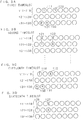
- FIGS. 3A to 3D are expanded views explaining the operation of an eddy-current flaw detection probe having this kind of construction, and illustrating a planar expansion of the coils 111 to 118, 121 to 128 and 131 to 138 shown in FIG. 1 .
- the multiplexer 151 selects coil 111 as the magnetic field excitation coil T, and multiplexer 152 selects coil 113, which is located at a position that differs two coils amount ahead of coil 111 in the circumferential direction of selection, as the magnetic field detection coil R.
- multiplexer 155 selects coils 131 and 132 in the third row, which are separated from coil 111 by an amount of 0.5 coil in the circumferential direction, as magnetic field detection coils R.
- the multiplexer 153 selects coil 121 in the second row, which is located at a position that differs 0.5 coil amount behind coil 111 in the circumferential direction of selection, as the magnetic field excitation coil T, and the multiplexer 154 selects coil 123, which is located at a position that differs two coils amount ahead of coil 121 in the circumferential direction of selection, as the magnetic field detection coil R.
- the multiplexer 151 sequentially selects coils 112, 113, 114, ... as the magnetic field excitation coil T, and the multiplexer 152 sequentially selects coils 114, 115, 116, ... as the magnetic field detection coil R.
- the multiplexer 155 sequentially selects two coils 132 ⁇ 133, 133 ⁇ 134, 134 ⁇ 135, ... as magnetic field detection coils R.
- the multiplexer 153 sequentially selects coils 122, 123, 124, ... as the magnetic field excitation coil T, and the multiplexer 154 sequentially selects coils 124, 125, 126 as the magnetic field detection coil R.
- the multiplexer 151 selects coil 118 as the magnetic field excitation coil T, and the multiplexer 152 selects coil 112, which is located at a position that differs two coils amount ahead of coil 118 in the circumferential direction of selection, as the magnetic field detection coil R.
- the multiplexer 155 selects coils 138, 131 in the third row, which are separated from coil 118 by an amount of 0.5 coil in the circumferential direction, as magnetic field detection coils R.
- the multiplexer 153 selects coil 128 in the second row, which is located at a position that differs 0.5 coil amount behind coil 118 in the circumferential direction of selection, as the magnetic field excitation coil T, and the multiplexer 154 selects coil 122, which is located at a position that differs two coils amount ahead of coil 128 in the circumferential direction of selection, as the magnetic field detection coil R.
- this flaw detection probe can obtain, for each circumference around a slim metal pipe, eight channels of output from coils 111 to 118 for detecting flaws in the circumferential direction, eight channels of output from coils 121 to 128 for detecting flaws in the circumferential direction, and 16 channels of output from coils 131 to coils 111 to 118 and the output signals from coils 121 to 128 are in a positional relationship that interpolate between each other in the circumferential direction, so the output for detecting flaws in the circumferential direction becomes a total of 16 channels.
- Japanese Patent Application Laid-Open No. 2000-235018 discloses an eddy-current flaw detection probe that comprises a plurality of excitation coils, a plurality of detection coils, and a switching circuit for time-division driving of these coils, and that further comprises an insulation switching circuit between the coils and switching circuit.
- Japanese Patent Application Laid-Open No. 2000-235019 discloses an eddy-current flaw detection probe that comprises a plurality of magnet field excitation elements, a plurality of magnetic field detection elements, a switching circuit for time-division driving of these elements, and a detection signal amplification circuit that is provided further on the measurement instrument side than the switching circuit that time-division drives the plurality of magnetic field detection elements.
- Japanese Patent Application Laid-Open No. 2000-235020 discloses an eddy-current flaw detection device that comprises an eddy-current flaw detection probe having a plurality of magnetic field excitation elements and magnetic field detection element pairs, and means for time-division driving of the magnetic field excitation elements and magnetic field detection element pairs of that probe, and further comprises a control device that includes means for keeping output signals from each element pair over a number of time-division driving steps, and means for finding the difference between the output signals from adjacent element pairs.
- US patent 5,506,503 relates to an eddy current probe for insertion into a tube to be inspected comprising a transmitter coil and a pair of sensing coils.
- EP 1 153 289 European patent application published as EP 1 153 289 relates to an eddy current testing probe.
- coils 111 to 118 and 121 to 128 are jointly used as magnetic field excitation coils and magnetic field detection coils, and are connected to both a switching circuit for magnetic field excitation and a switching circuit for magnetic field detection, so there are problems that circuit construction becomes complicated, and interference signals due to crosstalk occur.
- the present invention has been made with the aim of solving the above problems, and it is an object of the first aspect of the invention to provide an eddy-current flaw detection method that improves the spatial resolution of flaw detection signals and the signal reproducibility during redetection of flaws, and reduces signal interference due to crosstalk with a simple circuit construction.
- the object of further aspects of the invention is to provide an eddy-current flaw detection device that improves the spatial resolution of flaw detection signals and the signal reproducibility during redetection of flaws, and reduces signal interference due to crosstalk with a simple circuit construction.
- the object of further aspects of the invention is to provide an eddy-current flaw detection probe that improves the spatial resolution of flaw detection signals and the signal reproducibility during redetection of flaws, and reduces signal interference due to crosstalk with a simple circuit construction.
- the eddy-current flaw detection method involves performing eddy-current flaw detection of a conductive pipe by using: magnetic element groups of which magnetic elements, which either excite or detect a magnetic field, are evenly spaced in each of at least first and second rows that are formed, in the circumferential direction, around the surface of a column shaped casing that is formed such that it can be inserted into the conductive pipe, with the first row being located at a position that differs from the second row in which the magnetic elements detecting the magnetic field are placed by 1/2 the even spacing of the evenly spaced magnetic elements in the circumferential direction; a magnetic element group being located in a third row around the surface of the casing in the circumferential direction adjacent to the magnetic element group of the second row; and first, second and third switching circuits for selecting each magnetic element in the respective first, second and third rows of the magnetic element groups, characterized by comprising: a step of causing the first switching circuit to select in turn each magnetic element in the first row during corresponding time slots in order to excite
- an eddy-current flaw detection probe comprising: magnetic element groups of which magnetic elements, which either excite or detect a magnetic field, are evenly spaced in each of at least first and second rows that are formed, in the circumferential direction, around the surface of a column shaped casing that is formed such that it can be inserted into a conductive pipe, with the first row being located at a position that differs from the second row in which the magnetic elements detecting the magnetic field are placed by 1/2 the even spacing of the evenly spaced magnetic elements in the circumferential direction, a magnetic element group being located in a third row adjacent to the magnetic element group of the second row; and first, second and third switching circuits for selecting each magnetic element in the respective first, second and third rows of the magnetic element groups, characterized in that the magnetic elements in the first row are constructed as magnetic field excitation elements that excite a magnetic field by being selected in turn during corresponding time slots by the first switching circuit, the magnetic elements in the second row are constructed as magnetic field detection elements that detect a magnetic
- the eddy-current flaw detection method could include a step of preparing a magnetic element group that is located in a row around the surface of the casing adjacent to the other row, and a switching circuit for switching the magnetic element group at time-division; and a step of causing the switching circuit to switch, at time-division, two magnetic elements that are located in the row in order to detect the excited magnetic field.
- An example of an eddy current flaw detection device not covered by the invention is an eddy-current flaw detection device for performing eddy-current flaw detection of a conductive pipe, and comprising: a magnetic element group of which a specified number of magnetic elements are evenly spaced in each of at least two rows that are formed around the surface of a column shaped casing that is formed such that it can be inserted into the conductive pipe, with one of the two rows being located at a position that differs from the other row by 1/2 the even spacing in the row direction; and switching circuits for switching the magnetic elements in the respective row of the magnetic element group at time-division, and is characterized by comprising: magnetic field excitation means for causing the magnetic elements in one row to function as magnetic field excitation elements that excite magnetic fields by being switched at time-division by the switching circuit; and magnetic field detection means for causing the magnetic elements in the other row to function as magnetic field detection elements that detect magnetic fields by being switched at time-division by the switching circuit, wherein the eddy-
- a magnetic element group is provided of which a specified number of magnetic elements are evenly spaced in each of at least two rows that are formed around the surface of a column shaped casing that is formed such that it can be inserted into the conductive pipe, with one of the two rows being located at a position that differs from the other row by 1/2 the even spacing in the row direction, each switching circuit switches the magnetic elements in the respective row at time-division, and eddy-current flaw detection of the conductive pipe is performed.
- the magnetic elements in one row function as magnetic field excitation elements that excite magnetic fields by being switched at time-division
- magnetic elements in the other row function as magnetic field detection elements that detect magnetic fields by being switched at time-division.
- Eddy-current flaw detection of a conductive pipe is performed by detecting each magnetic field that is excited by each magnetic field excitation element by two of the magnetic field detection elements that are located at positions that differ from the magnetic field excitation element by 3/2 the even spacing in the row direction.
- the eddy-current flaw detection device is an eddy-current flaw detection device for performing eddy-current flaw detection of a conductive pipe, and comprising: a magnetic element group of which a specified number of magnetic elements are evenly spaced in each of at least two rows that are formed around the surface of a column shaped casing that is formed such that it can be inserted into the conductive pipe, with one of the two rows being located at a position that differs from the other row by 1/2 the even spacing in the row direction; and switching circuits for switching the magnetic elements in the respective row of the magnetic element group at time-division, and is characterized in that the magnetic elements in one row are magnetic field excitation elements that excite magnetic fields, the magnetic elements in the other row are magnetic field detection elements that detect magnetic fields, and eddy-current flaw detection of the conductive pipe is performed by detecting each magnetic field that is excited by each magnetic field excitation element being switched at time-division by the switching circuit by two magnetic field detection elements that are each located in the other row at positions that differ
- a magnetic element group is provided of which a specified number of magnetic elements are evenly spaced in each of at least two rows that are formed around the surface of a column shaped casing that is formed such that it can be inserted into the conductive pipe, with one of the two rows being located at a position that differs from the other row by 1/2 the even spacing in the row direction, each switching circuit switches the magnetic elements in the respective row at time-division, and eddy-current flaw detection of the conductive pipe is performed.
- the magnetic elements in one row are magnetic field excitation elements that excite a magnetic field
- the magnetic elements in the other row are magnetic detection elements that detect a magnetic field.
- Eddy-current flaw detection of the conductive pipe is performed by detecting each magnetic fields that are excited by each magnetic field excitation elements that are switched at time-division by two magnetic field detection elements that are each located in the other row at positions that differ from the magnetic field excitation element by 3/2 the even spacing in the row direction and that are switched at time-division.
- the eddy-current flaw detection device is an eddy-current flaw detection device comprising a magnetic element group of which a specified number of magnetic elements are evenly spaced in each of at least two rows, with one of the two rows being located at a position that differs from the other row by 1/2 the even spacing in the row direction, and switching circuits for switching the magnetic elements in the respective row of the magnetic element group at time-division; and is characterized by comprising: magnetic field excitation means for causing the magnetic elements in one row to function as magnetic field excitation elements that excite magnetic fields by being switched at time-division by the switching circuit, and magnetic field detection means for causing the magnetic elements in the other row to function as magnetic field detection elements that detect magnetic fields by being switched at time-division by the switching circuit, wherein the eddy-current flaw detection device performs eddy-current flaw detection by detecting each magnetic field that is excited by each magnetic field excitation element of the magnetic field excitation means by one or two magnetic field detection elements of the magnetic field detection means that are each
- a magnetic element group is provided of which a specified number of magnetic elements are evenly spaced in each of at least two rows, with one of the two rows being located at a position that differs from the other row by 1/2 the even spacing in the row direction, and each switching circuit switches the magnetic elements of each row at time-division.
- the magnetic elements in one row function as magnetic field excitation elements that excite a magnetic field by being switched at time-division
- the magnetic elements in the other row function as magnetic detection elements that detect a magnetic field by being switched at time-division.
- Eddy-current flaw detection is performed by detecting each magnetic field that is excited by each magnetic field excitation element by one or two magnetic field detection elements that are each located at positions that differ from the magnetic field excitation element by 3/2 the even spacing in the row direction.
- the eddy-current flaw detection device is an eddy-current flaw detection device comprising: a magnetic element group of which a specified number of magnetic elements are evenly spaced in each of at least two rows, with one of the two rows being located at a position that differs from the other row by 1/2 the even spacing in the row direction; and switching circuits for switching the magnetic elements in the respective row of the magnetic element group at time-division, and is characterized in that the magnetic elements in one row are magnetic field excitation elements that excite a magnetic field, the magnetic elements in the other row are magnetic field detection elements that detect a magnetic field, and eddy-current flaw detection is performed by detecting each magnetic field that is excited by each magnetic field excitation element that is switched at time-division by the switching circuit by one or two magnetic field detection elements that are each located in the other row at positions that differ from the magnetic field excitation element by 3/2 the even spacing in the row direction and that are switched at time-division by the switching circuit.
- a magnetic element group is provided of which a specified number of magnetic elements are evenly spaced in each of at least two rows, with one of the two rows being located at a position that differs from the other row by 1/2 the even spacing in the row direction, and each switching circuit switches the magnetic elements in the respective row at time-division.
- the magnetic elements in one row are magnetic field excitation elements that excite a magnetic field
- the magnetic elements in the other row are magnetic field detection elements that detect a magnetic field.
- Eddy-current flaw detection is performed by detecting each magnetic field that is excited by each magnetic field excitation element that is switched at time-division by one or two magnetic field detection elements that are each located in the other row at positions that differ from that of the magnetic field excitation element by 3/2 the even spacing in the row direction and that are switched at time-division.
- the eddy-current flaw detection device is characterized by further comprising a magnetic element group that is located in a row around the surface of the casing adjacent to the other row, and a switching circuit for switching the magnetic element group at time-division, and performing eddy-current flaw detection by detecting an excited magnetic field by two magnetic elements that are located in the row and that are switched by the switching circuit.
- another magnetic element group is additionally located in a row around the surface of the casing adjacent to the other row, and that additionally provided magnetic element group is switched at time-division by an additionally provided switching circuit.
- Eddy-current flaw detection is performed by detecting an excited magnetic field by two magnetic elements that are located in the additional row and that are switched at time-division bv the switching circuit.
- the eddy-current flaw detection device is characterized by further comprising an amplifier circuit for amplifying a signal that each of the magnetic field detection elements outputted via the switching circuit.
- the eddy-current flaw detection probe is an eddy-current flaw detection probe for performing eddy-current flaw detection of a conductive pipe, and comprising: a magnetic element group of which a specified number of elements are evenly spaced in each of at least two rows that are formed around the surface of a column shaped casing that is formed such that it can be inserted into the conductive pipe, with one of the two rows being located at a position that differs from that of the other row by 1/2 the even spacing in the row direction; and switching circuits for switching the magnetic elements in the respective row of the magnetic element group at time-division, and is characterized in that the magnetic elements in one row are constructed as magnetic field excitation elements that excite a magnetic field by being switched at time-division by the switching circuit, the magnetic elements in the other row are constructed as magnetic field detection elements that detect a magnetic field by being switched at time-division by the switching circuit, and eddy-current flaw detection of the conductive pipe is performed by detecting each magnetic field that is excited by each
- a magnetic element group is provided of which a specified number of elements are evenly spaced in each of at least two rows that are formed around the surface of a column shaped casing that is formed such that it can be inserted into a conductive pipe, with one of the two rows being located at a position that differs from that of the other row by 1/2 the even spacing in the row direction.
- Eddy-current flaw detection is performed by causing the switching circuits to switch the magnetic elements in the respective row at time-division.
- the magnetic elements in one row function as magnetic field excitation elements that excite a magnetic field by being switched at time-division
- the magnetic elements in the other row function as magnetic field detection elements that detect a magnetic field by being switched at time-division.
- Eddy-current flaw detection of a conductive pipe is performed by detecting each magnetic field that is excited by each magnetic element that functions as the magnetic field excitation element by two of the magnetic elements that function as magnetic field detection elements and that are located at positions that differ from that of the magnetic field excitation element by 3/2 the even spacing in the row direction.
- the eddy-current flaw detection probe is an eddy-current flaw detection probe for performing eddy-current flaw detection of a conductive pipe, and comprising: a magnetic element group of which a specified number of elements are evenly spaced in each of at least two rows that are formed around the surface of a column shaped casing that is formed such that it can be inserted into the conductive pipe, with one of the two rows being located at a position that differs from that of the other row by 1/2 the even spacing in the row direction; and switching circuits for switching the magnetic elements in the respective row of the magnetic element group at time-division, and is characterized in that the magnetic elements in one row are magnetic field excitation elements that excite a magnetic field, the magnetic elements in the other row are magnetic field detection elements that detect a magnetic field, and eddy-current flaw detection of the conductive pipe is performed by detecting each magnetic field that is excited by each magnetic field excitation element that is switched at time-division by the switching circuit by two magnetic field detection elements that are each located in the
- a magnetic element group is provided of which a specified number of magnetic elements are evenly spaced in each of at least two rows that are formed around the surface of a column shaped casing that is formed such that it can be inserted into a conductive pipe, with one of the two rows being located at a position that differs from that of the other row by 1/2 the even spacing in the row direction.
- Eddy-current flaw detection is performed by causing the switching circuits to switch the magnetic elements in the respective row at time-division.
- the magnetic elements in one row are magnetic field excitation elements that excite a magnetic field
- the magnetic elements in the other row are magnetic field detection elements that detect a magnetic field.
- Eddy-current flaw detection of the conductive pipe is performed by detecting each magnetic field that is excited by each magnetic field excitation element that is switched at time-division by two magnetic field detection elements that are each located in the other row at positions that differ from that of the magnetic field excitation element by 3/2 the even spacing in the row direction and that are switched at time-division.
- the eddy-current flaw detection probe is an eddy-current flaw detection probe that comprises: a magnetic element group of which a specified number of elements are evenly spaced in each of at least two rows, with one of the two rows being located at a position that differs from that of the other row by 1/2 the even spacing in the row direction; and switching circuits for switching the magnetic elements in the respective row of the magnetic element group at time-division, and is characterized in that the magnetic elements in one row are constructed as magnetic field excitation elements that excite a magnetic field by being switched at time-division by the switching circuit, the magnetic elements in the other row are constructed as magnetic field detection elements that detect a magnetic field by being switched at time-division by the switching circuit, and eddy-current flaw detection is performed by detecting each magnetic field that is excited by each magnetic element that functions as a magnetic field excitation element by one or two of the magnetic elements that function as the magnetic field detection elements and that are located at positions that differ from that of the magnetic field excitation element by 3/2 the even spacing in
- a magnetic element group is provided of which a specified number of magnetic elements are evenly spaced in each of at least two rows, with one of the two rows being located at a position that differs from that of the other row by 1/2 the even spacing in the row direction, and each switching circuit switches the magnetic elements in the respective row at time-division.
- the magnetic elements in one row function as magnetic field excitation elements that excite a magnetic field by being switched at time-division
- the magnetic elements in the other row function as magnetic field detection elements that detect a magnetic field by being switched at time-division.
- Eddy-current flaw detection is performed by detecting each magnetic field that is excited by each magnetic element that functions as the magnetic field excitation element by one or two of the magnetic elements that function as the magnetic field detection elements and that are located at positions that differ from that of the magnetic field excitation element by 3/2 the even spacing in the row direction.
- the eddy-current flaw detection probe is an eddy-current flaw detection probe that comprises: a magnetic element group of which a specified number of elements are evenly spaced in each of at least two rows, with one of the two rows being located at a position that differs from that of the other row by 1/2 the even spacing in the row direction; and switching circuits for switching the magnetic elements in the respective row of the magnetic element group at time-division, and is characterized in that the magnetic elements in one row are magnetic field excitation elements that excite a magnetic field, the magnetic elements in the other row are magnetic field detection elements that detect a magnetic field, and eddy-current flaw detection is performed by detecting each magnetic field that is excited by each magnetic field excitation element that is switched at time-division by the switching circuit by one or two magnetic field detection elements that are each located in the other row at positions that differ from the magnetic field excitation element by 3/2 the even spacing in the row direction and that are switched at time-division by the switching circuit.
- a magnetic element group is provided of which a specified number of magnetic elements are evenly spaced in each of at least two rows, with one of the two rows being located at a position that differs from that of the other row by 1/2 the even spacing in the row direction, each switching circuit switches the magnetic elements in the respective row at time-division.
- the magnetic elements in one row are magnetic field excitation elements that excite a magnetic field
- the magnetic elements in the other row are magnetic field detection elements that detect a magnetic field.
- Eddy-current flaw detection is performed by detecting each magnetic field that is excited by each magnetic field excitation element that is switched at time-division by one or two magnetic field detection elements that are each located in the other row at positions that differ from that of the magnetic field excitation element by 3/2 the even spacing in the row direction and that are switched at time-division.
- the eddy-current flaw detection probe is characterized by further comprising: a magnetic element group that is located in a row around the surface of the casing adjacent to the other row; and a switching circuit for switching the magnetic element group at time-division, and performing eddy-current flaw detection by detecting the excited magnetic field by two magnetic elements that are located in the row and that are switched at time-division.
- a magnetic element group is additionally provided in a row around the surface of the casing adjacent to the other row, and an additionally provided switching circuit switches the additionally provided magnetic element group at time-division.
- Eddy-current flaw detection is performed by detecting the excited magnetic field by switching two magnetic elements of that magnetic element group at time-division.
- the eddy-current flaw detection probe is characterized by further comprising an amplifier circuit for amplifying a signal that each of the magnetic field detection elements outputted via a switching circuit.
- the eddy-current flaw detection method it is possible to provide an eddy-current flaw detection method that improves the spatial resolution of flaw detection signals as well as signal reproducibility during redetection of flaws, and reduces signal interference due to crosstalk with a simple circuit construction.
- the eddy-current flaw detection device With the eddy-current flaw detection device according to the invention, it is possible to provide an eddy-current flaw detection device that improves the spatial resolution of flaw detection signals as well as signal reproducibility during redetection of flaws, and reduces signal interference due to crosstalk with a simple circuit construction.
- the eddy-current flaw detection probe With the eddy-current flaw detection probe according to the invention, it is possible to provide an eddy-current flaw detection probe that improves the spatial resolution of flaw detection signals as well as signal reproducibility during redetection of flaws, and reduces signal interference due to crosstalk with a simple circuit construction.
- FIG. 4 is a perspective drawing schematically illustrating the external appearance of an eddy-current flaw detection probe that is used in an embodiment of the eddy-current flaw detection method, eddy-current flaw detection device and eddy-current flaw detection probe of the present invention.
- This eddy-current flaw detection probe comprises a column shaped casing (housing) 41 that is formed such that it can be gently inserted inside a slim metal pipe, and eight coils 11 to 18, 21 to 28, 31 to 38, that are aligned around the outer surface of the casing 41, are evenly spaced in each of three rows.
- the coils 11 to 18 of the first row of the three rows are arranged such that they are located at a position in the circumferential direction that differs from that of the coils 21 to 28 and 31 to 38 of the other two rows by 1/2 the equal spacing.
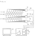
- FIG. 5 is a block diagram illustrating the circuit construction inside the casing 41 and eddy-current flaw detection device.
- the coils (magnetic elements, magnetic field excitation means) 11 to 18 in the first row are coils that are used as magnetic field excitation coils (magnetic field excitation elements) that generate an eddy current in the thickness section from the inner surface of a slim metal pipe, and each is connected to a multiplexer (switching circuit) 51 for magnetic field excitation.
- a lead wire 56 is connected to the multiplexer 51 for magnetic field excitation, and an AC current for exciting a magnetic field is applied to the lead wire 56 from the main unit 59 of the eddy-current flaw detection device.
- the coils (magnetic elements, magnetic field detection means) 21 to 28 in the second row are coils that are used as magnetic field detection coils (magnetic field detection elements) that detect a magnetic field according to an eddy current that is generated in the thickness section of a slim metal pipe, and each is connected to a multiplexer (switching circuit) 52 for magnetic field detection.
- An amplifier (magnetic field detection means) 54 which amplifies the output signals of the magnetic field that is detected by the coils 21 to 28, is connected to the multiplexer 52 for magnetic field detection, and the amplified signal from the amplifier 54 is outputted to the main unit 59 of the eddy-current flaw detection device via a lead wire 57.
- the coils (magnetic elements, magnetic field detection means) 31 to 38 in the third row are coils used for magnetic field detection, and each is connected to a multiplexer (switching circuit) 53 for magnetic field detection.
- An amplifier (magnetic field detection means) 55 which amplifies the output signal of the magnetic field that is detected by the coils 31 to 38, is connected to the multiplexer 53 for magnetic field detection, and the amplified signal from the amplifier 55 is outputted to the main unit 59 of the eddy-current flaw detection device via a lead wire 58.
- the lead wires 56 to 58 are stored inside a cable 42 that connects the center section of the surface on one end of the casing 41 of the eddy-current flaw detection probe with the main unit 59 of the eddy-current flaw detection device.
- An oscillation circuit (magnetic field excitation means) 60 that generates an AC current for exciting a magnetic field by the coils 11 to 18, a signal detection circuit 61 that obtains amplified detection signals of magnetic fields they are detected by coils 21 to 28 and 31 to 38, and a communication unit 62 for communicating with a personal computer (or workstation) 63 are located inside of the main unit 59 of the eddy-current flaw detection device.
- the personal computer 63 receives the detection signal that was obtained by the signal detection circuit 61 via the communication unit 62 as detection data, and records and displays the received detection data.
- the amplifiers 54 and 55 can also be located inside of the main unit 59 of the eddy-current flaw detection device, and when a small number of coils are in each row, the multiplexers 51 to 53 could also be located inside of the main unit 59 of the eddy-current flaw detection device.
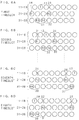
- FIGS. 6A to 6D are expanded views explaining the operation of an eddy-current flaw detection probe having this kind of construction, and illustrating a planar expansion of the coils 11 to 18, 21 to 28 and 31 to 38 shown in FIG. 4 .
- This eddy-current flaw detection probe detects flaws for the amount of one circumference of the inner surface of a slim metal pipe in first through eighth timeslots indicating the cycle of the operation.
- the multiplexer 51 selects coil 11 as the magnetic field excitation coil T, and the multiplexer 52 selects coils 28 and 23 in the second row, which are separated from the coil 11 by the amount of 3/2 coils in the circumferential direction, as magnetic field detection coils R1 and R2.
- the multiplexer 53 selects coils 31 and 32 in the third row, which are separated from coil 11 by the amount of 0.5 coil in the circumferential direction, as magnetic field detection coils R3 and R4.
- the detection signals that are outputted by the magnetic field detection coils R1, R2 are used for detecting flaws in the circumferential direction of the slim metal pipe (direction that orthogonally crosses the advancement direction of the eddy-current flaw detection probe), and the detection signals that are outputted by the magnetic field detection coils R3, R4 are used for detecting flaws in the axial direction of the slim metal pipe (advancement direction of the eddy-current flaw detection probe).
- the multiplexer 51 selects coil 12 as the magnetic field excitation coil T, and the multiplexer 52 selects coils 21 and 24 in the second row, which are separated from the coil 12 by the amount of 3/2 coils in the circumferential direction, as magnetic field detection coils R1 and R2.
- the multiplexer 53 selects coils 32 and 33 in the third row, which are separated from coil 12 by the amount of 0.5 coil in the circumferential direction, as magnetic field detection coils R3 and R4.
- the multiplexer 51 sequentially selects coils 13, 14, 15, ... as the magnetic field excitation coil T, and the multiplexer 52 sequentially selects pairs of coils 22 ⁇ 25, 23 ⁇ 26, 24 ⁇ 27, ...as the magnetic field detection coils R1 ⁇ R2.
- the multiplexer 53 sequentially selects pairs of coils 33 ⁇ 34, 34 ⁇ 35, 35 ⁇ 36, ... as the magnetic field detection coils R3 ⁇ R4.
- the multiplexer 51 selects coil 17 as the magnetic field excitation coil T, and the multiplexer 52 selects coils 26 and 21 in the second row, which are separated from the coil 17 by the amount of 3/2 coils in the circumferential direction, as magnetic field detection coils R1 and R2.
- the multiplexer 53 selects coils 37 and 38 in the third row, which are separated from coil 17 by the amount of 0.5 coil in the circumferential direction, as magnetic field detection coils R3 and R4.
- the multiplexer 51 selects coil 18 as the magnetic field excitation coil T, and the multiplexer 52 selects coils 27 and 22 in the second row, which are separated from the coil 18 by the amount of 3/2 coils in the circumferential direction, as magnetic field detection coils R1 and R2.
- the multiplexer 53 selects coils 38 and 31 in the third row, which are separated from coil 18 by the amount of 0.5 coil in the circumferential direction, as magnetic field detection coils R3 and R4.
- the combinations of the magnetic field excitation coil T and magnetic field detection coil R1, and the magnetic field excitation coil T and magnetic field detection coil R2 are suitably located for detecting flaws in the circumferential direction of the slim metal pipe (direction that orthogonally crosses the advancement direction of the eddy-current flaw detection probe). Also, the combinations of the magnetic field excitation coil T and the magnetic field detection coil R3, and the magnetic field excitation coil T and the magnetic field detection coil R4 are suitably located for detecting flaws in the axial direction of the slim metal pipe (advancement direction of the eddy-current flaw detection probe).
- FIG. 5 when compared with the conventional circuit shown in FIG. 2 , there is no need for two multiplexers, as well as there is no need for wiring from coils 11 to 18 of the first row and coils 21 to 28 of the second row to each of the two multiplexers, so the circuit construction can be made more compact, and the entire circuit can be stored inside the casing 41 of the eddy-current flaw detection probe. In addition, by reducing the amount of wiring, interference signals due to crosstalk can be reduced.
- the eddy-current flaw detection device it is possible to combine two timeslots. For example, in the first timeslot, it is possible to simultaneously select coils 11 and 15 as magnetic field excitation coils, and to simultaneously select coils 31, 32, 28, 23, 35, 36, 24 and 27 as magnetic field detection coils.
- An amplifier circuit is normally necessary in order to amplify detection signals from the multiplexer, however, in cases where the deterioration of the detection signals is not especially a problem, it is also possible to omit the amplifier circuit.
- this embodiment illustrates an example of an insert type probe that is inserted inside a slim metal pipe
- the present invention can also be applied to a top placement type or penetrating type eddy-current flaw detection device and eddy-current flaw detection probe.
- coils were used as both magnetic field excitation elements and magnetic field detection elements, however, the invention is not limited to this, and of course it is possible to use other elements. Also, a clear distinction is made between magnetic field excitation element groups and magnetic field detection element groups, so, for example, it is possible to combine different kinds of elements such using a coil as a magnetic field excitation element and using a magnetic detection element such as a hole element, magnetic resistance effect element and the like as a magnetic field detection element.
- the direction of the coils is not limited to that shown in FIG. 4 , and construction using other directions is possible.
- the number of coils is not necessarily limited to eight coils per row, and can be suitably increased or decreased as needed.
- the number of channels of the multiplexer which is a switching circuit, can be suitably increased or decreased as needed.
- the most preferable location for the circuit to be located is inside the casing of the eddy-current flaw detection probe, however, in the case where that is physically impossible, the circuit can be provided inside of or around the pipe that stores the wiring.
- the present invention can be applied to an eddy-current flaw detection method, eddy-current flaw detection device and eddy-current flaw detection probe that are used in nondestructive inspection (eddy-current flaw detection testing) of a heat transfer pipe inside of a heat exchanger.
Landscapes
- Chemical & Material Sciences (AREA)
- Chemical Kinetics & Catalysis (AREA)
- Electrochemistry (AREA)
- Physics & Mathematics (AREA)
- Health & Medical Sciences (AREA)
- Life Sciences & Earth Sciences (AREA)
- Analytical Chemistry (AREA)
- Biochemistry (AREA)
- General Health & Medical Sciences (AREA)
- General Physics & Mathematics (AREA)
- Immunology (AREA)
- Pathology (AREA)
- Investigating Or Analyzing Materials By The Use Of Magnetic Means (AREA)
Claims (4)
- Procédé de détection de défauts par courants de Foucault pour réaliser une détection de défauts par courants de Foucault d'un tuyau conducteur en utilisant : des groupes d'éléments magnétiques dont des éléments magnétiques (11 à 18, 21 à 28), qui soit excitent soit détectent un champ magnétique, sont espacés régulièrement dans chacune d'une première et d'une deuxième rangée qui sont formées, dans la direction circonférentielle, autour de la surface d'un boîtier en forme de colonne (41), un groupe d'éléments magnétiques (31 à 38) étant situé dans une troisième rangée autour de la surface du boîtier (41) dans la direction circonférentielle et adjacent au groupe d'éléments magnétiques (21 à 28) de la deuxième rangée, le boîtier en forme de colonne (41) étant formé de telle sorte qu'il puisse être inséré dans le tuyau conducteur, avec la première rangée située à une position qui diffère par rapport à chacune des deuxième et troisième rangées dans laquelle les éléments magnétiques détectant le champ magnétique sont placés à 1/2 de l'espacement régulier des éléments magnétiques espacés régulièrement dans la direction circonférentielle ; et des premier, deuxième et troisième circuits de commutation (51, 52, 53) pour sélectionner chaque élément magnétique (11 à 18, 21 à 28, 31 à 38) dans les première, deuxième et troisième rangées respectives des groupes d'éléments magnétiques, caractérisé en ce qu'il comprend :une étape consistant à amener le premier circuit de commutation (51) à sélectionner tour à tour chaque élément magnétique (11 à 18) se trouvant dans la première rangée pendant des créneaux temporels correspondants afin d'exciter un champ magnétique ;une étape consistant à amener le deuxième circuit de commutation (52) à sélectionner, pendant des créneaux temporels correspondants, des éléments magnétiques (21 à 28) de la deuxième rangée deux à la fois de manière séquentielle, chaque groupe de deux éléments magnétiques sélectionnés de la deuxième rangée étant situé à des positions qui diffèrent par rapport à l'élément magnétique (11 à 18) qui a excité le champ magnétique de 3/2 de l'espacement régulier des éléments magnétiques espacés régulièrement dans la direction circonférentielle afin de détecter le champ magnétique excité ; etune étape consistant à amener le troisième circuit de commutation (53) à sélectionner, pendant des créneaux temporels correspondants, des éléments magnétiques (31 à 38) de la troisième rangée deux à la fois de manière séquentielle, chaque groupe de deux éléments magnétiques sélectionnés de la troisième rangée étant situé à des positions qui diffèrent par rapport à l'élément magnétique (11 à 18) qui a excité le champ magnétique de 1/2 de l'espacement régulier des éléments magnétiques espacés régulièrement dans la direction circonférentielle afin de détecter le champ magnétique excité.
- Sonde de détection de défauts par courants de Foucault, comprenant : des groupes d'éléments magnétiques dont des éléments magnétiques (11 à 18, 21 à 28), qui soit excitent soit détectent un champ magnétique, sont espacés régulièrement dans chacune d'une première et d'une deuxième rangée qui sont formées, dans la direction circonférentielle, autour de la surface d'un boîtier en forme de colonne (41), un groupe d'éléments magnétiques (31 à 38) étant situé dans une troisième rangée autour de la surface du boîtier (41) dans la direction circonférentielle et adjacent au groupe d'éléments magnétiques (21 à 28) de la deuxième rangée, le boîtier en forme de colonne étant formé de telle sorte qu'il puisse être inséré dans le tuyau conducteur, avec la première rangée située à une position qui diffère par rapport à chacune des deuxième et troisième rangées dans laquelle les éléments magnétiques détectant le champ magnétique sont placés à 1/2 de l'espacement régulier des éléments magnétiques espacés régulièrement dans la direction circonférentielle ; et des premier, deuxième et troisième circuits de commutation (51, 52, 53) pour sélectionner chaque élément magnétique (11 à 18, 21 à 28, 31 à 38) dans les première, deuxième et troisième rangées respectives des groupes d'éléments magnétiques, caractérisé en ce que :le premier circuit de commutation (51) est adapté à sélectionner tour à tour pendant des créneaux temporels correspondants les éléments magnétiques (11 à 18) se trouvant dans la première rangée pour exciter un champ magnétique,le deuxième circuit de commutation (52) est adapté à sélectionner tour à tour pendant des créneaux temporels correspondants, les éléments magnétiques (21 à 28) se trouvant dans la deuxième rangée pour détecter un champ magnétique ; etla sonde de détection de défauts par courants de Foucault étant adaptée à exécuter une détection de défauts par courants de Foucault en détectant chaque champ magnétique qui est excité par chaque élément magnétique (11 à 18) qui fonctionne comme élément d'excitation de champ magnétique en sélectionnant par le deuxième circuit de commutation (53) des éléments magnétiques (21 à 28) de la deuxième rangée deux à la fois de manière séquentielle pendant des créneaux temporels correspondants, chaque groupe de deux éléments magnétiques sélectionnés de la deuxième rangée fonctionnant comme éléments de détection de champ magnétique et étant situé à des positions qui diffèrent par rapport à l'élément d'excitation de magnétique (11 à 18) de 3/2 de l'espacement régulier des éléments magnétiques espacés régulièrement dans la direction circonférentielle et en détectant le champ magnétique excité en sélectionnant par le troisième circuit de commutation (53) des éléments magnétiques (31 à 38) de la troisième rangée deux à la fois de manière séquentielle pendant des créneaux temporels correspondants, chaque groupe de deux éléments magnétiques sélectionnés de la troisième rangée étant situé à des positions qui diffèrent par rapport à l'élément d'excitation de champ magnétique (11 à 18) de 1/2 de l'espacement régulier des éléments magnétiques espacés régulièrement dans la direction circonférentielle.
- Sonde de détection de défauts par courants de Foucault selon la revendication 2, comprenant en outre un circuit amplificateur (54, 55) pour amplifier un signal que chacun des éléments de détection de champ magnétique (21 à 28, 31 à 38) a produit en sortie par l'intermédiaire du circuit de commutation (52, 53).
- Dispositif de détection de défauts par courants de Foucault, comprenant :la sonde de la revendication 2 ou 3 ;des moyens d'excitation de champ magnétique (60) pour amener les éléments magnétiques (11 à 18) se trouvant dans la première rangée à fonctionner comme des éléments d'excitation de champ magnétique qui excitent un champ magnétique en étant sélectionnés tour à tour pendant des créneaux temporels correspondants par le circuit de commutation (51) ; etdes moyens de détection de champ magnétique (61) pour amener les éléments magnétiques (21 à 28) se trouvant dans la deuxième rangée à fonctionner comme des éléments de détection de champ magnétique qui détectent un champ magnétique en étant sélectionnés pendant des créneaux temporels correspondants par le circuit de commutation (52).
Applications Claiming Priority (2)
| Application Number | Priority Date | Filing Date | Title |
|---|---|---|---|
| JP2007244461A JP5175513B2 (ja) | 2007-09-20 | 2007-09-20 | 渦流探傷方法、渦流探傷装置及び渦流探傷プローブ |
| PCT/JP2008/065504 WO2009037954A1 (fr) | 2007-09-20 | 2008-08-29 | Procédé de détection de défauts par courants de foucault, dispositif de détection de défauts par courants de foucault et sonde de détection de défauts par courants de foucault |
Publications (3)
| Publication Number | Publication Date |
|---|---|
| EP2199785A1 EP2199785A1 (fr) | 2010-06-23 |
| EP2199785A4 EP2199785A4 (fr) | 2014-04-23 |
| EP2199785B1 true EP2199785B1 (fr) | 2020-01-22 |
Family
ID=40467774
Family Applications (1)
| Application Number | Title | Priority Date | Filing Date |
|---|---|---|---|
| EP08831388.7A Active EP2199785B1 (fr) | 2007-09-20 | 2008-08-29 | Procédé de détection de défauts par courants de foucault, dispositif de détection de défauts par courants de foucault et sonde de détection de défauts par courants de foucault |
Country Status (8)
| Country | Link |
|---|---|
| US (1) | US8421449B2 (fr) |
| EP (1) | EP2199785B1 (fr) |
| JP (1) | JP5175513B2 (fr) |
| KR (1) | KR101450842B1 (fr) |
| CN (1) | CN101802603B (fr) |
| CA (1) | CA2700208C (fr) |
| ES (1) | ES2779531T3 (fr) |
| WO (1) | WO2009037954A1 (fr) |
Families Citing this family (25)
| Publication number | Priority date | Publication date | Assignee | Title |
|---|---|---|---|---|
| CA2771291A1 (fr) * | 2009-08-14 | 2011-02-17 | Paul Lott | Appareil et procede d'inspection de conduite |
| FR2965356A1 (fr) * | 2010-09-23 | 2012-03-30 | Airbus Operations Sas | Controle non destructif d'une structure dans un aeronef |
| FR2974416B1 (fr) * | 2011-04-21 | 2014-08-22 | Eads Europ Aeronautic Defence | Dispositif d'inspection non destructive d'une lumiere et procede d'inspection associe |
| US20130214771A1 (en) * | 2012-01-25 | 2013-08-22 | Radiation Monitoring Devices, Inc. | Systems and methods for inspecting structures including pipes and reinforced concrete |
| JP6062158B2 (ja) * | 2012-05-18 | 2017-01-18 | 株式会社東芝 | 渦電流探傷装置および方法 |
| JP5959306B2 (ja) * | 2012-05-21 | 2016-08-02 | 株式会社東芝 | 渦電流探傷装置及び方法 |
| US20150177191A1 (en) * | 2012-06-21 | 2015-06-25 | Eddyfi Ndt Inc. | High resolution eddy current array probe |
| JP5922633B2 (ja) | 2013-10-22 | 2016-05-24 | 三菱重工業株式会社 | 渦電流探傷プローブ、及び、渦電流探傷方法 |
| US20150338377A1 (en) * | 2014-05-20 | 2015-11-26 | Zetec, Inc. | Eddy Current Inspection Probe |
| CN105806929A (zh) * | 2014-12-30 | 2016-07-27 | 中核武汉核电运行技术股份有限公司 | 一种铁磁性薄壁管周向交流磁化漏磁检测的阵列探头 |
| CN104698076A (zh) * | 2015-02-06 | 2015-06-10 | 成都思驰科技有限公司 | 一种基于电涡流效应的金属管道多点在线探伤装置及方法 |
| CN104792861B (zh) * | 2015-05-20 | 2018-05-29 | 上海海事大学 | 一种检测导电结构缺陷的柔性阵列涡流探头及检测方法 |
| JP6472334B2 (ja) * | 2015-06-03 | 2019-02-20 | 日立Geニュークリア・エナジー株式会社 | 渦電流検査装置 |
| CN105004786B (zh) * | 2015-08-17 | 2017-10-31 | 苏州热工研究院有限公司 | 一种基于涡流检测的换热管管壁凹陷程度评估方法 |
| JP6621336B2 (ja) * | 2016-02-02 | 2019-12-18 | 日立Geニュークリア・エナジー株式会社 | 検査装置 |
| JP6751645B2 (ja) * | 2016-10-20 | 2020-09-09 | 日立Geニュークリア・エナジー株式会社 | 渦電流探傷システム及び渦電流探傷方法 |
| KR101941354B1 (ko) * | 2017-01-03 | 2019-01-22 | 한국수력원자력 주식회사 | 송수신부가 절연된 배열 와전류 탐촉자 및 이를 이용한 와전류 탐상 검사 방법 |
| CN106959337A (zh) * | 2017-05-03 | 2017-07-18 | 河南科技大学 | 一种开放式微磁激励钢丝绳损伤检测系统 |
| JP6879969B2 (ja) * | 2018-03-19 | 2021-06-02 | 三菱重工業株式会社 | 渦電流探傷プローブ |
| JP7231357B2 (ja) * | 2018-08-30 | 2023-03-01 | 矢崎エナジーシステム株式会社 | 導体劣化検出装置 |
| CN109521088B (zh) * | 2018-12-28 | 2023-09-29 | 中国石油大学(华东) | 一种检测管道缺陷的多通道脉冲涡流检测装置及方法 |
| US11499940B2 (en) | 2019-01-22 | 2022-11-15 | Zetec, Inc. | Eddy current probe |
| JP7227794B2 (ja) * | 2019-03-01 | 2023-02-22 | 三菱重工業株式会社 | 渦電流探傷プローブ、探傷方法 |
| CN111044607B (zh) * | 2019-12-26 | 2023-06-30 | 爱德森(厦门)电子有限公司 | 一种改进型正交电扰动涡流传感器 |
| KR102265354B1 (ko) * | 2019-12-30 | 2021-06-14 | 조선대학교산학협력단 | 자기렌즈를 구비한 환형 배열 와전류프로브 비파괴검사 장치 |
Family Cites Families (13)
| Publication number | Priority date | Publication date | Assignee | Title |
|---|---|---|---|---|
| CA2076205C (fr) * | 1992-08-14 | 1999-04-20 | Valentino S. Cecco | Sonde a courant de foucault differentiel a bracelets a bobinages multiples |
| JPH08334498A (ja) * | 1995-06-08 | 1996-12-17 | Ishikawajima Harima Heavy Ind Co Ltd | 全方位渦流探傷方法およびその装置 |
| JP3276295B2 (ja) * | 1996-10-09 | 2002-04-22 | 三菱重工業株式会社 | 渦電流探傷装置 |
| FR2758393B1 (fr) * | 1997-01-10 | 1999-10-15 | Commissariat Energie Atomique | Sonde a courants de foucault |
| JP2000235018A (ja) | 1999-02-12 | 2000-08-29 | Genshiryoku Engineering:Kk | 渦流探傷プローブ |
| US6344739B1 (en) * | 1999-02-12 | 2002-02-05 | R/D Tech Inc. | Eddy current probe with multi-use coils and compact configuration |
| JP2000235020A (ja) | 1999-02-12 | 2000-08-29 | Genshiryoku Engineering:Kk | 渦流探傷装置 |
| JP2000235019A (ja) * | 1999-02-12 | 2000-08-29 | Genshiryoku Engineering:Kk | 渦流探傷プローブ |
| AU2530100A (en) * | 1999-02-12 | 2000-08-29 | R.D. Tech | Multi-element probe with multiplexed elements for non-destructive testing |
| US6888346B2 (en) * | 2000-11-28 | 2005-05-03 | The United States Of America As Represented By The Administrator Of The National Aeronautics And Space Administration | Magnetoresistive flux focusing eddy current flaw detection |
| JP2003344360A (ja) * | 2002-05-23 | 2003-12-03 | Central Res Inst Of Electric Power Ind | 3次元形状物検査装置 |
| JP4561195B2 (ja) * | 2004-06-24 | 2010-10-13 | Jfeスチール株式会社 | 磁性金属被検体の欠陥の検出方法及びその検出装置 |
| JP4327745B2 (ja) * | 2005-02-18 | 2009-09-09 | 株式会社日立製作所 | 渦電流探傷プローブ及び渦電流探傷装置 |
-
2007
- 2007-09-20 JP JP2007244461A patent/JP5175513B2/ja active Active
-
2008
- 2008-08-29 CN CN2008801078792A patent/CN101802603B/zh not_active Expired - Fee Related
- 2008-08-29 US US12/679,222 patent/US8421449B2/en active Active
- 2008-08-29 ES ES08831388T patent/ES2779531T3/es active Active
- 2008-08-29 KR KR1020107007293A patent/KR101450842B1/ko not_active Expired - Fee Related
- 2008-08-29 CA CA2700208A patent/CA2700208C/fr active Active
- 2008-08-29 WO PCT/JP2008/065504 patent/WO2009037954A1/fr not_active Ceased
- 2008-08-29 EP EP08831388.7A patent/EP2199785B1/fr active Active
Non-Patent Citations (1)
| Title |
|---|
| None * |
Also Published As
| Publication number | Publication date |
|---|---|
| ES2779531T3 (es) | 2020-08-18 |
| CA2700208C (fr) | 2017-12-12 |
| US8421449B2 (en) | 2013-04-16 |
| JP5175513B2 (ja) | 2013-04-03 |
| CA2700208A1 (fr) | 2009-03-26 |
| KR20100080528A (ko) | 2010-07-08 |
| CN101802603A (zh) | 2010-08-11 |
| KR101450842B1 (ko) | 2014-10-14 |
| WO2009037954A1 (fr) | 2009-03-26 |
| CN101802603B (zh) | 2012-07-25 |
| EP2199785A1 (fr) | 2010-06-23 |
| US20100231210A1 (en) | 2010-09-16 |
| EP2199785A4 (fr) | 2014-04-23 |
| JP2009074943A (ja) | 2009-04-09 |
Similar Documents
| Publication | Publication Date | Title |
|---|---|---|
| EP2199785B1 (fr) | Procédé de détection de défauts par courants de foucault, dispositif de détection de défauts par courants de foucault et sonde de détection de défauts par courants de foucault | |
| JP5390383B2 (ja) | 導電部に対する渦電流試験を行うための放出/受信機能を別々に備えた装置 | |
| EP1153289B1 (fr) | Essai par courant de foucault a l'aide d'une configuration compacte | |
| CA2842888C (fr) | Sonde a groupement a courant de foucault a haute resolution | |
| JP4917899B2 (ja) | 渦電流探傷センサ及び渦電流探傷方法 | |
| US8344725B2 (en) | Device for nondestructive testing of pipes | |
| US7948233B2 (en) | Omnidirectional eddy current array probes and methods of use | |
| KR101941354B1 (ko) | 송수신부가 절연된 배열 와전류 탐촉자 및 이를 이용한 와전류 탐상 검사 방법 | |
| EP2866027B1 (fr) | Capteur de courant de Foucault avec conducteur de mécanisme d'induction linéaire | |
| JP2000235019A (ja) | 渦流探傷プローブ | |
| CA3089556A1 (fr) | Sonde pour essais non destructifs par courants de foucault | |
| JP4118488B2 (ja) | 離隔渦流法による管の肉厚測定装置 | |
| JP2001509259A (ja) | 渦流検査装置 | |
| CN116465958A (zh) | 一种阵列式可伸缩探头、脉冲涡流无损探伤系统及方法 | |
| JP2000235018A (ja) | 渦流探傷プローブ | |
| JP2010032352A (ja) | 渦流探傷方法及び装置 | |
| JP2023028986A (ja) | プローブ、プローブ装置、プローブシステム及び渦電流探傷方法 |
Legal Events
| Date | Code | Title | Description |
|---|---|---|---|
| PUAI | Public reference made under article 153(3) epc to a published international application that has entered the european phase |
Free format text: ORIGINAL CODE: 0009012 |
|
| 17P | Request for examination filed |
Effective date: 20100420 |
|
| AK | Designated contracting states |
Kind code of ref document: A1 Designated state(s): AT BE BG CH CY CZ DE DK EE ES FI FR GB GR HR HU IE IS IT LI LT LU LV MC MT NL NO PL PT RO SE SI SK TR |
|
| AX | Request for extension of the european patent |
Extension state: AL BA MK RS |
|
| DAX | Request for extension of the european patent (deleted) | ||
| A4 | Supplementary search report drawn up and despatched |
Effective date: 20140325 |
|
| RIC1 | Information provided on ipc code assigned before grant |
Ipc: G01N 27/90 20060101AFI20140319BHEP |
|
| STAA | Information on the status of an ep patent application or granted ep patent |
Free format text: STATUS: EXAMINATION IS IN PROGRESS |
|
| 17Q | First examination report despatched |
Effective date: 20170510 |
|
| GRAP | Despatch of communication of intention to grant a patent |
Free format text: ORIGINAL CODE: EPIDOSNIGR1 |
|
| STAA | Information on the status of an ep patent application or granted ep patent |
Free format text: STATUS: GRANT OF PATENT IS INTENDED |
|
| INTG | Intention to grant announced |
Effective date: 20190830 |
|
| GRAS | Grant fee paid |
Free format text: ORIGINAL CODE: EPIDOSNIGR3 |
|
| GRAA | (expected) grant |
Free format text: ORIGINAL CODE: 0009210 |
|
| STAA | Information on the status of an ep patent application or granted ep patent |
Free format text: STATUS: THE PATENT HAS BEEN GRANTED |
|
| AK | Designated contracting states |
Kind code of ref document: B1 Designated state(s): AT BE BG CH CY CZ DE DK EE ES FI FR GB GR HR HU IE IS IT LI LT LU LV MC MT NL NO PL PT RO SE SI SK TR |
|
| REG | Reference to a national code |
Ref country code: GB Ref legal event code: FG4D |
|
| REG | Reference to a national code |
Ref country code: CH Ref legal event code: EP |
|
| REG | Reference to a national code |
Ref country code: AT Ref legal event code: REF Ref document number: 1227224 Country of ref document: AT Kind code of ref document: T Effective date: 20200215 |
|
| REG | Reference to a national code |
Ref country code: IE Ref legal event code: FG4D |
|
| REG | Reference to a national code |
Ref country code: DE Ref legal event code: R096 Ref document number: 602008062046 Country of ref document: DE |
|
| REG | Reference to a national code |
Ref country code: NL Ref legal event code: MP Effective date: 20200122 |
|
| REG | Reference to a national code |
Ref country code: LT Ref legal event code: MG4D |
|
| PG25 | Lapsed in a contracting state [announced via postgrant information from national office to epo] |
Ref country code: PT Free format text: LAPSE BECAUSE OF FAILURE TO SUBMIT A TRANSLATION OF THE DESCRIPTION OR TO PAY THE FEE WITHIN THE PRESCRIBED TIME-LIMIT Effective date: 20200614 Ref country code: NL Free format text: LAPSE BECAUSE OF FAILURE TO SUBMIT A TRANSLATION OF THE DESCRIPTION OR TO PAY THE FEE WITHIN THE PRESCRIBED TIME-LIMIT Effective date: 20200122 Ref country code: NO Free format text: LAPSE BECAUSE OF FAILURE TO SUBMIT A TRANSLATION OF THE DESCRIPTION OR TO PAY THE FEE WITHIN THE PRESCRIBED TIME-LIMIT Effective date: 20200422 Ref country code: FI Free format text: LAPSE BECAUSE OF FAILURE TO SUBMIT A TRANSLATION OF THE DESCRIPTION OR TO PAY THE FEE WITHIN THE PRESCRIBED TIME-LIMIT Effective date: 20200122 |
|
| REG | Reference to a national code |
Ref country code: ES Ref legal event code: FG2A Ref document number: 2779531 Country of ref document: ES Kind code of ref document: T3 Effective date: 20200818 |
|
| PG25 | Lapsed in a contracting state [announced via postgrant information from national office to epo] |
Ref country code: IS Free format text: LAPSE BECAUSE OF FAILURE TO SUBMIT A TRANSLATION OF THE DESCRIPTION OR TO PAY THE FEE WITHIN THE PRESCRIBED TIME-LIMIT Effective date: 20200522 Ref country code: GR Free format text: LAPSE BECAUSE OF FAILURE TO SUBMIT A TRANSLATION OF THE DESCRIPTION OR TO PAY THE FEE WITHIN THE PRESCRIBED TIME-LIMIT Effective date: 20200423 Ref country code: HR Free format text: LAPSE BECAUSE OF FAILURE TO SUBMIT A TRANSLATION OF THE DESCRIPTION OR TO PAY THE FEE WITHIN THE PRESCRIBED TIME-LIMIT Effective date: 20200122 Ref country code: SE Free format text: LAPSE BECAUSE OF FAILURE TO SUBMIT A TRANSLATION OF THE DESCRIPTION OR TO PAY THE FEE WITHIN THE PRESCRIBED TIME-LIMIT Effective date: 20200122 Ref country code: LV Free format text: LAPSE BECAUSE OF FAILURE TO SUBMIT A TRANSLATION OF THE DESCRIPTION OR TO PAY THE FEE WITHIN THE PRESCRIBED TIME-LIMIT Effective date: 20200122 Ref country code: BG Free format text: LAPSE BECAUSE OF FAILURE TO SUBMIT A TRANSLATION OF THE DESCRIPTION OR TO PAY THE FEE WITHIN THE PRESCRIBED TIME-LIMIT Effective date: 20200422 |
|
| REG | Reference to a national code |
Ref country code: DE Ref legal event code: R097 Ref document number: 602008062046 Country of ref document: DE |
|
| PG25 | Lapsed in a contracting state [announced via postgrant information from national office to epo] |
Ref country code: DK Free format text: LAPSE BECAUSE OF FAILURE TO SUBMIT A TRANSLATION OF THE DESCRIPTION OR TO PAY THE FEE WITHIN THE PRESCRIBED TIME-LIMIT Effective date: 20200122 Ref country code: EE Free format text: LAPSE BECAUSE OF FAILURE TO SUBMIT A TRANSLATION OF THE DESCRIPTION OR TO PAY THE FEE WITHIN THE PRESCRIBED TIME-LIMIT Effective date: 20200122 Ref country code: LT Free format text: LAPSE BECAUSE OF FAILURE TO SUBMIT A TRANSLATION OF THE DESCRIPTION OR TO PAY THE FEE WITHIN THE PRESCRIBED TIME-LIMIT Effective date: 20200122 Ref country code: RO Free format text: LAPSE BECAUSE OF FAILURE TO SUBMIT A TRANSLATION OF THE DESCRIPTION OR TO PAY THE FEE WITHIN THE PRESCRIBED TIME-LIMIT Effective date: 20200122 Ref country code: CZ Free format text: LAPSE BECAUSE OF FAILURE TO SUBMIT A TRANSLATION OF THE DESCRIPTION OR TO PAY THE FEE WITHIN THE PRESCRIBED TIME-LIMIT Effective date: 20200122 Ref country code: SK Free format text: LAPSE BECAUSE OF FAILURE TO SUBMIT A TRANSLATION OF THE DESCRIPTION OR TO PAY THE FEE WITHIN THE PRESCRIBED TIME-LIMIT Effective date: 20200122 |
|
| REG | Reference to a national code |
Ref country code: AT Ref legal event code: MK05 Ref document number: 1227224 Country of ref document: AT Kind code of ref document: T Effective date: 20200122 |
|
| PLBE | No opposition filed within time limit |
Free format text: ORIGINAL CODE: 0009261 |
|
| STAA | Information on the status of an ep patent application or granted ep patent |
Free format text: STATUS: NO OPPOSITION FILED WITHIN TIME LIMIT |
|
| 26N | No opposition filed |
Effective date: 20201023 |
|
| PG25 | Lapsed in a contracting state [announced via postgrant information from national office to epo] |
Ref country code: IT Free format text: LAPSE BECAUSE OF FAILURE TO SUBMIT A TRANSLATION OF THE DESCRIPTION OR TO PAY THE FEE WITHIN THE PRESCRIBED TIME-LIMIT Effective date: 20200122 Ref country code: AT Free format text: LAPSE BECAUSE OF FAILURE TO SUBMIT A TRANSLATION OF THE DESCRIPTION OR TO PAY THE FEE WITHIN THE PRESCRIBED TIME-LIMIT Effective date: 20200122 |
|
| PG25 | Lapsed in a contracting state [announced via postgrant information from national office to epo] |
Ref country code: PL Free format text: LAPSE BECAUSE OF FAILURE TO SUBMIT A TRANSLATION OF THE DESCRIPTION OR TO PAY THE FEE WITHIN THE PRESCRIBED TIME-LIMIT Effective date: 20200122 Ref country code: SI Free format text: LAPSE BECAUSE OF FAILURE TO SUBMIT A TRANSLATION OF THE DESCRIPTION OR TO PAY THE FEE WITHIN THE PRESCRIBED TIME-LIMIT Effective date: 20200122 |
|
| REG | Reference to a national code |
Ref country code: DE Ref legal event code: R119 Ref document number: 602008062046 Country of ref document: DE |
|
| PG25 | Lapsed in a contracting state [announced via postgrant information from national office to epo] |
Ref country code: MC Free format text: LAPSE BECAUSE OF FAILURE TO SUBMIT A TRANSLATION OF THE DESCRIPTION OR TO PAY THE FEE WITHIN THE PRESCRIBED TIME-LIMIT Effective date: 20200122 |
|
| REG | Reference to a national code |
Ref country code: CH Ref legal event code: PL |
|
| GBPC | Gb: european patent ceased through non-payment of renewal fee |
Effective date: 20200829 |
|
| PG25 | Lapsed in a contracting state [announced via postgrant information from national office to epo] |
Ref country code: LI Free format text: LAPSE BECAUSE OF NON-PAYMENT OF DUE FEES Effective date: 20200831 Ref country code: CH Free format text: LAPSE BECAUSE OF NON-PAYMENT OF DUE FEES Effective date: 20200831 Ref country code: LU Free format text: LAPSE BECAUSE OF NON-PAYMENT OF DUE FEES Effective date: 20200829 |
|
| REG | Reference to a national code |
Ref country code: BE Ref legal event code: MM Effective date: 20200831 |
|
| PG25 | Lapsed in a contracting state [announced via postgrant information from national office to epo] |
Ref country code: DE Free format text: LAPSE BECAUSE OF NON-PAYMENT OF DUE FEES Effective date: 20210302 |
|
| PG25 | Lapsed in a contracting state [announced via postgrant information from national office to epo] |
Ref country code: BE Free format text: LAPSE BECAUSE OF NON-PAYMENT OF DUE FEES Effective date: 20200831 Ref country code: IE Free format text: LAPSE BECAUSE OF NON-PAYMENT OF DUE FEES Effective date: 20200829 Ref country code: GB Free format text: LAPSE BECAUSE OF NON-PAYMENT OF DUE FEES Effective date: 20200829 |
|
| PG25 | Lapsed in a contracting state [announced via postgrant information from national office to epo] |
Ref country code: TR Free format text: LAPSE BECAUSE OF FAILURE TO SUBMIT A TRANSLATION OF THE DESCRIPTION OR TO PAY THE FEE WITHIN THE PRESCRIBED TIME-LIMIT Effective date: 20200122 Ref country code: MT Free format text: LAPSE BECAUSE OF FAILURE TO SUBMIT A TRANSLATION OF THE DESCRIPTION OR TO PAY THE FEE WITHIN THE PRESCRIBED TIME-LIMIT Effective date: 20200122 Ref country code: CY Free format text: LAPSE BECAUSE OF FAILURE TO SUBMIT A TRANSLATION OF THE DESCRIPTION OR TO PAY THE FEE WITHIN THE PRESCRIBED TIME-LIMIT Effective date: 20200122 |
|
| PGFP | Annual fee paid to national office [announced via postgrant information from national office to epo] |
Ref country code: ES Payment date: 20250908 Year of fee payment: 18 |
|
| PGFP | Annual fee paid to national office [announced via postgrant information from national office to epo] |
Ref country code: FR Payment date: 20250827 Year of fee payment: 18 |